EP0701257A2 - Equilibration rapide de tension de lignes complémentaires de données après un cycle d'écriture pour circuits de mémoire - Google Patents
Equilibration rapide de tension de lignes complémentaires de données après un cycle d'écriture pour circuits de mémoire Download PDFInfo
- Publication number
- EP0701257A2 EP0701257A2 EP95113109A EP95113109A EP0701257A2 EP 0701257 A2 EP0701257 A2 EP 0701257A2 EP 95113109 A EP95113109 A EP 95113109A EP 95113109 A EP95113109 A EP 95113109A EP 0701257 A2 EP0701257 A2 EP 0701257A2
- Authority
- EP
- European Patent Office
- Prior art keywords
- data line
- transistor
- write cycle
- turning
- circuit
- Prior art date
- Legal status (The legal status is an assumption and is not a legal conclusion. Google has not performed a legal analysis and makes no representation as to the accuracy of the status listed.)
- Ceased
Links
- 238000011067 equilibration Methods 0.000 title claims abstract description 65
- 230000015654 memory Effects 0.000 title claims abstract description 43
- 230000000295 complement effect Effects 0.000 title abstract description 22
- 238000000034 method Methods 0.000 claims abstract description 27
- 238000011084 recovery Methods 0.000 claims description 26
- 230000008878 coupling Effects 0.000 claims 17
- 238000010168 coupling process Methods 0.000 claims 17
- 238000005859 coupling reaction Methods 0.000 claims 17
- 230000004044 response Effects 0.000 claims 2
- 230000005540 biological transmission Effects 0.000 claims 1
- 238000010586 diagram Methods 0.000 description 10
- 230000001934 delay Effects 0.000 description 7
- 230000000630 rising effect Effects 0.000 description 7
- 230000003213 activating effect Effects 0.000 description 2
- 230000004048 modification Effects 0.000 description 2
- 238000012986 modification Methods 0.000 description 2
- 230000003071 parasitic effect Effects 0.000 description 2
- 230000009467 reduction Effects 0.000 description 2
- 230000003068 static effect Effects 0.000 description 2
- 238000010420 art technique Methods 0.000 description 1
- 230000006399 behavior Effects 0.000 description 1
- 239000003990 capacitor Substances 0.000 description 1
- ZPUCINDJVBIVPJ-LJISPDSOSA-N cocaine Chemical compound O([C@H]1C[C@@H]2CC[C@@H](N2C)[C@H]1C(=O)OC)C(=O)C1=CC=CC=C1 ZPUCINDJVBIVPJ-LJISPDSOSA-N 0.000 description 1
- 230000007274 generation of a signal involved in cell-cell signaling Effects 0.000 description 1
- 238000004519 manufacturing process Methods 0.000 description 1
Images


Classifications
-
- G—PHYSICS
- G11—INFORMATION STORAGE
- G11C—STATIC STORES
- G11C7/00—Arrangements for writing information into, or reading information out from, a digital store
- G11C7/10—Input/output [I/O] data interface arrangements, e.g. I/O data control circuits, I/O data buffers
- G11C7/1048—Data bus control circuits, e.g. precharging, presetting, equalising
-
- G—PHYSICS
- G11—INFORMATION STORAGE
- G11C—STATIC STORES
- G11C11/00—Digital stores characterised by the use of particular electric or magnetic storage elements; Storage elements therefor
- G11C11/21—Digital stores characterised by the use of particular electric or magnetic storage elements; Storage elements therefor using electric elements
- G11C11/34—Digital stores characterised by the use of particular electric or magnetic storage elements; Storage elements therefor using electric elements using semiconductor devices
- G11C11/40—Digital stores characterised by the use of particular electric or magnetic storage elements; Storage elements therefor using electric elements using semiconductor devices using transistors
- G11C11/401—Digital stores characterised by the use of particular electric or magnetic storage elements; Storage elements therefor using electric elements using semiconductor devices using transistors forming cells needing refreshing or charge regeneration, i.e. dynamic cells
- G11C11/4063—Auxiliary circuits, e.g. for addressing, decoding, driving, writing, sensing or timing
- G11C11/407—Auxiliary circuits, e.g. for addressing, decoding, driving, writing, sensing or timing for memory cells of the field-effect type
- G11C11/409—Read-write [R-W] circuits
- G11C11/4096—Input/output [I/O] data management or control circuits, e.g. reading or writing circuits, I/O drivers or bit-line switches
-
- G—PHYSICS
- G11—INFORMATION STORAGE
- G11C—STATIC STORES
- G11C7/00—Arrangements for writing information into, or reading information out from, a digital store
- G11C7/10—Input/output [I/O] data interface arrangements, e.g. I/O data control circuits, I/O data buffers
- G11C7/1078—Data input circuits, e.g. write amplifiers, data input buffers, data input registers, data input level conversion circuits
- G11C7/1096—Write circuits, e.g. I/O line write drivers
Definitions
- the present invention relates in general to integrated circuit memories, and in particular to a method and circuit for providing fast equilibration of complementary data lines following a write cycle.
- a memory read operation relies on the ability to sense a small differential voltage across a complementary pair of input/output (I/O) data lines. To minimize read access time from memory cell selection to differential signal generation, the lines must be equilibrated before cell selection. While a read operation causes a voltage differential of typically a few hundred millivolts across the I/O data lines, a write operation causes a full logic level differential voltage (i.e., the power supply voltage of 3 to 5 volts).
- Memory cells 100 are located at the cross section of word (or row) lines 102 and bit (or column) lines 104. To read the contents of a given memory cell 100, the memory circuit receives address information corresponding to the location of that memory cell. Upon decoding the address information, the word line connecting to the cell is selected and the memory cell is accessed. At this time a charge storage element 106 in memory cell 100 couples to the associated bit line causing charge sharing to occur between the charge storage element 106 and the parasitic capacitance on bit line 104. A sense amplifier 105 connecting to the selected bit line and it's complement detects the resulting voltage differential and amplifies the signal to full logic levels (i.e. ground and power supply voltage). Thus, at the completion of the sensing operation, opposite polarity logic levels develop on the pair of bit lines.
- full logic levels i.e. ground and power supply voltage
- a pair of complementary I/O data lines 108 typically connect to numerous column lines 104 via column decode transistors 110. To connect the column line with the accessed memory cell to I/O data lines 108, the respective column decode transistors 110 are activated. The complementary bit lines then connect to the complementary pair of I/O data lines 108 allowing the information to be transferred from the bit lines onto I/O data lines 108 in a read cycle, or from the I/O lines onto the bit lines in a write cycle. In a read cycle, a differential sense amplifier 112 receives complementary I/O data lines 108 at its inputs and generates the output data at its output. Before connecting to the bit lines, I/O data lines 108 are charged to an equal voltage.
- I/O data lines 108 To read the contents of another memory cell 100 (in the same row but a different column) following a first read cycle, there must therefore be enough time allowed for I/O data lines 108 to equilibrate. This will require a relatively snort time delay since after a read operation, the I/O data lines are only a few hundred millivolts (e.g. 400mv) apart. To read the contents of a memory cell 100 immediately after a write cycle, however, data line equilibration requires a significantly longer time delay. This is due to the fact that the write cycle brings the potential on complementary I/O data lines 108 to full logic levels (i.e., ground and VDD).
- NMOS pull-down transistor 116T When writing a logical "0" NMOS pull-down transistor 116T is turned on to connect the true data line 108 to ground, while PMOS pull-up transistor 114T is turned off to disconnect the true data line from VDD. The NMOS pull-down transistor 116C remains off and the PMOS pull-up transistor 114C remains on for the complementary data line. When writing a logical "1" NMOS pull-down transistor 116C is on to connect the complementary data line to ground while PMOS pull-up transistor 114C is turned off to disconnect this line from VDD. In this case, the NMOS pull-down transistor 116T remains off and the PMOS pull-up transistor 114T remains on for the true data line.
- both PMOS transistors 114 are turned on and both NMOS pull-down transistors 116 are turned off to pull both I/O data lines 108 up to VDD (in the absence of read current).
- the data line carrying a logic low signal must be pulled up several volts (typically 3 to 5 volts) instead of a few hundred millivolts.
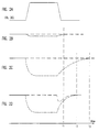
- Figure 2 is a timing diagram showing the voltage on the I/O data lines or memory read and write cycles.
- the column decode signal is shown by signal 2A defining the timing of a read or write cycle.
- Signal 2B shows the voltage on the I/O data lines during a read cycle
- signal 2C shows the voltage on the I/O data lines during a write cycle.
- a read operation can start at time t1 (signal 2B) when the data lines have equilibrated after a read cycle. After a write cycle, however, because the voltage differential is much greater, a read operation can not cccur until a considerably later time t3 (signal 2C) when equilibration occurs.
- SRAM static random access memory
- One way to reduce the equilibration delay is to reduce the effective resistance value of the PMOS pull-up transistors 114. This reduces the RC time constant and speeds up the recovery of the low I/O data line.
- smaller resistance reduces the voltage differential that develops between the complementary data lines during a read cycle.
- the differential amplifier requires a minimum ⁇ V at its inputs. Given smaller effective pull-up resistance, to obtain a sufficiently large ⁇ V would require larger read currents.
- column decode transistors 110 must be made larger. Larger decode transistors 110, however, directly add to the parasitic capacitance on I/O data lines 108, causing the RC time constant to increase. This is therefore not a viable option.
- a modification to this approach uses large (low resistance) pull-up transistors for moderately fast equilibration, and turns off these transistors during the following read cycle.
- This approach uses significant area for the large transistors and requires very critical timing for turning off the large pull-up transistors.
- NMOS equilibration transistor 118 that shorts the two data lines together when turned on.
- the voltage on the recovering low data line reaches a high enough value such that the gate-to-source voltage of NMOS equilibration transistor 118 goes below a threshold voltage, equilibration transistor 118 turns itself off (even though its gate is still at VDD), at which point both data lines move toward VDD independently.
- Equilibration transistor 118 therefore turns off in time to avoid any interference with the differential voltage that will develop across the data lines due to the read operation. Equilibration transistor 118 can thus be large to obtain fast equilibration. This significantly reduces the equilibration delay since the voltage on the low data line rises faster while the voltage on the high data line drops somewhat toward the voltage on the low data line. This is illustrated by signal 2D of Figure 2 which shows the voltage on the I/O line moving toward the voltage on the I/O ⁇ line to equilibrate at time t2, earlier than time t3. However, there still remains a small differential voltage between the I/O lines throughout their exponential rise toward VDD. Thus, this reduction in the data line equilibration delay is still not enough for very high speed operation.
- the present invention provides a method and a circuit for fast equilibration of data lines following a write cycle in memory circuits.
- the present invention includes an equilibration transistor and furthermore momentarily disables the PMOS pull-up transistor coupled to the high data line during the recovery of the low data line after a write cycle.
- the high data line discharges through the data line equilibration transistor toward the rising low data line.
- the high data line PMOS pull-up transistor disabled the high data line is pulled down until either the low data line rises above the high data lane or until the equilibration transistor turns off.
- the rising low data line would eventually rise above the high data line if the high data line PMOS pull-up transistor were to remain off. But the PMOS pull-up transistor on the high data line is reactivated at the moment the rising voltage on the low data line reaches the voltage on the high data line. This allows the two data lines to thereafter charge up to VDD in unison.
- An alternate embodiment of the present invention momentarily turns on the NMOS pull-down transistor coupled to the high data line during write recovery of the low data line.
- the NMOS pull-down transistor 116T is normally turned on only for writing a logic "0" on the data line. But if turned on very briefly during data line recovery following write of a "1", it speeds up the equilibration process by lowering the voltage on the high (true) data line.
- the NMOS pull-down transistor is preferably turned on only for the amount of time required for the high data line to meet the recovering low data line.
- a third embodiment of the present invention combines the above two embodiments by momentarily turning off the PMOS pull-up transistor and turning on the NMOS pull-down transistor connected to the high data line during the recovery period.
- the present invention provides in a memory circuit having a first and a second complementary data lines, with a pull-up transistor and a pull-down transistor coupled to each of the data lines, a method of equilibrating the voltage on the complementary data lines after a write cycle which includes the steps of: (a) turning on the pull-up transistor coupled to the first data line carrying a logic low voltage; (b) shorting the complementary data lines together by activating an equilibration transistor; and (c) momentarily turning off the pull-up transistor coupled to the second data line carrying a logic high voltage.
- the present invention provides in a memory circuit having a first and a second complementary data lines, a circuit for equilibrating the voltage on the data lines including an equilibration transistor having a first and a second terminal respectively coupled to the first and second data lines, a first pull-up transistor and a first pull-down transistor coupled to the first data line, a second pull-up transistor and a second pull-down transistor coupled to the second data line, and control means coupled to the pull-up and pull-down transistors for turning off the pull-up transistor coupled to the first data line carrying a high logic level during the initial recovery from a write cycle of the second I/O data line.
- FIG. 3 shows the memory I/O control circuit according to one embodiment of the present invention.
- the I/O control circuit includes a PMOS pull-up transistor 300 and an NMOS pull-down transistor 302 connected to an I/O line, and a similar pair, PMOS 304 and NMOS 306, connected to an I/O ⁇ line.
- the circuit receives an array select signal AS as one input, an array select logically ANDed with write enable signal AS ⁇ W as another input and DIN and DIN ⁇ that supply the write data.
- the write data is in the form of a pulse (in this example a positive pulse) on either DIN or DIN ⁇ , and when not writing both DIN and DIN ⁇ are at the same level (in this example low).
- the array select signal when deselected allows both I/O and I/O ⁇ to float. This may be required for some array architectures but is not relevant to the equilibration technique being described herein, and will not be further described.
- the array select signal AS is asserted high when the array is selected for reading or writing, while AS ⁇ W is asserted only when writing in the selected array.
- the control circuit for the true I/O line includes a two-input NAND gate 308 that receives signals AS ⁇ W and DIN ⁇ at its inputs.
- the output of NAND 308, node 310 connects to the input of an inverter 312 whose output, node 314, drives the gate terminal of NMOS pull-down transistor 302.
- the I/O ⁇ control circuit includes a similar circuit, made up of NAND gate 316 and inverter 320 driving the gate terminal of NMOS pull-down transistor 306, with DIN substituted for DIN ⁇ as an input of NAND gate 316.
- the gate terminal of PMOS pull-up transistor 300, node 332 is driven by the output of a three-input NAND gate 324.
- a first input of NAND gate 324 connects to the array select signal AS, while a second input connects to the output of NAND gate 308, node 310.
- the third input at node 336 is driven by the output of a three-inverter delay chain 326.
- the input of three-inverter delay chain 326 connects to the output of inverter 320, node 322.
- the I/O control circuit further includes an NMOS equilibration transistor EQ whose source and drain terminals connect to I/O and I/O ⁇ , respectively.
- a two-input NOR gate 338 receives DIN and DIN ⁇ at its inputs, and an inverter 342 receives AS ⁇ W at its input.
- a second two-input NOR gate 340 receives the outputs of NOR gate 338 and inverter 342 at its inputs.
- the output of NOR gate 340 connects to the input of an inverter 344 whose output drives the gate terminal of NMOS transistor EQ.
- a PMOS transistor may be used as the equilibration transistor. In that case, the circuit driving the gate of the PMOS equilibration transistor would have an inverted logic as compared to that shown in Figure 3.
- the operation of the circuit will be described hereinafter.
- the signals AS ⁇ W, DIN and DIN ⁇ are at logic low level. This will result in a logic low level at the outputs of inverters 312 and 320.
- NMOS pull-down transistors 302 and 306 are turned off. If the array is selected (i.e., AS is asserted), all inputs of NAND gates 324 and 328 are at logic high level, causing a low output on nodes 332 and 334, and thereby turning on PMOS pull-up transistors 300 and 304.
- both NMOS pull-down transistors 302 and 306 are off and both PMOS pull-up transistors 300 and 304 are on, pulling both I/O lines up to the positive power supply VDD.
- the equilibration transistor EQ has a high voltage on its gate since all signals DIN, DIN ⁇ , and AS ⁇ W are low, but it is off since the source and drain terminals are at the same high voltage as the gate terminal.
- the negative pulse at node 318 also causes the output of three-input NAND gate 328 to go high for the duration of the pulse, turning off PMOS transistor 304 two gate delays (316 and 328) after t0. Representing each gate delay by ⁇ , I/O ⁇ is thus, pulled low at time t0+3 ⁇ (316, 328/320, and 304/306).
- NAND gate 308 With DIN ⁇ at logic low level, the output of NAND gate 308 (node 310) remains high, and the output of inverter 312 remains low. Thus, NMOS transistor 302 remains turned off. Of the three inputs to NAND gate 324, two remain high (AS and node 310). Three-inverter delay chain 326 inverts and delays the positive pulse at node 322 and applies it to the third input at node 336. Thus, NAND gate 324 receives a negative pulse at input 336, five gate delays after t0 (316, 320, and 326) at time t0+5 ⁇ . A positive pulse therefore arrives at the gate terminal of PMOS transistor 300 disconnecting I/O from VDD at time t0+6 ⁇ .
- NMOS transistor 306 turns off and PMOS transistor 304 turns on at time t1+2 ⁇ (316 and 328/320).
- I/O ⁇ starts to move toward VDD at time t1+3 ⁇ (316, 328/320, and 304/306).
- the time t1+3 ⁇ marks the start of the recovery or equilibration process.
- NMOS transistor EQ which was turned off at time t0+3 ⁇ , remains off for the duration of the DIN pulse, and is turned back on at time t1+3 ⁇ (338, 340, 344).
- the equilibration transistor is therefore turned on at the same time (t1+3 ⁇ ) that I/O ⁇ starts to recover, moving from ground up toward VDD.
- equilibration transistor EQ shorting I/O to I/O ⁇ , the previously high I/O line moves down toward the recovering I/O ⁇ line as EQ helps PMOS transistor 304 pull the recovering I/O ⁇ line high.
- PMOS transistor 300 is turned off at this time. It is not turned back on until time t1+6 ⁇ (316, 320, 326, 324), pulling I/O up to VDD at time t1+7 ⁇ . As a result, PMOS transistor 300 is off for four gate delays (4 ⁇ ) after I/O ⁇ has started the equilibration process.
- PMOS pull-up transistor 300 is turned off allowing I/O to drop down toward rising I/O ⁇ .
- PMOS 300 is turned back on, after which both I/O and I/O ⁇ move toward VDD with the same time constant.
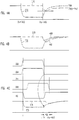
- the time at which PMOS 300 is turned back on (i.e., the length of time PMOS transistor 300 remains off after I/O ⁇ starts recovering) is very critical. This is shown in the timing diagram of Figure 4.
- Diagram 4A shows the behavior of the I/O lines when writing a logic "1" in the case where PMOS 300 is not turned on at all during recovery of the I/O ⁇ line. As explained above, at time t0+3 ⁇ , I/O ⁇ is pulled low to ground while I/O remains at VDD in order to write a logic "1" into an addressed memory cell coupled to the selected array.
- I/O ⁇ starts its recovery up toward VDD, while current through the equilibration transistor EQ causes I/O to drop toward I/O ⁇ . If PMOS 300 is not turned back on after a short delay, I/O continues to equilibrate toward the voltage on I/O ⁇ , falling as long as I/O ⁇ is below the voltage of I/O and then rising after the voltage on I/O ⁇ exceeds the voltage on I/O. After the voltage on I/O ⁇ exceeds the voltage on I/O, both I/O lines are pulled toward VDD by PMOS 304, I/O ⁇ directly and I/O through equilibration transistor EQ.
- Diagram 4B illustrates the cases where PMOS transistor 300 is turned on before and after the optimum time in the same diagram.
- PMOS 300 When PMOS 300 is turned on too early, it starts to pull I/O up toward VDD before I/O reaches I/O ⁇ (i.e., while I/O is still above I/O ⁇ ). This is shown by line 400.
- line 402. In either case, a differential voltage is maintained across the I/O lines as they approach VDD. Note that an identical resistor/capacitor loading on the I/O lines results in equal RC time constants for the signals on the I/O lines.
- Diagram 4C illustrates the timing of the control signals for the pull-up and pull-down transistors as well as the equilibration transistor coupled to the I/O lines and the signal on I/O lines when writing a logic "1".
- the gate terminals of the pull-up and pull-down transistors 304 and 306 i.e., nodes 334 and 322 are pulled low, ending the write cycle and beginning the data line equilibration process.
- the gate terminal of the equilibration transistor EQ is pulled high to turn on transistor EQ.
- the gate terminal of the NMOS pull-down transistor 302 (node 314) remains low keeping the pull down transistor off.
- the gate terminal of pull-up transistor 300 (node 332) is high during the write pulse, disconnecting I/O from VDD, and remains high during the initial phase of recovery.
- I/O rapidly drops down toward the recovering I/O ⁇ .
- about four gate delays later (time t n +4 ⁇ ) when the I/O lines intersect node 332 is pulled low turning on pull-up transistor 300. From that point on, both I/O lines are pulled up by their respective pull-up transistors with identical rise times. Thus, equilibration is achieved and maintained as soon as the voltage on the data lines intersect.
- the PMOS pull-up transistor connected to the high data line is turned off as in the first embodiment, and the NMOS pull-down transistor is turned on as in the second embodiment, simultaneously. Circuits similar to that shown in Figure 3 can be developed to realize these alternative embodiments.
- the polarities of the signals in the embodiment described are determined by the type of transistor used for the column decode transistors (110 in Figure 1) in a DRAM device, or memory cell access transistors in an SRAM device. That is, since the embodiment described in connection with Figure 3 assumes NMOS column decode transistors, the data lines are equilibrated at VDD. To write a logic "0" for example, the true data line (I/O) is pulled low, while its complement remains at VDD. However, if the column decode transistors (or memory cell access transistors in case of an SRAM) were PMOS type transistors, the data lines would be equilibrated at ground (or negative power supply voltage VSS).
- the present invention provides several embodiments for a method and a circuit for fast equilibration of data lines following a write cycle in memory circuits.
- An I/O control circuit separately controls the gate terminals of pull-up and pull-down transistors that are connected to the data lines. By separately controlling the on/off timing of these devices in such a way as to lower the voltage on the high data line, the circuit of the present invention achieves a data line equilibration time after a write cycle that can be even faster than that after a read cycle.
- the I/O control circuit described is based on a DRAM circuit
- a similar circuit can be used in an SRAM device where data input and output typically take place on the same set of data lines.
- the circuit for an SRAM is similar to that shown in Figure 1 without the memory cells 100, if one considers sense amplifier 105 as the SRAM memory cell flip-flop, decode transistors 110 as SRAM cell access transistors, and I/O data lines 108 as SRAM bit lines.
- sense amplifier 105 as the SRAM memory cell flip-flop
- decode transistors 110 as SRAM cell access transistors
- I/O data lines 108 as SRAM bit lines.
Landscapes
- Engineering & Computer Science (AREA)
- Databases & Information Systems (AREA)
- Microelectronics & Electronic Packaging (AREA)
- Computer Hardware Design (AREA)
- Static Random-Access Memory (AREA)
- Dram (AREA)
Applications Claiming Priority (4)
| Application Number | Priority Date | Filing Date | Title |
|---|---|---|---|
| US438148 | 1982-10-29 | ||
| US08/297,723 US5453951A (en) | 1994-08-26 | 1994-08-26 | Fast voltage equilibration of complementary data lines following write cycle in memory circuits |
| US297723 | 1994-08-26 | ||
| US08/438,148 US5546338A (en) | 1994-08-26 | 1995-05-09 | Fast voltage equilibration of differential data lines |
Publications (2)
| Publication Number | Publication Date |
|---|---|
| EP0701257A2 true EP0701257A2 (fr) | 1996-03-13 |
| EP0701257A3 EP0701257A3 (fr) | 1998-02-11 |
Family
ID=26970287
Family Applications (1)
| Application Number | Title | Priority Date | Filing Date |
|---|---|---|---|
| EP95113109A Ceased EP0701257A3 (fr) | 1994-08-26 | 1995-08-21 | Equilibration rapide de tension de lignes complémentaires de données après un cycle d'écriture pour circuits de mémoire |
Country Status (5)
| Country | Link |
|---|---|
| US (1) | US5546338A (fr) |
| EP (1) | EP0701257A3 (fr) |
| JP (1) | JPH08180679A (fr) |
| KR (1) | KR960008842A (fr) |
| CN (1) | CN1139810A (fr) |
Families Citing this family (19)
| Publication number | Priority date | Publication date | Assignee | Title |
|---|---|---|---|---|
| US5732036A (en) * | 1997-02-14 | 1998-03-24 | Micron Technology, Inc. | Memory device communication line control |
| US5923603A (en) * | 1997-08-20 | 1999-07-13 | Micron Technology, Inc. | Equilibrate circuit for dynamic plate sensing memories |
| US5978307A (en) * | 1998-05-21 | 1999-11-02 | Integrated Device Technology, Inc. | Integrated circuit memory devices having partitioned multi-port memory arrays therein for increasing data bandwidth and methods of operating same |
| US5999478A (en) * | 1998-05-21 | 1999-12-07 | Integrated Device Technology, Inc. | Highly integrated tri-port memory buffers having fast fall-through capability and methods of operating same |
| US6216205B1 (en) | 1998-05-21 | 2001-04-10 | Integrated Device Technology, Inc. | Methods of controlling memory buffers having tri-port cache arrays therein |
| US5982700A (en) * | 1998-05-21 | 1999-11-09 | Integrated Device Technology, Inc. | Buffer memory arrays having nonlinear columns for providing parallel data access capability and methods of operating same |
| US6031776A (en) * | 1999-08-17 | 2000-02-29 | United Microelectronics Corp. | Sense amplifier circuit for a semiconductor memory device |
| US6108257A (en) * | 1999-09-30 | 2000-08-22 | Philips Electronics North America Corporation | Zero power SRAM precharge |
| KR20020069656A (ko) * | 2001-02-27 | 2002-09-05 | 박종현 | 원단확포기의 원단꼬임 방지장치 |
| KR20020078007A (ko) * | 2001-04-04 | 2002-10-18 | 박종현 | 영상인식센서를 이용한 원단확포장치 |
| KR20030013031A (ko) * | 2001-08-06 | 2003-02-14 | 박종현 | 원단확포기의 원단 공급.인출 안내장치 |
| KR20030013002A (ko) * | 2001-08-06 | 2003-02-14 | 박종현 | 회전장치가 부설된 원단이송용 캐리어 |
| KR100447485B1 (ko) * | 2002-06-27 | 2004-09-07 | 장익순 | 오픈 콤팩터 폴딩작업의 리프팅장치 |
| KR100447483B1 (ko) * | 2002-06-27 | 2004-09-07 | 장익순 | 오픈 콤팩터의 원단중량 감지장치 |
| KR100447484B1 (ko) * | 2002-06-27 | 2004-09-07 | 장익순 | 오픈 콤팩터의 폴딩작업시 원단말림 방지장치 |
| US7424003B2 (en) * | 2004-03-08 | 2008-09-09 | Surf Communication Solutions | Multi-parameter scheduling in communication systems |
| KR100932724B1 (ko) * | 2005-09-09 | 2009-12-21 | 후지쯔 마이크로일렉트로닉스 가부시키가이샤 | 반도체 집적 회로 |
| US8588020B2 (en) * | 2011-11-16 | 2013-11-19 | United Microelectronics Corporation | Sense amplifier and method for determining values of voltages on bit-line pair |
| CN106940683B (zh) * | 2016-01-04 | 2018-12-28 | 综合器件技术公司 | 用于上电时的单端存储器信号均衡的方法和装置 |
Family Cites Families (11)
| Publication number | Priority date | Publication date | Assignee | Title |
|---|---|---|---|---|
| JPS6180589A (ja) * | 1984-09-26 | 1986-04-24 | Hitachi Ltd | ダイナミツク型ram |
| US4689771A (en) * | 1986-03-03 | 1987-08-25 | Motorola, Inc. | Memory with improved write mode to read mode transition |
| KR890003488B1 (ko) * | 1986-06-30 | 1989-09-22 | 삼성전자 주식회사 | 데이터 전송회로 |
| US5126974A (en) * | 1989-01-20 | 1992-06-30 | Hitachi, Ltd. | Sense amplifier for a memory device |
| JPH02252192A (ja) * | 1989-03-24 | 1990-10-09 | Hitachi Ltd | 半導体記憶装置 |
| JP2545481B2 (ja) * | 1990-03-09 | 1996-10-16 | 富士通株式会社 | 半導体記憶装置 |
| KR920010345B1 (ko) * | 1990-06-30 | 1992-11-27 | 삼성전자 주식회사 | 선충전수단을 구비한 라이트 드라이버(write driver) |
| US5250854A (en) * | 1991-11-19 | 1993-10-05 | Integrated Device Technology, Inc. | Bitline pull-up circuit operable in a low-resistance test mode |
| KR950000496B1 (ko) * | 1992-01-30 | 1995-01-24 | 삼성전자 주식회사 | 반도체 메모리 장치의 데이타 출력회로 |
| JPH0660665A (ja) * | 1992-08-10 | 1994-03-04 | Nec Corp | 半導体スタティックramのビット線負荷回路 |
| JP2906957B2 (ja) * | 1993-12-15 | 1999-06-21 | 日本電気株式会社 | 半導体メモリ装置 |
-
1995
- 1995-05-09 US US08/438,148 patent/US5546338A/en not_active Expired - Lifetime
- 1995-08-21 EP EP95113109A patent/EP0701257A3/fr not_active Ceased
- 1995-08-24 CN CN95115594A patent/CN1139810A/zh active Pending
- 1995-08-25 JP JP21715395A patent/JPH08180679A/ja active Pending
- 1995-08-25 KR KR1019950027366A patent/KR960008842A/ko not_active Abandoned
Non-Patent Citations (1)
| Title |
|---|
| None |
Also Published As
| Publication number | Publication date |
|---|---|
| JPH08180679A (ja) | 1996-07-12 |
| EP0701257A3 (fr) | 1998-02-11 |
| US5546338A (en) | 1996-08-13 |
| KR960008842A (ko) | 1996-03-22 |
| CN1139810A (zh) | 1997-01-08 |
Similar Documents
| Publication | Publication Date | Title |
|---|---|---|
| US5546338A (en) | Fast voltage equilibration of differential data lines | |
| EP0043245B1 (fr) | Mémoire statique à accès aléatoire équilibrée et préchargée de façon asynchrone | |
| US5455802A (en) | Dual dynamic sense amplifiers for a memory array | |
| US5973972A (en) | Precharge system for a semiconductor memory device | |
| US4813022A (en) | Static memory with pull-up circuit for pulling-up a potential on a bit line | |
| KR100487098B1 (ko) | 센스증폭기타이밍회로 | |
| EP0398245B1 (fr) | Mémoire à accès aléatoire de type dynamique | |
| JPH05290581A (ja) | プレチャージ用出力ドライバ回路 | |
| US5070482A (en) | Static random access memory | |
| JPH10188571A (ja) | 半導体メモリ回路装置及び半導体メモリセルの書き込み方法 | |
| US4829483A (en) | Method and apparatus for selecting disconnecting first and second bit line pairs for sensing data output from a drain at a high speed | |
| JPH04248193A (ja) | 個別的ビットライン回復回路 | |
| EP0085436A2 (fr) | Circuits tampons | |
| US5751160A (en) | Output buffer with improved operational speed and transitional current | |
| US4939691A (en) | Static random access memory | |
| US4815040A (en) | Static memory using a MIS field effect transistor | |
| US5453951A (en) | Fast voltage equilibration of complementary data lines following write cycle in memory circuits | |
| US6067264A (en) | High speed semiconductor memory device | |
| EP0475118A2 (fr) | Circuit amplificateur à miroir de courant et sa méthode d'entraînement | |
| US5327317A (en) | Self-terminating data line driver | |
| EP0453759B1 (fr) | Amplificateur CMOS régénératif sensible avec rétroaction à haute vitesse | |
| KR20020032394A (ko) | 반도체 메모리 소자 및 그의 쓰기 구동 방법 | |
| JPH0935476A (ja) | 可変プレート電圧発生回路を具備する半導体メモリ装置 | |
| US5239237A (en) | Control circuit having outputs with differing rise and fall times | |
| JPH0547178A (ja) | 高速センシング装置を具備した半導体メモリー装置 |
Legal Events
| Date | Code | Title | Description |
|---|---|---|---|
| PUAI | Public reference made under article 153(3) epc to a published international application that has entered the european phase |
Free format text: ORIGINAL CODE: 0009012 |
|
| AK | Designated contracting states |
Kind code of ref document: A2 Designated state(s): DE GB NL |
|
| PUAL | Search report despatched |
Free format text: ORIGINAL CODE: 0009013 |
|
| AK | Designated contracting states |
Kind code of ref document: A3 Designated state(s): DE GB NL |
|
| 17P | Request for examination filed |
Effective date: 19980717 |
|
| 17Q | First examination report despatched |
Effective date: 20000208 |
|
| GRAG | Despatch of communication of intention to grant |
Free format text: ORIGINAL CODE: EPIDOS AGRA |
|
| STAA | Information on the status of an ep patent application or granted ep patent |
Free format text: STATUS: THE APPLICATION HAS BEEN REFUSED |
|
| 18R | Application refused |
Effective date: 20011011 |