EP0701282A2 - Verbindungsstruktur mit reduzierter lokaler Spitzenstromdichte und Verfahren zum Herstellen einer Verbindungsschicht in einem Halbleiterbauelement - Google Patents
Verbindungsstruktur mit reduzierter lokaler Spitzenstromdichte und Verfahren zum Herstellen einer Verbindungsschicht in einem Halbleiterbauelement Download PDFInfo
- Publication number
- EP0701282A2 EP0701282A2 EP95111164A EP95111164A EP0701282A2 EP 0701282 A2 EP0701282 A2 EP 0701282A2 EP 95111164 A EP95111164 A EP 95111164A EP 95111164 A EP95111164 A EP 95111164A EP 0701282 A2 EP0701282 A2 EP 0701282A2
- Authority
- EP
- European Patent Office
- Prior art keywords
- interconnect
- interconnect level
- fingers
- interlevel connector
- interlevel
- Prior art date
- Legal status (The legal status is an assumption and is not a legal conclusion. Google has not performed a legal analysis and makes no representation as to the accuracy of the status listed.)
- Withdrawn
Links
Images

Classifications
-
- H—ELECTRICITY
- H10—SEMICONDUCTOR DEVICES; ELECTRIC SOLID-STATE DEVICES NOT OTHERWISE PROVIDED FOR
- H10W—GENERIC PACKAGES, INTERCONNECTIONS, CONNECTORS OR OTHER CONSTRUCTIONAL DETAILS OF DEVICES COVERED BY CLASS H10
- H10W20/00—Interconnections in chips, wafers or substrates
- H10W20/40—Interconnections external to wafers or substrates, e.g. back-end-of-line [BEOL] metallisations or vias connecting to gate electrodes
- H10W20/41—Interconnections external to wafers or substrates, e.g. back-end-of-line [BEOL] metallisations or vias connecting to gate electrodes characterised by their conductive parts
- H10W20/43—Layouts of interconnections
-
- H—ELECTRICITY
- H10—SEMICONDUCTOR DEVICES; ELECTRIC SOLID-STATE DEVICES NOT OTHERWISE PROVIDED FOR
- H10W—GENERIC PACKAGES, INTERCONNECTIONS, CONNECTORS OR OTHER CONSTRUCTIONAL DETAILS OF DEVICES COVERED BY CLASS H10
- H10W20/00—Interconnections in chips, wafers or substrates
- H10W20/40—Interconnections external to wafers or substrates, e.g. back-end-of-line [BEOL] metallisations or vias connecting to gate electrodes
- H10W20/41—Interconnections external to wafers or substrates, e.g. back-end-of-line [BEOL] metallisations or vias connecting to gate electrodes characterised by their conductive parts
- H10W20/435—Cross-sectional shapes or dispositions of interconnections
-
- Y—GENERAL TAGGING OF NEW TECHNOLOGICAL DEVELOPMENTS; GENERAL TAGGING OF CROSS-SECTIONAL TECHNOLOGIES SPANNING OVER SEVERAL SECTIONS OF THE IPC; TECHNICAL SUBJECTS COVERED BY FORMER USPC CROSS-REFERENCE ART COLLECTIONS [XRACs] AND DIGESTS
- Y10—TECHNICAL SUBJECTS COVERED BY FORMER USPC
- Y10S—TECHNICAL SUBJECTS COVERED BY FORMER USPC CROSS-REFERENCE ART COLLECTIONS [XRACs] AND DIGESTS
- Y10S257/00—Active solid-state devices, e.g. transistors, solid-state diodes
- Y10S257/92—Conductor layers on different levels connected in parallel, e.g. to reduce resistance
Definitions
- the present invention relates, in general, to semiconductor devices and, more particularly, to interconnect structures and methods of layout therefor that reduce electromigration at localized regions of high current density so that interconnect reliability is increased.
- Electromigration-related reliability failures continue to be a problem as semiconductor device geometries shrink into the sub-micron range and current densities within these devices continue to increase.
- electromigration-related reliability is becoming sufficiently critical that the two-dimensional design layout, and particularly the interconnect layout, of semiconductor devices is increasingly dictated in part by factors associated with the reduction of electromigration.
- Interconnect structures carrying high current density in prior semiconductor devices have exhibited electromigration failure at regions of high localized current density, such as at the edges joining aluminum interconnect runs to vias between multi-level interconnects, at contacts between metal interconnects, and in geometrical inhomogeneities in local, silicon substrate interconnect runs. Accordingly, it is desirable to have a semiconductor device with an interconnect layout structure that reduces premature failure due to electromigration at regions of high localized current density.
- the present invention provides an interconnect structure for reducing peak localized interconnect current density by distributing current flow around the perimeter of an interlevel connector in a semiconductor device.
- a first interconnect level is connected to a second interconnect level by the interlevel connector, and the perimeter of the interlevel connector is located at the juncture between the first interconnect level and the interlevel connector.
- the first interconnect level has two or more fingers protruding therefrom that connect to the perimeter of the interlevel connector. At least one opening in the first interconnect level is disposed between two of the fingers for dividing current flowing from the first interconnect level to the interlevel connector.
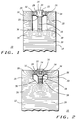
- FIG. 1 illustrates an interconnect structure 10 having an interconnect level 12 and an interlevel connector 14 connected thereto.
- Interconnect level 12 has three fingers 16, 18, and 20 protruding therefrom and connecting to interlevel connector 14.
- Interlevel connector 14 has a closed perimeter 22 comprising edges 24, 26, 28, and 30.
- Finger 16 has an extension 32 that connects to edge 28, finger 18 connects to edge 26, and finger 20 has an extension 34 that connects to edge 24.
- An opening 36 of interconnect level 12 is disposed between fingers 16 and 18, and an opening 38 is disposed between fingers 18 and 20.
- Interlevel connector 14 connects interconnect level 12 to a second interconnect level (not shown).
- interconnect level 12 In operation, current flows from interconnect level 12 through interlevel connector 14 to the second interconnect level (not shown). Specifically, current flow from interconnect level 12 is divided by fingers 16, 18 and 20. Opening 36 divides current flow between fingers 16 and 18, and opening 38 divides current flow between finger 18 and finger 20. Interconnect level 12 is patterned so that the current density in the regions near perimeter 22 of interlevel connector 14 (i.e. in each of fingers 16, 18, and 20 near perimeter 22) is substantially equal. Thus, extension 32, finger 18, and extension 34 have substantially equal current densities in the regions near connector 14.
- the patterning used for interconnect level 12 is selected to provide a resistance through each of fingers 16, 18 and 20, as measured from a common point of interconnect level 12 substantially distant from perimeter 22, that is substantially equal for each path. This ensures that these current paths are equally preferred and the current density in the regions near connector 14 is substantially equal in each of fingers 16, 18 and 20. If fingers 16, 18, and 20 are not equally-terminated (i.e. the cross-sectional areas of fingers 16, 18, and 20 are not equal) the resistance paths must be scaled in proportion to the fraction of this area for each of fingers 16, 18, and 20 to ensure proper current distribution in the region near connector 14, thus producing substantially equal current density within each of fingers 16, 18, and 20.
- Each of fingers 16, 18, and 20 has a major longitudinal axis that intersects interlevel connector 14.
- finger 16 has a longitudinal axis running through extension 32 which intersects interlevel connector 14.
- the longitudinal axis of each finger in FIG. 1 is separated by a radial rotation about interlevel connector 14 of about 90 o .
- this radial separation is at least 45 o .
- An advantage of the present invention is that current flow through interconnect level 12 is substantially distributed over a radial portion of perimeter 22 of preferably at least about 180 o .
- current flow is distributed over a radial portion of perimeter 22 of about 180 o .
- This is in contrast to previous interconnect structures having a single finger providing current to an interlevel connector through substantially a single edge thereof.
- Such current flow over a single edge resulted in pronounced current crowding at that edge.
- Current crowding is a localized region of high current density and typically results in premature failure from electromigration effects.
- the present invention avoids this problem by distributing current flow over more than one edge.
- the present invention may also be used with an interlevel connector having a more circular perimeter.
- a circular perimeter it is preferable that current flow be distributed over a radial portion of the perimeter of at least about 180 o , for example, about 270 o .
- current flow may be distributed over a full 360 o radius of the perimeter.
- interlevel connector 14 may be a tungsten via, and interconnect level 12 may be an aluminum interconnect level. Further, interlevel connector 14 may comprise one or more deposited (or grown) electrically-conductive layers, such as layers designed to diminish stress-migration and electromigration effects. Also, interconnect level 12 may comprise one or more deposited (or grown) electrically-conductive layers. One skilled in the art will recognize that the conductors used in connector 14 and interconnect level 12 may have layers composed of elemental, compound, alloy, or pseudo-alloy electrically-conductive materials.
- the second interconnect level may consist of a doped mono-crystalline silicon conductor, a local interconnect run in the underlying silicon substrate, or an extension of a CMOS or bipolar device structure as is typical in integrated circuits.
- Connector 14 may function primarily as the contact between the active devices formed in a mono-crystalline silicon substrate and the local poly-crystalline silicon or metal interconnect system.
- FIG. 2 illustrates an alternate interconnect structure 10 according to the first embodiment of the present invention.
- Common reference numbers from FIG. 1 are used for common elements in FIG. 2.
- FIG. 2 shows the effect of a different layout topology on the current density distribution in fingers 16, 18, and 20 (and in extensions 32 and 34) as well as the current density in the regions near the edge of the interlevel connector 14.
- the dimensions of that portion of interconnect level 12 immediately surrounding connector 14 may be made larger relative to the dimensions of connector 14 to improve the radial uniformity of current flow to an extent approaching 360° while also allowing greater tolerance for relative misalignment of interconnect level 12. Decreasing the overall geometrical size of interlevel connector 14 may also provide a significant advantage in the number of interconnect structures 10 possible within the layout of an integrated circuit, thus greatly reducing the likelihood of electromigration-induced early failures.
- a second embodiment of the present invention provides a method for fabricating an interconnect level in a semiconductor device to reduce the electromigration failure rate of the interconnect level.
- This method comprises the steps of selecting a preferred polycrystalline material to use in forming the interconnect level, and determining a median grain size (D50) for the polycrystalline material.
- D50 median grain size
- a first point and a second point of the semiconductor device are selected for electrical connection by the interconnect level, and these points are connected using essentially only a plurality of branches of the interconnect level wherein each of the branches has a linewidth less than the median grain size previously determined.
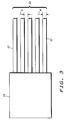
- FIG. 3 illustrates a two-dimensional layout of an interconnect level 50.
- Interconnect level 50 comprises a plurality of branches 52 connected to a current source 54.
- Branches 52 may be for example aluminum interconnect lines, and current source 54 may be for example a bonding pad.
- the linewidth of each of branches 52 is indicated as "W” in FIG. 3, and the separation between each of branches 52 is indicated as "S".
- the median grain size is a statistical quantity representing a figure of merit for the size of conductor grains and can be derived from any one or more of a number of accepted measurement methodologies.
- the generic method involves repeated measurements of the spatial dimensions of conductor grains and subsequent determination of a statistical figure of merit, which is a function of the distribution of the measured dimension and appropriate assumptions made about the nature of the distribution.
- this median grain size is a measured characteristic dependent on (1) the method of deposition, (2) the condition of the surface onto which the material is deposited, (3) the composition of the surface onto which the material is deposited, and (4) the subsequent thermal history after deposition for the conductors forming the interconnect structure.
- These factors (1),(2),(3), and (4) comprise a so-called “deposition process” and can be adjusted as desired to achieve various grain sizes and distributions.
- the optimal line dimensions (“W” and "S” in FIG. 3) are established after this deposition process is determined.
- branches 52 The reliability of branches 52 is enhanced when the lines are sized to achieve a so-called bamboo structure, a characteristic in which the median grain size is significantly larger than the linewidth.
- a bamboo structure in narrow lines is structurally different from that for wide polycrystalline lines.
- the bamboo structure characteristically has single-conductor grains connected serially, and separated by grain boundaries oriented along the transverse linewidth dimension and (extending directly through the lines to the supporting substrate).
- wide polycrystalline lines possessing linewidths larger than the median grain size have a large number of boundaries oriented in the direction of electron current flow.
- electromigration is a diffusion phenomena in which material transport occurs preferentially in the direction of electron current flow. Material flow for lines that are significantly wider than the median grain size is dominated by grain boundary diffusion, which tends to result in shorter lifetimes because a large number of boundaries are oriented along the direction of electron current flow.
- a plurality of grain boundaries for each of branches 52 is oriented perpendicular to the direction of electron current flow. This limits the material flow by diffusion processes in the direction of electron current flow along grain boundaries and confines the material flow to inter-grain (lattice) diffusion, which is significantly slower than grain boundary diffusion. As a result, electromigration transport is reduced and reliability is increased.
- This embodiment of the present invention can generally be used to connect any two points in a semiconductor device regardless of the distance between the two points or the current to be carried by the interconnect therebetween.
- the present invention is more advantageous when this distance is at least about 50 microns and the current density in each of the interconnect branches will exceed about 0.9 x 10⁵ A/cm2.
- polycrystalline materials such as for example polysilicon or aluminum-based conductors.
- a typical median grain size is about 1.7 microns
- a typical linewidth of branches 52 is preferably less than about 0.9 microns.
- the aforementioned case is only for illustrative purposes, and as mentioned previously, the median grain size (and resulting optimal linewidth and space for FIG. 3) will vary for differing deposition processes.
- this embodiment of the present invention will improve the process of heat transfer from interconnect level 50 to the underlying substrate (not shown) by virtue of the smaller thermal foot print of each of branches 52 in the structure relative to a single wide line of a comparable width equal to a combined number of parallel branches 52.
- the present invention provides an interconnect run between a first point and a second point in a semiconductor device that reduces electromigration failure.
- This interconnect run consists essentially of a plurality of upper straps connected to a plurality of lower straps by a plurality of interlevel connectors.
- Each of the upper straps is connected to two of the lower straps, and each of the lower straps is connected to two of the upper straps, forming a chain for substantially the full length from the first point to the second point.
- none of the upper straps or the lower straps has a length greater than, for example, about 12 microns and the interlevel connectors are formed of a material substantially resistant to electromigration, as in for example tungsten-filled plugs.
- FIG. 4 illustrates a cross-section of an interconnect run 60 having a plurality of upper straps 62 connected to a plurality of lower straps 64 by a plurality of interlevel connectors 66.
- the length of either one of upper straps 62 or lower straps 64 is substantially measured by the length (indicated as "L" in FIG. 4) from the center of one interlevel connector 66 to the next consecutive interlevel connector.
- interconnect run 60 when interlevel connectors 66 are formed of a material that does not exhibit electromigration, the material used to form upper straps 62 and lower straps 64 tends to move freely away from its interface with interlevel connectors 66, thus leading to electromigration failures. This phenomenon is seen, for example, where upper and lower straps 62 and 64 are both formed of aluminum and interlevel connectors 66 are tungsten. It has been discovered, however, if the length of each of straps 62 and 64 is reduced sufficiently, then a counter-migration of interconnect atoms will occur in the opposite direction to the electromigration flow. This counter-migration is the result of compressive stress, and ultimately leads to a desirable non-flow condition as described below.
- interconnect structures are encapsulated in isolating materials which completely encompass the interconnect structure.
- electromigration accelerating conditions e.g. electrical current and temperature
- material is displaced in the interconnect structure due to the applied current and temperature.
- the state of the interconnect structure changes in a time dependent manner as a result of this electromigration-induced material flow, becoming more mechanically tensile in areas where the material is flowing away from (cathode regions) and more mechanically compressive in areas where the material is flowing towards (anode regions).
- an anode region e.g.
- the mechanically-compressive stress increases and tends to retard further material flow into that region. Once a critical level of mechanical stress is reached, no further flow of material into that region is possible. After a sufficient period of time, like non-flow regions extend along interconnect run 60 and provide a static condition in which substantially no additional material will flow (even in the presence of current and thermal stress). This non-flow condition prevents further electromigration so that reliability is increased.
- the length of straps 62 and 64 is selected to be sufficiently small to accomplish this condition.
- the strap length "L" be less than for example about 12 microns, but this will vary depending on the particular deposition process used to form interconnect run 60. Also, this embodiment is more advantageous when the full length of interconnect run 60 is more than for example about 80 microns, again depending on the deposition process.
- interlevel connector 66 may be a via comprising tungsten
- upper and lower straps 62 and 64 may comprise aluminum
- the strap length may be less than about 6 microns.
- the lengths mentioned here and above may vary depending on the factors discussed above.
Landscapes
- Internal Circuitry In Semiconductor Integrated Circuit Devices (AREA)
- Design And Manufacture Of Integrated Circuits (AREA)
- Semiconductor Integrated Circuits (AREA)
Applications Claiming Priority (2)
| Application Number | Priority Date | Filing Date | Title |
|---|---|---|---|
| US08/283,338 US5461260A (en) | 1994-08-01 | 1994-08-01 | Semiconductor device interconnect layout structure for reducing premature electromigration failure due to high localized current density |
| US283338 | 1999-03-31 |
Publications (2)
| Publication Number | Publication Date |
|---|---|
| EP0701282A2 true EP0701282A2 (de) | 1996-03-13 |
| EP0701282A3 EP0701282A3 (de) | 1996-10-30 |
Family
ID=23085559
Family Applications (1)
| Application Number | Title | Priority Date | Filing Date |
|---|---|---|---|
| EP95111164A Withdrawn EP0701282A3 (de) | 1994-08-01 | 1995-07-17 | Verbindungsstruktur mit reduzierter lokaler Spitzenstromdichte und Verfahren zum Herstellen einer Verbindungsschicht in einem Halbleiterbauelement |
Country Status (3)
| Country | Link |
|---|---|
| US (2) | US5461260A (de) |
| EP (1) | EP0701282A3 (de) |
| JP (1) | JPH0864771A (de) |
Families Citing this family (32)
| Publication number | Priority date | Publication date | Assignee | Title |
|---|---|---|---|---|
| US5985703A (en) * | 1994-10-24 | 1999-11-16 | Banerjee; Sanjay | Method of making thin film transistors |
| US5506450A (en) * | 1995-05-04 | 1996-04-09 | Motorola, Inc. | Semiconductor device with improved electromigration resistance and method for making the same |
| US5712510A (en) * | 1995-08-04 | 1998-01-27 | Advanced Micro Devices, Inc. | Reduced electromigration interconnection line |
| US5689139A (en) * | 1995-09-11 | 1997-11-18 | Advanced Micro Devices, Inc. | Enhanced electromigration lifetime of metal interconnection lines |
| JP2755239B2 (ja) * | 1995-11-25 | 1998-05-20 | 日本電気株式会社 | 半導体装置用パッケージ |
| US6904675B1 (en) | 1996-09-27 | 2005-06-14 | Hewlett-Packard Development, L.P. | Method of forming electrical interconnects having electromigration-inhibiting plugs |
| US6245996B1 (en) * | 1996-09-27 | 2001-06-12 | Compaq Computer Corporation | Electrical interconnect structure having electromigration-inhibiting segments |
| US5841688A (en) * | 1997-06-27 | 1998-11-24 | Texas Instruments Incorporated | Matched delay word line strap |
| US5891802A (en) * | 1997-07-23 | 1999-04-06 | Advanced Micro Devices, Inc. | Method for fabricating a metallization stack structure to improve electromigration resistance and keep low resistivity of ULSI interconnects |
| JP3500308B2 (ja) | 1997-08-13 | 2004-02-23 | インターナショナル・ビジネス・マシーンズ・コーポレーション | 集積回路 |
| US5963831A (en) * | 1998-05-22 | 1999-10-05 | United Microelectronics Corp. | Method of making an interconnect structure employing equivalent resistance paths to improve electromigration resistance |
| US5959360A (en) * | 1998-05-22 | 1999-09-28 | United Microelectronics Corp. | Interconnect structure employing equivalent resistance paths to improve electromigration resistance |
| JP3464933B2 (ja) * | 1999-03-25 | 2003-11-10 | Necエレクトロニクス株式会社 | 半導体用配線評価装置 |
| JP2000294639A (ja) * | 1999-04-09 | 2000-10-20 | Oki Electric Ind Co Ltd | 半導体装置 |
| US6337274B1 (en) | 1999-12-06 | 2002-01-08 | Micron Technology, Inc. | Methods of forming buried bit line memory circuitry |
| JP3819670B2 (ja) | 2000-04-14 | 2006-09-13 | 富士通株式会社 | ダマシン配線を有する半導体装置 |
| US6828223B2 (en) * | 2001-12-14 | 2004-12-07 | Taiwan Semiconductor Manufacturing Co. | Localized slots for stress relieve in copper |
| DE10221867B4 (de) * | 2002-05-15 | 2007-06-06 | Loroch Gmbh | Vorrichtung zur Handhabung von scheibenförmigen Gegenständen, insbesondere Sägeblättern |
| US6818996B2 (en) * | 2002-12-20 | 2004-11-16 | Lsi Logic Corporation | Multi-level redistribution layer traces for reducing current crowding in flipchip solder bumps |
| US7096450B2 (en) | 2003-06-28 | 2006-08-22 | International Business Machines Corporation | Enhancement of performance of a conductive wire in a multilayered substrate |
| US20050082677A1 (en) * | 2003-10-15 | 2005-04-21 | Su-Chen Fan | Interconnect structure for integrated circuits |
| WO2005048314A2 (en) * | 2003-11-12 | 2005-05-26 | Silicon Pipe, Inc. | Tapered dielectric and conductor structures and applications thereof |
| US7466021B2 (en) * | 2003-11-17 | 2008-12-16 | Interconnect Portfolio, Llp | Memory packages having stair step interconnection layers |
| US7253528B2 (en) * | 2005-02-01 | 2007-08-07 | Avago Technologies General Ip Pte. Ltd. | Trace design to minimize electromigration damage to solder bumps |
| US7414275B2 (en) * | 2005-06-24 | 2008-08-19 | International Business Machines Corporation | Multi-level interconnections for an integrated circuit chip |
| US7525152B2 (en) * | 2006-03-02 | 2009-04-28 | Freescale Semiconductor, Inc. | RF power transistor device with metal electromigration design and method thereof |
| WO2008070115A2 (en) * | 2006-12-05 | 2008-06-12 | Wispry, Inc. | Substrates with slotted metals and related methods |
| US8089160B2 (en) * | 2007-12-12 | 2012-01-03 | International Business Machines Corporation | IC interconnect for high current |
| US20100320558A1 (en) * | 2009-06-18 | 2010-12-23 | Hsien-Chang Chang | Circuit layout structure and method to scale down ic layout |
| US20110101534A1 (en) * | 2009-11-04 | 2011-05-05 | International Business Machines Corporation | Automated short length wire shape strapping and methods of fabricting the same |
| US8901738B2 (en) | 2012-11-12 | 2014-12-02 | International Business Machines Corporation | Method of manufacturing an enhanced electromigration performance hetero-junction bipolar transistor |
| FR3050570A1 (fr) * | 2016-04-21 | 2017-10-27 | Commissariat Energie Atomique | Structure d'interconnexion electrique multi-niveaux a distribution de densite de courant optimisee |
Family Cites Families (18)
| Publication number | Priority date | Publication date | Assignee | Title |
|---|---|---|---|---|
| US4438450A (en) * | 1979-11-30 | 1984-03-20 | Bell Telephone Laboratories, Incorporated | Solid state device with conductors having chain-shaped grain structure |
| US4352239A (en) * | 1980-04-17 | 1982-10-05 | Fairchild Camera And Instrument | Process for suppressing electromigration in conducting lines formed on integrated circuits by control of crystalline boundary orientation |
| US4812419A (en) * | 1987-04-30 | 1989-03-14 | Hewlett-Packard Company | Via connection with thin resistivity layer |
| JPH073840B2 (ja) * | 1987-08-31 | 1995-01-18 | 株式会社東芝 | 半導体集積回路 |
| DE68922767T2 (de) * | 1988-03-18 | 1995-09-28 | Fujitsu Ltd | Verbindungsstruktur zum Verbinden von Leitern in einem elektronischen Apparat. |
| JPH02192146A (ja) * | 1989-01-20 | 1990-07-27 | Toshiba Corp | 半導体装置 |
| US5243221A (en) * | 1989-10-25 | 1993-09-07 | At&T Bell Laboratories | Aluminum metallization doped with iron and copper to prevent electromigration |
| US5268329A (en) * | 1990-05-31 | 1993-12-07 | At&T Bell Laboratories | Method of fabricating an integrated circuit interconnection |
| JPH04196428A (ja) * | 1990-11-28 | 1992-07-16 | Seiko Epson Corp | 半導体装置の製造方法 |
| US5229647A (en) * | 1991-03-27 | 1993-07-20 | Micron Technology, Inc. | High density data storage using stacked wafers |
| JPH05152299A (ja) * | 1991-04-15 | 1993-06-18 | Hitachi Ltd | 配線構造体 |
| JPH05160292A (ja) * | 1991-06-06 | 1993-06-25 | Toshiba Corp | 多層パッケージ |
| JPH05315327A (ja) * | 1992-02-10 | 1993-11-26 | Tadahiro Omi | 半導体装置及びその製造方法 |
| US5355023A (en) * | 1992-06-05 | 1994-10-11 | Nippon Steel Corporation | Semiconductor device having conducting layers connected through contact holes |
| US5382831A (en) * | 1992-12-14 | 1995-01-17 | Digital Equipment Corporation | Integrated circuit metal film interconnect having enhanced resistance to electromigration |
| EP0609501B1 (de) * | 1993-01-20 | 1999-09-15 | Kabushiki Kaisha Toshiba | Metallisierung auf Aluminiumbasis für Halbleiterbauelement |
| US5669793A (en) * | 1994-06-24 | 1997-09-23 | Walton; William H. | Apparatus and method for propelling a water vehicle |
| US5559055A (en) * | 1994-12-21 | 1996-09-24 | Advanced Micro Devices, Inc. | Method of decreased interlayer dielectric constant in a multilayer interconnect structure to increase device speed performance |
-
1994
- 1994-08-01 US US08/283,338 patent/US5461260A/en not_active Expired - Lifetime
-
1995
- 1995-07-17 EP EP95111164A patent/EP0701282A3/de not_active Withdrawn
- 1995-07-21 JP JP7206772A patent/JPH0864771A/ja active Pending
-
1996
- 1996-10-15 US US08/729,200 patent/US5760476A/en not_active Expired - Fee Related
Also Published As
| Publication number | Publication date |
|---|---|
| US5760476A (en) | 1998-06-02 |
| JPH0864771A (ja) | 1996-03-08 |
| US5461260A (en) | 1995-10-24 |
| EP0701282A3 (de) | 1996-10-30 |
Similar Documents
| Publication | Publication Date | Title |
|---|---|---|
| US5461260A (en) | Semiconductor device interconnect layout structure for reducing premature electromigration failure due to high localized current density | |
| US6678951B2 (en) | Method of forming electrical interconnects having electromigration-inhibiting plugs | |
| JPH07245307A (ja) | 相互接続配線構造およびその形成方法 | |
| US7470613B2 (en) | Dual damascene multi-level metallization | |
| US7439173B2 (en) | Increasing electromigration lifetime and current density in IC using vertically upwardly extending dummy via | |
| US4812419A (en) | Via connection with thin resistivity layer | |
| US6111310A (en) | Radially-increasing core power bus grid architecture | |
| US6489684B1 (en) | Reduction of electromigration in dual damascene connector | |
| JP3415010B2 (ja) | 半導体装置 | |
| US5506450A (en) | Semiconductor device with improved electromigration resistance and method for making the same | |
| WO2001045165A1 (en) | Bonding pad and support structure and method for their fabrication | |
| US7732924B2 (en) | Semiconductor wiring structures including dielectric cap within metal cap layer | |
| US20060005902A1 (en) | Method for production of thin metal-containing layers having low electrical resistance | |
| US7655563B2 (en) | Method for preventing the formation of dentrites in a semiconductor | |
| US6346721B1 (en) | Integrated circuit having radially varying power bus grid architecture | |
| US5641993A (en) | Semiconductor IC with multilayered Al wiring | |
| US6904675B1 (en) | Method of forming electrical interconnects having electromigration-inhibiting plugs | |
| US6894393B1 (en) | Buried power bus utilized as a sinker for high current, high power semiconductor devices and a method for providing the same | |
| US9318414B2 (en) | Integrated circuit structure with through-semiconductor via | |
| US6998699B2 (en) | Redundant interconnect high current bipolar device and method of forming the device | |
| US6882053B1 (en) | Buried power buss utilized as a ground strap for high current, high power semiconductor devices and a method for providing the same | |
| KR100190074B1 (ko) | 금속배선층 구조 및 그 형성방법 | |
| US9761529B2 (en) | Advanced metallization for damage repair | |
| JPH0685078A (ja) | 半導体集積回路の多層配線構造 | |
| KR20000000886A (ko) | 금속배선저항을 낮춘 반도체 메모리 소자 |
Legal Events
| Date | Code | Title | Description |
|---|---|---|---|
| PUAI | Public reference made under article 153(3) epc to a published international application that has entered the european phase |
Free format text: ORIGINAL CODE: 0009012 |
|
| AK | Designated contracting states |
Kind code of ref document: A2 Designated state(s): DE GB NL |
|
| PUAL | Search report despatched |
Free format text: ORIGINAL CODE: 0009013 |
|
| AK | Designated contracting states |
Kind code of ref document: A3 Designated state(s): DE GB NL |
|
| 17P | Request for examination filed |
Effective date: 19970502 |
|
| 17Q | First examination report despatched |
Effective date: 19990119 |
|
| STAA | Information on the status of an ep patent application or granted ep patent |
Free format text: STATUS: THE APPLICATION IS DEEMED TO BE WITHDRAWN |
|
| 18D | Application deemed to be withdrawn |
Effective date: 20010915 |