EP0701324B1 - Steuerschaltung für takt-multiplizierer - Google Patents
Steuerschaltung für takt-multiplizierer Download PDFInfo
- Publication number
- EP0701324B1 EP0701324B1 EP94926369A EP94926369A EP0701324B1 EP 0701324 B1 EP0701324 B1 EP 0701324B1 EP 94926369 A EP94926369 A EP 94926369A EP 94926369 A EP94926369 A EP 94926369A EP 0701324 B1 EP0701324 B1 EP 0701324B1
- Authority
- EP
- European Patent Office
- Prior art keywords
- signal
- clock
- input signal
- amplitude
- input
- Prior art date
- Legal status (The legal status is an assumption and is not a legal conclusion. Google has not performed a legal analysis and makes no representation as to the accuracy of the status listed.)
- Expired - Lifetime
Links
- 238000001514 detection method Methods 0.000 claims description 17
- 230000003321 amplification Effects 0.000 claims description 13
- 238000003199 nucleic acid amplification method Methods 0.000 claims description 13
- 238000000034 method Methods 0.000 claims description 4
- 239000003990 capacitor Substances 0.000 description 11
- 230000005540 biological transmission Effects 0.000 description 3
- 230000003111 delayed effect Effects 0.000 description 3
- 238000010897 surface acoustic wave method Methods 0.000 description 3
- 230000001771 impaired effect Effects 0.000 description 2
- 238000003780 insertion Methods 0.000 description 2
- 230000037431 insertion Effects 0.000 description 2
- 238000002407 reforming Methods 0.000 description 2
- 230000006866 deterioration Effects 0.000 description 1
- 230000001939 inductive effect Effects 0.000 description 1
- 230000003287 optical effect Effects 0.000 description 1
Images


Classifications
-
- H—ELECTRICITY
- H03—ELECTRONIC CIRCUITRY
- H03K—PULSE TECHNIQUE
- H03K5/00—Manipulating of pulses not covered by one of the other main groups of this subclass
- H03K5/00006—Changing the frequency
Definitions
- This invention relates to a control circuit for an output clock of a clock multiplier used for optical transmission equipments and multiplexers in a digital transmission system. More specifically, it relates to a control circuit for clock multiplier capable, when a multiplied signal comes out at the output due to influences of noise or whatever even while no input signal is applied, of controlling the output signal.
- a clock multiplier may be required, for example, in a general digital system, when the speed of a main processing unit is set at V/x to get phase margin regarding the processing in a system, in which processing is implemented by the speed V at the input and by the speed V at the output.
- data To output from the system such a signal processed at the speed V/x as a signal with the speed V, data must be converted into data with the speed V on the basis of a clock multiplied x times of the clock having the speed V/x used for processing.
- a clock multiplier is required in the situations described above.
- a limiter amplifier is provided in order for restituting a loss occurring by when a signal is fed at the input terminal of the clock multiplier, a loss caused by an insertion of a band pass filter, and the like.
- a limiter amplifier having its gain of about 32 dB is typically used.
- input of noise may be amplified even where no input signal is applied.
- a signal having amplitude and frequency equivalent to the multiplied clock obtainable when an input signal is given can come out at the output terminal.
- Japanese Patent Unexamined Publication Sho No. 56-47,139 is known regarding control of an output clock.
- the control circuit shown in the Patent Publication has constitution that a circuit detecting signal loss and a gate circuit are inserted between the output of the regenerate clock signal and an output terminal.
- the gate circuit to be inserted is required to have high performance electrical characteristics, representatively, such as rise time.
- Such a gate circuit is expensive and costs so much.
- the number of connection points for high frequency signal increases in order to insert the gate circuit, thereby inducing waveforms of the clock signal to be impaired.
- a clock multiplier configured to receive an input signal comprising a clock signal and to output an output signal comprising a frequency-multiplied clock signal
- the clock multiplier comprising amplifier means for receiving an intermediate signal derived from the input signal and comparing the intermediate signal with a bias reference level, peak detection means for determining the amplitude of the input signal, comparator means for comparing the amplitude of the input signal with a first reference voltage, which is less than the amplitude of the clock signal and a switching means for providing the amplifier means with the bias reference level so as to permit or suppress amplification of the intermediate signal in dependence upon the comparison of the amplitude of the input signal and the first reference voltage.
- the switching means may be configured to select a maximum voltage level as the bias reference level when the input signal is less than the first reference voltage so as to suppress amplification of the intermediate signal.
- the switching means may be configured to select an open circuit when the input signal is greater than the first reference voltage and the amplifier means sets the bias reference level to a self-bias voltage so as to permit amplification of the intermediate signal.
- the switching means may comprise an analog switch circuit whose input is controlled by the output of the comparator means.
- a method of operating a clock multiplier comprising receiving an input signal that comprises a clock signal, outputting an output signal comprising a frequency-multiplied clock signal, comparing an intermediate signal derived from the input signal with a bias reference level, measuring the amplitude of the input signal, comparing the amplitude of the input signal with a first reference voltage, which is less than the amplitude of the clock signal and providing the amplifier means with the bias reference level so as to suppress or allow amplification of the intermediate signal depending on the outcome of the comparison.
- the providing of the bias reference level may comprise selecting a maximum voltage level when the input signal is less than the first reference voltage and supplying the maximum voltage level as the bias reference level to the amplifier means so as to suppress amplification of the intermediate signal.
- the providing of the bias reference level may comprise selecting an open circuit when the input signal is greater than the first reference voltage and, at the amplifier means, setting the bias reference level to a self-bias voltage so as to permit amplification of the intermediate signal.
- FIG. 1 is a control for clock multiplier according to the invention.
- Fig. 2 is a timing chart for the control circuit for clock multiplier in Fig. 1. A constitutional example of the clock multiplier is shown by a portion enclosed by a broken line in Fig. 1.
- An input terminal 1 is connected to a capacitor 2.
- the capacitor 2 is connected to a first limiter amplifier 3.
- a terminal 4 is an open side of the first limiter amplifier 3.
- An output of the first limiter amplifier 3 is connected to an exclusive-nor gate 6.
- a negative output of the first limiter amplifier 3 is connected to the exclusive-nor gate 6 through a delay line 5.
- An output of the exclusive-nor gate 6 is connected to a band pass filter 7.
- An output of the band pass filter 7 is connected to a second limiter amplifier 8.
- the second limiter amplifier 8 is connected to an output terminal 17 and an output terminal 18 fed with a signal reversed of the signal at the terminal 17.
- the input terminal 1 is connected to a peak detection circuit 9.
- the peak detection circuit 9 is connected to the comparator 10.
- a reference voltage input terminal 11 is also connected to the comparator 10.
- the comparator 10 is connected to an analog switch 12 through an input switching terminal 13.
- the analog switch 12 is formed with input terminals 14, 15.
- the analog switch 12 is further connected to the limiter amplifier 8 through a logic threshold reference terminal 16.
- a clock signal having a cycle 2T is fed at the input terminal 1.
- the waveform of the input signal A is shown by A in Fig. 2.
- the input signal indicated by A may have a smaller amplitude due to loss and the like during a step to be fed to the input terminal 1.
- the signal A is first fed to the capacitor 2 of the clock multiplier circuit to adjust its level.
- the output signal from the capacitor 2 is fed to the first limiter amplifier 3.
- the limiter amplifier is defined as an amplifier setting a limited value of an amplified signal.
- the limited amplifier here sets the limited value to the amplitude value of the signal to be fed.
- the amplitude of the signal A, impaired due to the loss is restituted by reforming the waveform at the first limiter amplifier 3.
- B in Fig. 2 shows a signal which restituted its amplitude from reforming its waveform.
- the signal B is fed to the exclusive-nor gate 6. If four times multiplying is considered, and if the cycle and the pulse width are set to 2T, T, respectively, the reverse signal C of the signal B is fed to the delay line 5, thereby being delayed by 1/4T cycle. In this control circuit for clock multiplier, if the number of multiplying times is set to N, the signal is delayed by (1/N)T.
- the signal D delayed at the delay line 5 is also fed to the exclusive-nor gate 6. Therefore, the signals B, D are fed to the exclusive-nor gate 6.
- a logic operation of exclusive-nor of the signals B, D is implemented at the exclusive-nor gate 6 and provides signal E.
- the waveform of the signal E is shown by E in Fig. 2.
- the signal E is fed to the band pass filter 7.
- the band pass filter 7 is constituted of a surface acoustic wave (SAW) filter.
- the band pass filter 7 can extract a necessary frequency signal of the multiplied clock.
- a waveform having a four times frequency is extracted, and then signal F is obtained.
- the waveform of the signal F as the output of the band pass filter 7 is shown by F in Fig. 2.
- the signal F as the multiplied signal of the input signal A has deteriorated waveform due to insertion loss of the SAW filter, electrical power loss when passing the band pass filter 7, or whatever. To restitute such losses, the output of the band pass filter 7 is fed to the second limiter amplifier 8.
- the second limiter amplifier 8 is also an amplifier similar to the first limiter amplifier 3, and sets the limited value of the amplified signal to an amplitude of a multiplied signal to be obtained.
- the second limiter amplifier 8 restitutes deteriorations of the waveform of the signal F.
- the signal A fed to the input terminal 1 is also fed to the capacitor 2 of the clock multiplier as well as to the peak detection circuit 9.
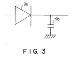
- the constitution of the peak detection circuit 9 is shown in Fig. 3.
- the peak detection circuit 9 in this embodiment is constituted of a diode 9a and a capacitor 9b.
- the diode 9a passes a signal having voltage of the forward bias or above of the diode 9a and does not pass a signal having voltage of the forward bias or below.
- a diode whose forward bias is less than the amplitude value of the input signal is used here as diode 9a.
- the diode 9a when a clock having a smaller amplitude than the forward bias of the diode 9a is fed, the signal cannot pass through it, so that zero level is obtained from the output of the peak detection circuit 9, and so that the circuit operates similarly when noise is applied as described below.
- the diode 9a and the capacitor 9b are formed for the peak detection circuit 9, the peak values can be detected by operation described below even if only capacitors constitute the peak detection circuit 9.
- the signal fed to the peak detection circuit 9, after passing the diode 9a, is gradually charged at the capacitor 9b up to the peak value of the amplitude. Now, if there is an input clock, it is charged up to the peak value of the amplitude of the signal A, and therefore, the peak detection circuit 9 detects the peak value.
- the peak value is fed to the comparator 10.
- the peak value of the amplitude is compared at the comparator 10 with the first reference voltage fed from the reference voltage input terminal 11.
- the first reference voltage is previously set to a value less than the amplitude of the clock signal to be fed.
- the comparator 10 output a signal of H level when the peak value of the amplitude as the output of the peak detection circuit 9 is greater than the first reference voltage, and output a signal of L level when less. Therefore, where there is an input clock, the peak value of the amplitude detected at the peak detection circuit 9 is always greater than the first reference voltage, so that the output of the comparator 10 becomes the signal of H level.
- the output signal of the comparator 10 is fed to the input switching terminal 13 of the analog switching circuit 12.
- the input terminal 14 When the signal fed to the input switching terminal 13 is at H level, the input terminal 14 is selected as the input of the analog switching circuit 12.
- the analog switching circuit 12 controls the value of the second reference voltage inside the second limiter amplifier 8 according to the value of the voltage of the input terminal to be connected.
- the analog switching circuit 12 is connected to the second limiter amplifier 8 through the logic threshold reference terminal 16.
- the second reference voltage controlled through the logic threshold reference terminal 16 falls in a condition that it is self-biased to the DC voltage of the second limiter amplitude 8.
- the second limiter amplifier 8 outputs a signal of H level when the input signal is greater than the second reference voltage, and outputs a signal of L level when the input signal is less.
- signal G restituting the loss in the signal F fed to the second limiter amplifier 8 is obtained at the output terminal 17 of the second limiter amplifier 8.
- Reverse signal H of the signal G is obtained at the output terminal 18.
- the waveforms of the signals G, H are shown by G, H, respectively, in Fig. 2.
- the clock output signal that the input signal is multiplied four times is thus obtained at the output terminals 17, 18.
- this noise is also fed to the portion of the control circuit.
- Noise having small amplitude is not recognized because of the diode 9a of the peak detection circuit 9.
- a portion at which its amplitude is large in the noise that passed through the diode 9a is charged at the capacitor 9b, it is little charged because the portion that no input is given to the capacitor 9b is long, and therefore, the value detected as the peak value at the peak detection circuit 9 is nearly zero level.
- This nearly zero level signal is compared at the comparator 10 with the first reference voltage at the reference voltage input terminal 11.
- the first reference voltage has a slightly less value than the value of the amplitude of the input clock signal, and is greater than the nearly zero level.
- the output of the comparator 10 becomes a signal of L level.
- the input terminal 15 is selected as the input of the analog switching circuit 12.
- the input terminal 15 is set to the maximum voltage level of the signal fed to the second limiter amplifier.
- the second reference voltage controlled through the logic threshold reference terminal 16 is therefore set to the maximum voltage level of the input signal of the second limiter amplifier.
- the signal F fed to the second limiter amplifier 8 is compared with the second reference voltage, the value of the signal F is always less than the second reference voltage. Therefore, a signal of L level as of information that the signal F is less than the second reference voltage is obtained as the output of the second limiter amplifier 8, and a stable signal of L level is obtained at the output terminal 17.
- the output signal can be controlled by, at the portion of the control circuit, detecting that there is no input signal and by comparing at the limiter amplifier with the reference voltage.
- the portion of the control circuit, used for the control circuit for clock multiplier can be used for control of output signals of receivers or the like except the clock multiplier.
- control circuit for clock multiplier is effectively used for high speed digital signal pressing equipments as optional transmission equipment, multiplier, switching system.
Landscapes
- Physics & Mathematics (AREA)
- Nonlinear Science (AREA)
- Control Of Amplification And Gain Control (AREA)
- Manipulation Of Pulses (AREA)
- Dc Digital Transmission (AREA)
- Tone Control, Compression And Expansion, Limiting Amplitude (AREA)
Claims (7)
- Taktmultiplizierer, der konfiguriert ist, ein Eingangssignal zu empfangen, das ein Taktsignal (A) umfaßt, und ein Ausgangssignal auszugeben, das ein frequenzmultipliziertes Taktsignal (G, H) umfaßt, wobei der Taktmultiplizierer folgendes umfaßt:eine Verstärkereinrichtung (8) zum Empfangen eines Zwischensignals (F), das von dem Eingangssignal abgeleitet wurde, und Vergleichen des Zwischensignals mit einem Vorspannungs-Referenzpegel (16);eine Spitzen-Detektionseinrichtung (9) zum Ermitteln der Amplitude des Eingangssignals;eine Komparatoreinrichtung (10) zum Vergleichen der Amplitude des Eingangssignals mit einer ersten Referenzspannung (11), die kleiner ist als die Amplitude des Taktsignals;
und gekennzeichnet ist durcheine Schalteinrichtung (12) zum Zuführen des Vorspannungs-Referenzpegels an die Verstärkereinrichtung, um die Verstärkung des Zwischensignals in Abhängigkeit vom Vergleich der Amplitude des Eingangssignals mit der ersten Referenzspannung zuzulassen oder zu unterdrücken. - Taktmultiplizierer nach Anspruch 1, bei dem die Schalteinrichtung (12) konfiguriert ist, einen maximalen Spannungspegel (15) als den Vorspannungs-Referenzpegel auszuwählen, wenn das Eingangssignal kleiner ist als die erste Referenzspannung, um die Verstärkung des Zwischensignals zu unterdrücken.
- Taktmultiplizierer nach Anspruch 1, bei dem die Schalteinrichtung (12) konfiguriert ist, einen offenen Stromkreis (14) auszuwählen, wenn das Eingangssignal größer als die erste Referenzspannung ist, und bei dem die Verstärkereinrichtung (8) den Vorspannungs-Referenzpegel auf eine Selbstvorspannung einstellt, um die Verstärkung des Zwischensignals zuzulassen.
- Taktmultiplizierer nach einem der vorhergehenden Ansprüche, bei dem die Schalteinrichtung (12) einen analogen Schaltkreis umfaßt, dessen Eingang durch den Ausgang (13) der Komparatoreinrichtung (10) gesteuert wird.
- Verfahren zum Betreiben eines Taktmultiplizierers, das folgendes umfaßt:Empfangen eines Eingangssignals, das ein Taktsignal (A) umfaßt;Ausgeben eines Ausgangssignals, das ein frequenzmultipliziertes Taktsignal (G, H) umfaßt;Vergleichen eines Zwischensignals (F), das vom Eingangssignal abgeleitet wurde, mit einem Vorspannungs-Referenzpegel;Messen (9) der Amplitude des Eingangssignals;Vergleichen (10) der Amplitude des Eingangssignals mit einer ersten Referenzspannung (11), die kleiner ist als die Amplitude des Taktsignals, undZuführen des Vorspannungs-Referenzpegels an die Verstärkereinrichtung (8), um in Abhängigkeit vom Ergebnis des Vergleichs die Verstärkung des Zwischensignals zuzulassen oder zu unterdrücken.
- Verfahren nach Anspruch 5, bei dem, wenn das Eingangssignal kleiner als die erste Referenzspannung ist, das Zuführen des Vorspannungs-Referenzpegels das Auswählen eines maximalen Spannungspegels (15) sowie das Anlegen des maximalen Spannungspegels als Vorspannungs-Referenzpegel an die Verstärkereinrichtung (8) umfaßt, um die Verstärkung des Zwischensignals zu unterdrücken.
- Verfahren nach Anspruch 5, bei dem, wenn das Eingangssignal größer ist als die erste Referenzspannung, das Zuführen des Vorspannungs-Referenzpegels das Auswählen eines offenen Stromkreises (14) und, an der Verstärkereinrichtung (8), das Einstellen des Vorspannungs-Referenzpegels auf eine Selbstvorspannung umfaßt, um die Verstärkung des Zwischensignals zuzulassen.
Applications Claiming Priority (4)
| Application Number | Priority Date | Filing Date | Title |
|---|---|---|---|
| JP23153893 | 1993-09-17 | ||
| JP23153893 | 1993-09-17 | ||
| JP231538/93 | 1993-09-17 | ||
| PCT/JP1994/001481 WO1995008217A1 (en) | 1993-09-17 | 1994-09-08 | Clock multiplying signal control circuit |
Publications (3)
| Publication Number | Publication Date |
|---|---|
| EP0701324A1 EP0701324A1 (de) | 1996-03-13 |
| EP0701324A4 EP0701324A4 (de) | 1997-05-28 |
| EP0701324B1 true EP0701324B1 (de) | 2000-12-27 |
Family
ID=16925072
Family Applications (1)
| Application Number | Title | Priority Date | Filing Date |
|---|---|---|---|
| EP94926369A Expired - Lifetime EP0701324B1 (de) | 1993-09-17 | 1994-09-08 | Steuerschaltung für takt-multiplizierer |
Country Status (4)
| Country | Link |
|---|---|
| US (1) | US5563538A (de) |
| EP (1) | EP0701324B1 (de) |
| CA (1) | CA2149511A1 (de) |
| WO (1) | WO1995008217A1 (de) |
Families Citing this family (6)
| Publication number | Priority date | Publication date | Assignee | Title |
|---|---|---|---|---|
| US5992966A (en) * | 1996-11-22 | 1999-11-30 | Canon Kabushiki Kaisha | Ink jet recording apparatus |
| JP3495239B2 (ja) * | 1998-01-12 | 2004-02-09 | 富士通株式会社 | クロック信号検出回路 |
| US6509766B1 (en) | 2001-10-26 | 2003-01-21 | International Business Machines Corporation | Adjustable clock multiplier and method |
| FR3009461B1 (fr) * | 2013-08-01 | 2015-08-07 | Thales Sa | Dispositif de protection d'au moins un composant actif d'un module electronique |
| CN112217536B (zh) * | 2020-11-30 | 2024-03-08 | 成都泰格微电子研究所有限责任公司 | 一种卫星地面站的射频前端及其自检方法 |
| CN119210367B (zh) * | 2024-11-29 | 2025-02-28 | 成都铭科思微电子技术有限责任公司 | 一种可切换不同倍频比输出的倍频放大链路 |
Family Cites Families (13)
| Publication number | Priority date | Publication date | Assignee | Title |
|---|---|---|---|---|
| US3710253A (en) * | 1971-03-29 | 1973-01-09 | Marconi Instruments Ltd | Performance checking and measuring devices and methods for signal channels |
| JPS5810885B2 (ja) * | 1974-04-19 | 1983-02-28 | 日本電気株式会社 | エンザンゾウフクキ ノ シユンジダンゾクカイロ |
| JPS5841694B2 (ja) * | 1974-07-02 | 1983-09-13 | 株式会社東芝 | ザツオンジヨキヨカイロ |
| JPS51130156A (en) * | 1975-05-06 | 1976-11-12 | Nec Corp | Frequency multiplier |
| GB1469374A (en) * | 1975-06-26 | 1977-04-06 | Burroughs Corp | Frequency-doubler circuit |
| JPS5647139A (en) * | 1979-09-25 | 1981-04-28 | Mitsubishi Electric Corp | Optical transmitting signal-break detecting circuit |
| JPS5841694A (ja) * | 1981-09-07 | 1983-03-10 | Kawasaki Steel Corp | サブマ−ジ溶接用焼成型フラツクス |
| JPS61173518A (ja) * | 1985-01-29 | 1986-08-05 | Nec Corp | 信号断検出回路 |
| JPS61224615A (ja) * | 1985-03-29 | 1986-10-06 | Toshiba Corp | クロツク信号周波数逓倍回路 |
| JPH031730A (ja) * | 1989-05-30 | 1991-01-08 | Sumitomo Electric Ind Ltd | 光送信回路 |
| JPH03136515A (ja) * | 1989-10-23 | 1991-06-11 | Nec Corp | 逓倍回路 |
| JP2808954B2 (ja) * | 1991-11-13 | 1998-10-08 | 国際電信電話株式会社 | 無変調信号検出及び周波数引き込み装置 |
| US5438245A (en) * | 1992-05-27 | 1995-08-01 | Sony Corporation | High-voltage generating circuit |
-
1994
- 1994-09-08 WO PCT/JP1994/001481 patent/WO1995008217A1/ja not_active Ceased
- 1994-09-08 US US08/433,323 patent/US5563538A/en not_active Expired - Lifetime
- 1994-09-08 EP EP94926369A patent/EP0701324B1/de not_active Expired - Lifetime
- 1994-09-08 CA CA002149511A patent/CA2149511A1/en not_active Abandoned
Also Published As
| Publication number | Publication date |
|---|---|
| EP0701324A1 (de) | 1996-03-13 |
| CA2149511A1 (en) | 1995-03-23 |
| US5563538A (en) | 1996-10-08 |
| EP0701324A4 (de) | 1997-05-28 |
| WO1995008217A1 (en) | 1995-03-23 |
Similar Documents
| Publication | Publication Date | Title |
|---|---|---|
| EP0720286B1 (de) | Ausgangssteuerschaltung für eine Übertragungsleistungsschaltung | |
| EP0016503A1 (de) | Wellenform-Korrektionsschaltung | |
| EP0543396A1 (de) | FM-Empfänger mit zwei Zwischenfrequenz-Band-Pass-Filtern | |
| EP0701324B1 (de) | Steuerschaltung für takt-multiplizierer | |
| JP2962218B2 (ja) | ディジタル光受信回路 | |
| US5378946A (en) | Arrangement for temporal detection of a signal edge of an electrical signal transmitted over a transmission line | |
| US7103122B2 (en) | Noise canceller | |
| EP0199602B1 (de) | Signalverarbeitungsschaltung | |
| US6337887B1 (en) | Burst receiving circuit and control method thereof | |
| EP0528689B1 (de) | Detektor | |
| US7366491B1 (en) | Noise cancel circuit | |
| JP2917178B2 (ja) | クロック逓倍信号制御回路 | |
| JP3044977B2 (ja) | ダイバシティアンテナ切換制御回路 | |
| JP3077154B2 (ja) | エンハンサ回路 | |
| JPS59224985A (ja) | ゴ−スト除去装置 | |
| JPH1048267A (ja) | ピーク検出回路 | |
| US4672428A (en) | Integrated digital gain control circuit for digital chrominance signals | |
| KR100243202B1 (ko) | 배속 변화에 상응한 직류 변동 신호 차단회로 | |
| JPWO1995008217A1 (ja) | クロック逓倍信号制御回路 | |
| JPS63304728A (ja) | 受信アンテナ切換/選択装置 | |
| JPH05292523A (ja) | 輪郭補正装置 | |
| JPS63175546A (ja) | デジタルデ−タ変換器 | |
| SU1317676A2 (ru) | Устройство слежени за задержкой шумоподобных сигналов | |
| JPH0225314B2 (de) | ||
| KR100276472B1 (ko) | 고화질 텔레비젼의 자동이득 제어방법 |
Legal Events
| Date | Code | Title | Description |
|---|---|---|---|
| PUAI | Public reference made under article 153(3) epc to a published international application that has entered the european phase |
Free format text: ORIGINAL CODE: 0009012 |
|
| 17P | Request for examination filed |
Effective date: 19950428 |
|
| AK | Designated contracting states |
Kind code of ref document: A1 Designated state(s): FR GB |
|
| A4 | Supplementary search report drawn up and despatched |
Effective date: 19970407 |
|
| AK | Designated contracting states |
Kind code of ref document: A4 Designated state(s): FR GB |
|
| 17Q | First examination report despatched |
Effective date: 19990726 |
|
| GRAG | Despatch of communication of intention to grant |
Free format text: ORIGINAL CODE: EPIDOS AGRA |
|
| GRAG | Despatch of communication of intention to grant |
Free format text: ORIGINAL CODE: EPIDOS AGRA |
|
| GRAH | Despatch of communication of intention to grant a patent |
Free format text: ORIGINAL CODE: EPIDOS IGRA |
|
| GRAH | Despatch of communication of intention to grant a patent |
Free format text: ORIGINAL CODE: EPIDOS IGRA |
|
| GRAA | (expected) grant |
Free format text: ORIGINAL CODE: 0009210 |
|
| AK | Designated contracting states |
Kind code of ref document: B1 Designated state(s): FR GB |
|
| ET | Fr: translation filed | ||
| PGFP | Annual fee paid to national office [announced via postgrant information from national office to epo] |
Ref country code: FR Payment date: 20010911 Year of fee payment: 8 |
|
| PGFP | Annual fee paid to national office [announced via postgrant information from national office to epo] |
Ref country code: GB Payment date: 20010912 Year of fee payment: 8 |
|
| PLBE | No opposition filed within time limit |
Free format text: ORIGINAL CODE: 0009261 |
|
| STAA | Information on the status of an ep patent application or granted ep patent |
Free format text: STATUS: NO OPPOSITION FILED WITHIN TIME LIMIT |
|
| 26N | No opposition filed | ||
| REG | Reference to a national code |
Ref country code: GB Ref legal event code: IF02 |
|
| PG25 | Lapsed in a contracting state [announced via postgrant information from national office to epo] |
Ref country code: GB Free format text: LAPSE BECAUSE OF NON-PAYMENT OF DUE FEES Effective date: 20020908 |
|
| GBPC | Gb: european patent ceased through non-payment of renewal fee |
Effective date: 20020908 |
|
| PG25 | Lapsed in a contracting state [announced via postgrant information from national office to epo] |
Ref country code: FR Free format text: LAPSE BECAUSE OF NON-PAYMENT OF DUE FEES Effective date: 20030603 |
|
| REG | Reference to a national code |
Ref country code: FR Ref legal event code: ST |