EP0702373B1 - Mémoire d'adresse redondante et sa méthode de test - Google Patents
Mémoire d'adresse redondante et sa méthode de test Download PDFInfo
- Publication number
- EP0702373B1 EP0702373B1 EP95305820A EP95305820A EP0702373B1 EP 0702373 B1 EP0702373 B1 EP 0702373B1 EP 95305820 A EP95305820 A EP 95305820A EP 95305820 A EP95305820 A EP 95305820A EP 0702373 B1 EP0702373 B1 EP 0702373B1
- Authority
- EP
- European Patent Office
- Prior art keywords
- address
- redundant
- line
- test
- redundant address
- Prior art date
- Legal status (The legal status is an assumption and is not a legal conclusion. Google has not performed a legal analysis and makes no representation as to the accuracy of the status listed.)
- Expired - Lifetime
Links
- 230000015654 memory Effects 0.000 title claims description 58
- 238000010998 test method Methods 0.000 title description 2
- 238000012360 testing method Methods 0.000 claims description 48
- 230000000295 complement effect Effects 0.000 claims description 5
- 238000010586 diagram Methods 0.000 description 4
- BDEDPKFUFGCVCJ-UHFFFAOYSA-N 3,6-dihydroxy-8,8-dimethyl-1-oxo-3,4,7,9-tetrahydrocyclopenta[h]isochromene-5-carbaldehyde Chemical compound O=C1OC(O)CC(C(C=O)=C2O)=C1C1=C2CC(C)(C)C1 BDEDPKFUFGCVCJ-UHFFFAOYSA-N 0.000 description 2
- 101000915578 Homo sapiens Zinc finger HIT domain-containing protein 3 Proteins 0.000 description 2
- 102100028598 Zinc finger HIT domain-containing protein 3 Human genes 0.000 description 2
- 239000000872 buffer Substances 0.000 description 2
- 230000002950 deficient Effects 0.000 description 2
- 230000003213 activating effect Effects 0.000 description 1
- 238000004458 analytical method Methods 0.000 description 1
- 230000009977 dual effect Effects 0.000 description 1
- 230000000694 effects Effects 0.000 description 1
- 230000006870 function Effects 0.000 description 1
- 230000004044 response Effects 0.000 description 1
Images
Classifications
-
- G—PHYSICS
- G11—INFORMATION STORAGE
- G11C—STATIC STORES
- G11C29/00—Checking stores for correct operation ; Subsequent repair; Testing stores during standby or offline operation
- G11C29/04—Detection or location of defective memory elements, e.g. cell constructio details, timing of test signals
- G11C29/08—Functional testing, e.g. testing during refresh, power-on self testing [POST] or distributed testing
- G11C29/12—Built-in arrangements for testing, e.g. built-in self testing [BIST] or interconnection details
- G11C29/18—Address generation devices; Devices for accessing memories, e.g. details of addressing circuits
- G11C29/24—Accessing extra cells, e.g. dummy cells or redundant cells
-
- G—PHYSICS
- G11—INFORMATION STORAGE
- G11C—STATIC STORES
- G11C29/00—Checking stores for correct operation ; Subsequent repair; Testing stores during standby or offline operation
- G11C29/04—Detection or location of defective memory elements, e.g. cell constructio details, timing of test signals
-
- G—PHYSICS
- G11—INFORMATION STORAGE
- G11C—STATIC STORES
- G11C29/00—Checking stores for correct operation ; Subsequent repair; Testing stores during standby or offline operation
- G11C29/70—Masking faults in memories by using spares or by reconfiguring
- G11C29/78—Masking faults in memories by using spares or by reconfiguring using programmable devices
Definitions
- This invention relates to a memory and a method of testing a memory.
- the invention is particularly but not exclusively concerned with flash EPROMs (electrically programmable read only memories) which comprise a plurality of memory cells.
- flash EPROMs electrically programmable read only memories
- These memory cells include programmable and erasable floating gate single transistor memory cells and other cells which can be programmed only once, referred to herein as UPROM (unerasable programmable read only memory) cells.
- UPROM unerasable programmable read only memory
- these UPROM cells contain respective bits identifying a redundant address.
- the bit in each UPROM cell is compared with a respective address bit to detect if an incoming address matches the address to be repaired stored in the UPROM cells.
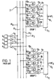
- Figure 1 illustrates a redundancy implementation circuit according to the prior art.
- Figure 1 illustrates a plurality of address pads A0,A1,A2,A3 for receiving address bits.
- the address pads A0...A3 are each connected to a line driver 4 0 ...4 3 for driving the address bits onto redundant address lines via an address bus 31.
- Two groups of redundant address lines are shown in Figure 1, GROUP0,GROUP1. They are denoted RAL 00 ,RAL 01 etc. in GROUP0 and RAL 10 ,RAL 11 etc. in GROUP1. It can be seen that redundant address lines RAL 00 ,RAL 10 share a common address line AL0 connected to pad A0 and that this also occurs for other pairs of redundant address lines in the groups.
- the redundant address lines are connected to respective comparators, 8a,8b,8c,8d, four of which are shown in Figure 1 in each group. It will be appreciated that there may be any different number of comparators depending on the number of bits in the address.
- the comparators 8a to 8d compare the address bits on redundant address lines RAL with the outputs from a corresponding plurality of memory cells 10a,10b,10c,10d. In a flash memory, these memory cells will normally be UPROM cells. Each UPROM cell 10a to 10d has an output line 12a to 12d respectively on which the bit stored in that memory cell is output for comparison at the comparator 8a to 8d.
- the outputs of the comparators 8a to 8d in each group are fed to respective compare circuits 14 0 ,14 1 which generate a hit signal HIT0,HIT1 when all of the bits stored in the memory elements 10a to 10d match the incoming bits of the redundant address.
- the hit signals are supplied on line 16 0 ,16 1 to decoding logic to access a spare element in a memory array rather than a defective element when the incoming address is the address of a defective element.
- the present invention seeks to provide a redundancy implementation circuit which can readily be tested but which minimises the number of connections which need to be routed in layout, in order to minimise the chip area.
- a redundancy implementation circuit comprising: a memory cell storing an address bit of an address identifying a redundant memory location; a comparator circuit connected to compare the address bit stored in the memory cell with an incoming address bit supplied on a redundant address line; a switch for selectively connecting the output of the memory cell to said redundant address line during a test mode; a redundant address line driver activated for supplying an incoming address bit onto said redundant address line in a normal mode; and a test line output driver connectable to said redundant address line in a test mode for driving signals on said redundant address line onto a test path when said redundant address line drivers are not activated.
- the test path may be a test bus or any other suitable test path.
- the provision of the switch allows the redundant address line to perform a dual function of supplying address bits or outputting stored bits for test, so that the chip area consumed is reduced, while nevertheless allowing the output of each memory cell to be tested individually.
- the concept of the invention can also be extended to include memory cells which do not store redundant address bits but which nevertheless store bits which are required to be tested.
- the output of these memory cells can be connected through appropriate switches to the redundant address lines in the same manner as the outputs of memory cells containing redundant address bits.
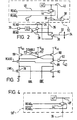
- Figure 2 illustrates the case for one address pad and one address line, for example A 0 ,AL 0 in Figure 1. It will readily be understood that the circuitry is repeated for each address pad.
- the address pad 20 for receiving address bits is connected to an address buffer 22 the output of which is connected to the redundant address line driver 24 (equivalent for example to 4 0 in Figure 1).
- the redundant address line driver 24 is controlled by complementary READ and READ signals on lines 26 and 28 respectively which are set in normal operation of the chips so that the redundant address line driver 24 is on.
- the READ and READ signals on lines 26 and 28 are also supplied to an output test line driver 30 but with reverse semantics so that when the redundant address line driver 24 is on, the output test line driver 30 is off and vice versa. It will be appreciated that there is a test line driver associated with each address line driver 4 0 ...4 3 .
- the output test line driver 30 supplies its signals on line 32 to a test IO bus 34 which is connected to an output pad (not shown) in a test mode for supplying signals off chip.
- the redundant address line driver 24 drives the incoming address bit via address line 35 and redundant address line 36 to the input of a comparator 38 (for example equivalent to 8a in Figure 1).
- Address line 35 is equivalent for example to AL 0 in Figure 1.
- Redundant address line 36 is equivalent for example to RAL 00 or RAL 10 in Figure 1.
- the comparator 38 receives another input on line 40 from a memory cell 42 (equivalent to memory cell 10a in Figure 1).
- the memory cell 42 could be a UPROM cell storing a redundant address bit and having the form shown in Figure 3.
- the UPROM cell shown in Figure 3 comprises first and second floating gate transistors 78,80. The sources of the transistors 78,80 are both connected to ground.
- the gates of the transistors are connected to a UPROM wordline UWL, which is capable of selectively connecting the gates of the floating gate transistor cells 78,80 to appropriate voltages for programming.
- the drains of the transistors are connected to bit lines UBL, UBL for the cell.
- the drains of the flash transistors 78,80 are connected through switch transistors 84,86 to a pair of p-channel cross-coupled transistors 88,90 which cooperate to remove DC current in a known manner when the cell is programmed. These cross-coupled transistors are connected in turn to a power supply voltage Vcc.
- the output 40 of the UPROM cell is taken between the transistor 90 and a switchable transistor 86 via an inverter 92.
- the gates of the switch transistors 84,86 receive an RCASC signal for activating the cell.
- RCASC is low to isolate the p-channel transistors 88,90 and transistor 82 drives the p-channel to a known state in response to a disable signal on line 112.
- the output of the memory cell 42 on line 40 is also supplied to a switch in the form of a pass gate 44 which is controlled by READ 0 and READ 0 signals on lines 46 and 48 respectively.
- a switch 44 associated with each memory cell in each group.
- the switches in GROUP0 are all controlled by READ0,READ0 signals.
- the switches in GROUP1 are all controlled by different read signals READ1, READ1 to ensure that the shared address lines are not connected simultaneously to different redundant address lines (e.g. RAL0 0 ,RAL 10 in the case of AL0).
- circuitry including the memory cell 42, pass gate 44 and its control lines 46,48 and comparator 38 is shown inside a dotted line 50. It will readily be understood that the circuitry denoted by the dotted line 50 replaces the UPROM cells 10a...10d and comparators 8a...8d shown in the prior art circuit of Figure 1. Redundant addresses are stored in the memory cells 42 and the outputs of the comparators 38 are fed in a normal mode of operation to compare circuits to generate hit signals, as discussed above with reference to the prior art. No further discussion of the precise manner of redundancy implementation is given herein because it is well known to a person skilled in the art. It will readily be apparent however that the circuit of Figure 2 differs from the circuit of Figure 1 in the provision of a switch 44 associated with each memory cell 42 and in the provision of an output test line driver 30 associated with each address line driver and connected to the shared address line 35.
- the READ and READ signals on line 26 and 28 are set so that the redundant address line drivers 24 are on. Address bits are supplied via the address pads 20 and address buffers 22 to the comparators 38 and are compared with the outputs of the memory cells 42. When the input addresses match the redundant addresses stored in the memory cells 42, hit signals are generated by the compare circuits.
- the invention provides for a special test mode.
- the READ and READ signals change state so that the redundant address line drivers 24 are off and the output test line drivers 30 are on.
- the output of a selected memory cell 42 can be connected to the redundant address line 36 through the pass gate 44 which is controlled by its control lines 46,48.
- the signals READ 0 and READ 0 would be set appropriately.
- each switch 44 is controlled by its control lines 46,48 to selectively supply outputs from the memory cells onto the shared address line 35. These signals are then supplied to the test IO bus 34 via the output test line driver 30. This allows the output of each memory cell 42 to be individually tested without the need for extra routing lines on chip.
- the invention thus allows the redundant address lines to be shared for outputting test data in a test mode onto the test IO bus.
- the principle of the invention can also be applied where the memory cells 42 are not holding redundancy address information but are holding other bits for controlling operation of the memory device and which are required to be tested.
- the output 40 of the memory cell 42 is not supplied to a comparator such as 38 but is supplied directly to another part of the integrated circuit device.
- Figure 4 shows a modified block 501 where this is the case.
- Like parts are denoted by like numerals as in Figure 2, but primed.
- the output 40' is similarly connected to the redundant address line 36 for test purposes through the pass gate 44'.
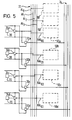
- Figure 5 is a fuller schematic of the preferred embodiment of the invention implemented for GROUP0 shown in Figure 1. Like numerals denote like parts as in Figure 2, with suffixes a...d corresponding to those in Figure 1.
- blocks 50a...50d for implementing redundancy connected respectively to address lines AL 0 ...AL 3 via redundant address lines RAL 00 ...RAL 03
- two modified blocks 50' are shown in Figure 5 connected to address lines AL 0 and AL 1 respectively.
- these modified blocks 50' may have their pass gates 44' selected to place the outputs of the memory cells within the modified blocks 50' onto address lines AL 0 and AL 1 for outputting through test output drivers 30a and 30b respectively onto the test bus 34.
- Each address line driver drives the address line on the address bus and each test output driver drives one test line on the test bus.
- the present invention can be used not only to test chips before use but also to analyse chip failures of returned chips. It can also be used in later tests to establish what data has been programmed into the UPROM cells.
Landscapes
- For Increasing The Reliability Of Semiconductor Memories (AREA)
- Tests Of Electronic Circuits (AREA)
- Read Only Memory (AREA)
- Techniques For Improving Reliability Of Storages (AREA)
Claims (9)
- Circuit de réalisation de redondance comprenant :caractérisé par un commutateur (44) pour connecter de façon sélective la sortie (40) de la cellule de mémoire à ladite ligne d'adresse redondante durant un mode de test ; etune cellule de mémoire (42) mémorisant un bit d'adresse d'une adresse identifiant un emplacement de mémoire redondante ;un circuit comparateur (38) connecté pour comparer le bit d'adresse mémorisé dans la cellule de mémoire avec un bit d'adresse entrant produit sur une ligne d'adresse redondante (34) ;un attaqueur de ligne d'adresse redondante (24) activé pour produire un bit d'adresse entrant sur ladite ligne d'adresse redondante dans un mode normal ;un attaqueur de sortie de ligne de test (30) pouvant être connecté à ladite ligne d'adresse redondante dans un mode de test pour amener des signaux sur ladite ligne d'adresse redondante sur un chemin de test lorsque lesdits attaqueurs de lignes d'adresses redondantes ne sont pas activés.
- Circuit de réalisation de redondance selon la revendication 1, comprenant une pluralité de lignes d'adresses redondantes connectées à des lignes d'adresses respectives d'un bus d'adresse, le circuit comprenant en outre une pluralité d'attaqueurs de lignes d'adresses redondantes (24a) et d'attaqueurs de sortie de ligne de test (30a) associés respectivement aux lignes d'adresses, les attaqueurs de lignes d'adresses redondantes étant connectés pour amener des bits d'adresse entrants sur lesdites lignes d'adresses redondantes.
- Circuit de réalisation de redondance selon la revendication 2, comprenant une pluralité desdites cellules de mémoire, chaque cellule de mémoire ayant ledit comparateur respectif (38) et ledit commutateur respectif (44) qui lui sont associés, dans lequel ladite pluralité de cellules de mémoire et les circuits comparateurs et commutateurs correspondants sont disposés dans un premier groupe, les sorties desdits circuits comparateurs étant fournies à un circuit de production de correspondance qui produit un signal de correspondance lorsque les bits d'adresse entrants correspondent à une adresse identifiant un premier emplacement de mémoire redondante.
- Circuit de réalisation de redondance selon la revendication 3, comprenant au moins une autre pluralité de cellules de mémoire et des circuits comparateurs et des commutateurs correspondants constituant au moins un autre groupe, les sorties des circuits comparateurs dans ledit au moins un autre groupe étant fournies à un autre circuit de production de correspondance pour produire un signal de correspondance lorsque des bits d'adresse entrants correspondent à une adresse identifiant un autre emplacement de mémoire redondante.
- Circuit de réalisation de redondance selon la revendication 4, dans lequel chaque ligne d'adresse est connectée à une ligne d'adresse redondante de chaque groupe parmi le premier groupe et le au moins un autre groupe, dans lequel le circuit de réalisation de redondance comprend en outre un circuit pour commander lesdits commutateurs dans chaque groupe de sorte que les sorties des cellules de mémoire dans un seul desdits groupes sont connectées aux lignes d'adresses à un moment donné.
- Circuit de réalisation de redondance selon la revendication 3, comprenant une autre pluralité de cellules de mémoire mémorisant chacune des bits supplémentaires respectifs ;une autre pluralité correspondante de commutateurs pour connecter de façon sélective les sorties desdites autres cellules de mémoire auxdites lignes d'adresses durant ledit mode de test.
- Circuit de réalisation de redondance selon l'une quelconque des revendications précédentes réalisé sur une puce de mémoire flash, dans lequel lesdites cellules de mémoire sont des cellules de mémoire morte non effaçable ou, en abrégé, UPROM.
- Circuit de réalisation de redondance selon la revendication 1, dans lequel l'attaqueur de ligne d'adresse redondante est connecté pour recevoir des signaux de commande complémentaires (READ,
READ ) pour mettre celui-ci sous tension et hors tension et dans lequel ledit attaqueur de sortie de ligne de test est connecté pour recevoir lesdits signaux de commande complémentaires mais dans un sens inverse, de sorte que lorsque ledit attaqueur de ligne d'adresse redondante (24) est sous tension, l'attaqueur de sortie de ligne de test (30) est hors tension, et vice versa. - Circuit de réalisation de redondance selon la revendication 3, dans lequel les attaqueurs de lignes d'adresses redondantes sont connectés pour recevoir des signaux de commande complémentaires pour les mettre sous tension et hors tension et dans lequel lesdits attaqueurs de sortie de ligne de test sont connectés pour recevoir lesdits signaux de commande complémentaires mais dans un sens inverse, de sorte que lorsque lesdits attaqueurs de lignes d'adresses redondantes sont sous tension, les attaqueurs de sortie de ligne de test sont hors tension, et vice versa.
Applications Claiming Priority (2)
| Application Number | Priority Date | Filing Date | Title |
|---|---|---|---|
| GB9417269A GB9417269D0 (en) | 1994-08-26 | 1994-08-26 | Memory and test method therefor |
| GB9417269 | 1994-08-26 |
Publications (2)
| Publication Number | Publication Date |
|---|---|
| EP0702373A1 EP0702373A1 (fr) | 1996-03-20 |
| EP0702373B1 true EP0702373B1 (fr) | 1999-12-01 |
Family
ID=10760452
Family Applications (1)
| Application Number | Title | Priority Date | Filing Date |
|---|---|---|---|
| EP95305820A Expired - Lifetime EP0702373B1 (fr) | 1994-08-26 | 1995-08-21 | Mémoire d'adresse redondante et sa méthode de test |
Country Status (5)
| Country | Link |
|---|---|
| US (1) | US5757814A (fr) |
| EP (1) | EP0702373B1 (fr) |
| JP (1) | JP2755926B2 (fr) |
| DE (1) | DE69513599T2 (fr) |
| GB (1) | GB9417269D0 (fr) |
Families Citing this family (9)
| Publication number | Priority date | Publication date | Assignee | Title |
|---|---|---|---|---|
| DE69630210D1 (de) * | 1996-06-06 | 2003-11-06 | St Microelectronics Srl | Halbleiterspeicheranordnung mit Zeilen- und Spaltenredundanzschaltungen und eine zeitverteilte Redundanzschaltungtestarchitektur |
| US5867504A (en) * | 1997-06-05 | 1999-02-02 | Sgs-Thomson Microelectronics, S.R.L. | Semiconductor memory device with row and column redundancy circuits and a time-shared redundancy circuit test architecture. |
| US7061821B2 (en) * | 1998-10-20 | 2006-06-13 | International Business Machines Corporation | Address wrap function for addressable memory devices |
| US6536003B1 (en) | 2000-02-08 | 2003-03-18 | Infineon Technologies Ag | Testable read-only memory for data memory redundant logic |
| DE10005618A1 (de) * | 2000-02-09 | 2001-08-30 | Infineon Technologies Ag | Integrierter Halbleiterspeicher mit redundanter Einheit von Speicherzellen |
| US7065683B1 (en) | 2001-12-05 | 2006-06-20 | Lsi Logic Corporation | Long path at-speed testing |
| DE10256487B4 (de) * | 2002-12-03 | 2008-12-24 | Infineon Technologies Ag | Integrierter Speicher und Verfahren zum Testen eines integrierten Speichers |
| US7131039B2 (en) * | 2002-12-11 | 2006-10-31 | Hewlett-Packard Development Company, L.P. | Repair techniques for memory with multiple redundancy |
| DE10334520B4 (de) * | 2003-07-29 | 2008-08-21 | Infineon Technologies Ag | Verfahren und Vorrichtung zur Fehlerkorrektur bei einem digitalen Speicher |
Family Cites Families (27)
| Publication number | Priority date | Publication date | Assignee | Title |
|---|---|---|---|---|
| US5046046A (en) * | 1978-03-10 | 1991-09-03 | Intel Corporation | Redundancy CAM using word line from memory |
| JPS61120399A (ja) * | 1984-11-14 | 1986-06-07 | Fujitsu Ltd | 半導体記憶装置 |
| US4796233A (en) * | 1984-10-19 | 1989-01-03 | Fujitsu Limited | Bipolar-transistor type semiconductor memory device having redundancy configuration |
| JPS61120400A (ja) * | 1984-11-14 | 1986-06-07 | Fujitsu Ltd | 半導体記憶装置 |
| JPS6214399A (ja) * | 1985-07-12 | 1987-01-22 | Fujitsu Ltd | 半導体記憶装置 |
| JPS62222500A (ja) * | 1986-03-20 | 1987-09-30 | Fujitsu Ltd | 半導体記憶装置 |
| US5617365A (en) * | 1988-10-07 | 1997-04-01 | Hitachi, Ltd. | Semiconductor device having redundancy circuit |
| JPH0359895A (ja) * | 1989-07-27 | 1991-03-14 | Nec Corp | 半導体メモリ |
| JPH03276498A (ja) * | 1990-03-27 | 1991-12-06 | Fujitsu Ltd | 半導体集積回路装置 |
| JPH0426999A (ja) * | 1990-05-19 | 1992-01-30 | Fujitsu Ltd | 冗長情報読み出し回路 |
| DE4028819A1 (de) * | 1990-09-11 | 1992-03-12 | Siemens Ag | Schaltungsanordnung zum testen eines halbleiterspeichers mittels paralleltests mit verschiedenen testbitmustern |
| FR2684206B1 (fr) * | 1991-11-25 | 1994-01-07 | Sgs Thomson Microelectronics Sa | Circuit de lecture de fusible de redondance pour memoire integree. |
| JPH05243386A (ja) * | 1992-02-27 | 1993-09-21 | Mitsubishi Electric Corp | 半導体記憶装置 |
| EP0567707A1 (fr) * | 1992-04-30 | 1993-11-03 | International Business Machines Corporation | Réalisation de redondance de colonne dans une architecture d'antémémoire |
| US5550394A (en) * | 1993-06-18 | 1996-08-27 | Texas Instruments Incorporated | Semiconductor memory device and defective memory cell correction circuit |
| US5434208A (en) * | 1992-07-10 | 1995-07-18 | Akzo Nobel N.V. | Optically non-linear active waveguiding material comprising a dopant having multiple donor-n-acceptor systems |
| DE4223532A1 (de) * | 1992-07-17 | 1994-01-20 | Philips Patentverwaltung | Schaltungsanordnung zum Prüfen der Adressierung wenigstens einer Matrix |
| FR2695493B1 (fr) * | 1992-09-08 | 1994-10-07 | Thomson Composants Militaires | Circuit de mémoire avec redondance. |
| JP2870320B2 (ja) * | 1992-09-29 | 1999-03-17 | 日本電気株式会社 | 半導体メモリ回路 |
| JPH06275095A (ja) * | 1993-03-18 | 1994-09-30 | Fujitsu Ltd | 半導体記憶装置及び冗長アドレス書込方法 |
| JP3257860B2 (ja) * | 1993-05-17 | 2002-02-18 | 株式会社日立製作所 | 半導体メモリ装置 |
| JPH07111100A (ja) * | 1993-10-08 | 1995-04-25 | Nec Corp | テスト回路 |
| EP0657814B1 (fr) * | 1993-12-07 | 1999-03-17 | STMicroelectronics S.r.l. | Circuit redondant pour une mémoire à semi-conducteurs |
| JP3215566B2 (ja) * | 1994-01-31 | 2001-10-09 | 富士通株式会社 | 半導体記憶装置 |
| EP0668563B1 (fr) * | 1994-02-17 | 1998-07-08 | STMicroelectronics S.r.l. | Procédé de programmation de registres de redondance dans un circuit intégré à redondance de rangée pour dispositif de mémoire à semi-conducteur |
| JP3530574B2 (ja) * | 1994-05-20 | 2004-05-24 | 株式会社ルネサステクノロジ | 半導体記憶装置 |
| GB9417266D0 (en) * | 1994-08-26 | 1994-10-19 | Inmos Ltd | Testing a non-volatile memory |
-
1994
- 1994-08-26 GB GB9417269A patent/GB9417269D0/en active Pending
-
1995
- 1995-08-21 DE DE69513599T patent/DE69513599T2/de not_active Expired - Fee Related
- 1995-08-21 EP EP95305820A patent/EP0702373B1/fr not_active Expired - Lifetime
- 1995-08-23 JP JP21449395A patent/JP2755926B2/ja not_active Expired - Fee Related
- 1995-08-24 US US08/519,406 patent/US5757814A/en not_active Expired - Lifetime
Also Published As
| Publication number | Publication date |
|---|---|
| DE69513599D1 (de) | 2000-01-05 |
| DE69513599T2 (de) | 2000-04-27 |
| JP2755926B2 (ja) | 1998-05-25 |
| GB9417269D0 (en) | 1994-10-19 |
| EP0702373A1 (fr) | 1996-03-20 |
| JPH0887900A (ja) | 1996-04-02 |
| US5757814A (en) | 1998-05-26 |
Similar Documents
| Publication | Publication Date | Title |
|---|---|---|
| JP3773961B2 (ja) | メモリを有する集積回路及びその動作方法 | |
| JP3129440B2 (ja) | 冗長装置を有する集積半導体メモリ | |
| US4281398A (en) | Block redundancy for memory array | |
| US5761138A (en) | Memory devices having a flexible redundant block architecture | |
| US5161157A (en) | Field-programmable redundancy apparatus for memory arrays | |
| EP0637036B1 (fr) | Vérification d'éléments de redondance dans une mémoire à circuit intégré sans programmation d'éléments de substitution redondants | |
| US5485424A (en) | Semiconductor memory and redundant-address writing method | |
| EP0657811B1 (fr) | Circuit intégré de contrÔle de l'utilisation des éléments de mémoire redondantes dans un dispositif de mémoire à semi-conducteurs | |
| US5574688A (en) | Apparatus and method for mapping a redundant memory column to a defective memory column | |
| US5659509A (en) | Method for programming redundancy registers in a row redundancy integrated circuitry for a semiconductor memory device, and row redundancy integrated circuitry | |
| US20030237033A1 (en) | System for testing a group of functionally independent memories and for replacing failing memory words | |
| JPH04139700A (ja) | 半導体記憶装置 | |
| KR20020071845A (ko) | 메모리 장치내의 멀티플렉스된 중복 계획을 위한 회로 및방법 | |
| EP0881571B1 (fr) | Dispositif de mémoire à semiconducteur avec rédondance | |
| EP0702373B1 (fr) | Mémoire d'adresse redondante et sa méthode de test | |
| KR100253687B1 (ko) | 반도체 메모리 | |
| US6058052A (en) | Redundancy scheme providing improvements in redundant circuit access time and integrated circuit layout area | |
| US6868021B2 (en) | Rapidly testable semiconductor memory device | |
| KR100281284B1 (ko) | 컬럼 리던던시 회로 | |
| KR20010014986A (ko) | 반도체 기억 장치 및 번인 테스트 방법 | |
| US5708601A (en) | Integrated circuitry for checking the utilization rate of redundancy memory elements in a semiconductor memory device | |
| US5831915A (en) | Memory device with clocked column redundancy | |
| EP0844619B1 (fr) | Mémoire non-volatile à semi-conducteur comportant un circuit de test pour tester la fonction d'éffaçage | |
| US20020060935A1 (en) | Defective address storage scheme for memory device | |
| EP0811918B1 (fr) | Dispositif de mémoire à semi-conducteur avec redondance de colonne cadencé et transfert de données de redondance à temps partagé |
Legal Events
| Date | Code | Title | Description |
|---|---|---|---|
| PUAI | Public reference made under article 153(3) epc to a published international application that has entered the european phase |
Free format text: ORIGINAL CODE: 0009012 |
|
| AK | Designated contracting states |
Kind code of ref document: A1 Designated state(s): DE FR GB IT |
|
| 17P | Request for examination filed |
Effective date: 19960323 |
|
| GRAG | Despatch of communication of intention to grant |
Free format text: ORIGINAL CODE: EPIDOS AGRA |
|
| RAP3 | Party data changed (applicant data changed or rights of an application transferred) |
Owner name: STMICROELECTRONICS LIMITED |
|
| 17Q | First examination report despatched |
Effective date: 19990216 |
|
| GRAG | Despatch of communication of intention to grant |
Free format text: ORIGINAL CODE: EPIDOS AGRA |
|
| GRAH | Despatch of communication of intention to grant a patent |
Free format text: ORIGINAL CODE: EPIDOS IGRA |
|
| GRAH | Despatch of communication of intention to grant a patent |
Free format text: ORIGINAL CODE: EPIDOS IGRA |
|
| GRAA | (expected) grant |
Free format text: ORIGINAL CODE: 0009210 |
|
| ITF | It: translation for a ep patent filed | ||
| AK | Designated contracting states |
Kind code of ref document: B1 Designated state(s): DE FR GB IT |
|
| ET | Fr: translation filed | ||
| REF | Corresponds to: |
Ref document number: 69513599 Country of ref document: DE Date of ref document: 20000105 |
|
| PLBE | No opposition filed within time limit |
Free format text: ORIGINAL CODE: 0009261 |
|
| STAA | Information on the status of an ep patent application or granted ep patent |
Free format text: STATUS: NO OPPOSITION FILED WITHIN TIME LIMIT |
|
| 26N | No opposition filed | ||
| REG | Reference to a national code |
Ref country code: GB Ref legal event code: IF02 |
|
| PGFP | Annual fee paid to national office [announced via postgrant information from national office to epo] |
Ref country code: DE Payment date: 20040902 Year of fee payment: 10 |
|
| PGFP | Annual fee paid to national office [announced via postgrant information from national office to epo] |
Ref country code: FR Payment date: 20050809 Year of fee payment: 11 |
|
| PGFP | Annual fee paid to national office [announced via postgrant information from national office to epo] |
Ref country code: GB Payment date: 20050817 Year of fee payment: 11 |
|
| PG25 | Lapsed in a contracting state [announced via postgrant information from national office to epo] |
Ref country code: IT Free format text: LAPSE BECAUSE OF NON-PAYMENT OF DUE FEES Effective date: 20050821 |
|
| PG25 | Lapsed in a contracting state [announced via postgrant information from national office to epo] |
Ref country code: DE Free format text: LAPSE BECAUSE OF NON-PAYMENT OF DUE FEES Effective date: 20060301 |
|
| GBPC | Gb: european patent ceased through non-payment of renewal fee |
Effective date: 20060821 |
|
| REG | Reference to a national code |
Ref country code: FR Ref legal event code: ST Effective date: 20070430 |
|
| PG25 | Lapsed in a contracting state [announced via postgrant information from national office to epo] |
Ref country code: GB Free format text: LAPSE BECAUSE OF NON-PAYMENT OF DUE FEES Effective date: 20060821 |
|
| PG25 | Lapsed in a contracting state [announced via postgrant information from national office to epo] |
Ref country code: FR Free format text: LAPSE BECAUSE OF NON-PAYMENT OF DUE FEES Effective date: 20060831 |