EP0702404B1 - Halbleiteranordnung vom Filmträgertyp mit Anschlusshöcher - Google Patents
Halbleiteranordnung vom Filmträgertyp mit Anschlusshöcher Download PDFInfo
- Publication number
- EP0702404B1 EP0702404B1 EP95306473A EP95306473A EP0702404B1 EP 0702404 B1 EP0702404 B1 EP 0702404B1 EP 95306473 A EP95306473 A EP 95306473A EP 95306473 A EP95306473 A EP 95306473A EP 0702404 B1 EP0702404 B1 EP 0702404B1
- Authority
- EP
- European Patent Office
- Prior art keywords
- semiconductor device
- bump
- solder
- land
- hole
- Prior art date
- Legal status (The legal status is an assumption and is not a legal conclusion. Google has not performed a legal analysis and makes no representation as to the accuracy of the status listed.)
- Expired - Lifetime
Links
Images




Classifications
-
- H—ELECTRICITY
- H05—ELECTRIC TECHNIQUES NOT OTHERWISE PROVIDED FOR
- H05K—PRINTED CIRCUITS; CASINGS OR CONSTRUCTIONAL DETAILS OF ELECTRIC APPARATUS; MANUFACTURE OF ASSEMBLAGES OF ELECTRICAL COMPONENTS
- H05K3/00—Apparatus or processes for manufacturing printed circuits
- H05K3/36—Assembling printed circuits with other printed circuits
- H05K3/361—Assembling flexible printed circuits with other printed circuits
- H05K3/363—Assembling flexible printed circuits with other printed circuits by soldering
-
- H—ELECTRICITY
- H10—SEMICONDUCTOR DEVICES; ELECTRIC SOLID-STATE DEVICES NOT OTHERWISE PROVIDED FOR
- H10W—GENERIC PACKAGES, INTERCONNECTIONS, CONNECTORS OR OTHER CONSTRUCTIONAL DETAILS OF DEVICES COVERED BY CLASS H10
- H10W70/00—Package substrates; Interposers; Redistribution layers [RDL]
- H10W70/40—Leadframes
- H10W70/453—Leadframes comprising flexible metallic tapes
-
- H—ELECTRICITY
- H10—SEMICONDUCTOR DEVICES; ELECTRIC SOLID-STATE DEVICES NOT OTHERWISE PROVIDED FOR
- H10W—GENERIC PACKAGES, INTERCONNECTIONS, CONNECTORS OR OTHER CONSTRUCTIONAL DETAILS OF DEVICES COVERED BY CLASS H10
- H10W70/00—Package substrates; Interposers; Redistribution layers [RDL]
- H10W70/60—Insulating or insulated package substrates; Interposers; Redistribution layers
- H10W70/62—Insulating or insulated package substrates; Interposers; Redistribution layers characterised by their interconnections
- H10W70/63—Vias, e.g. via plugs
- H10W70/635—Through-vias
-
- H—ELECTRICITY
- H10—SEMICONDUCTOR DEVICES; ELECTRIC SOLID-STATE DEVICES NOT OTHERWISE PROVIDED FOR
- H10W—GENERIC PACKAGES, INTERCONNECTIONS, CONNECTORS OR OTHER CONSTRUCTIONAL DETAILS OF DEVICES COVERED BY CLASS H10
- H10W74/00—Encapsulations, e.g. protective coatings
- H10W74/10—Encapsulations, e.g. protective coatings characterised by their shape or disposition
- H10W74/111—Encapsulations, e.g. protective coatings characterised by their shape or disposition the semiconductor body being completely enclosed
-
- H—ELECTRICITY
- H10—SEMICONDUCTOR DEVICES; ELECTRIC SOLID-STATE DEVICES NOT OTHERWISE PROVIDED FOR
- H10W—GENERIC PACKAGES, INTERCONNECTIONS, CONNECTORS OR OTHER CONSTRUCTIONAL DETAILS OF DEVICES COVERED BY CLASS H10
- H10W90/00—Package configurations
- H10W90/701—Package configurations characterised by the relative positions of pads or connectors relative to package parts
-
- H—ELECTRICITY
- H05—ELECTRIC TECHNIQUES NOT OTHERWISE PROVIDED FOR
- H05K—PRINTED CIRCUITS; CASINGS OR CONSTRUCTIONAL DETAILS OF ELECTRIC APPARATUS; MANUFACTURE OF ASSEMBLAGES OF ELECTRICAL COMPONENTS
- H05K1/00—Printed circuits
- H05K1/02—Details
- H05K1/0266—Marks, test patterns or identification means
- H05K1/0269—Marks, test patterns or identification means for visual or optical inspection
-
- H—ELECTRICITY
- H05—ELECTRIC TECHNIQUES NOT OTHERWISE PROVIDED FOR
- H05K—PRINTED CIRCUITS; CASINGS OR CONSTRUCTIONAL DETAILS OF ELECTRIC APPARATUS; MANUFACTURE OF ASSEMBLAGES OF ELECTRICAL COMPONENTS
- H05K2201/00—Indexing scheme relating to printed circuits covered by H05K1/00
- H05K2201/03—Conductive materials
- H05K2201/0332—Structure of the conductor
- H05K2201/0388—Other aspects of conductors
- H05K2201/0394—Conductor crossing over a hole in the substrate or a gap between two separate substrate parts
-
- H—ELECTRICITY
- H05—ELECTRIC TECHNIQUES NOT OTHERWISE PROVIDED FOR
- H05K—PRINTED CIRCUITS; CASINGS OR CONSTRUCTIONAL DETAILS OF ELECTRIC APPARATUS; MANUFACTURE OF ASSEMBLAGES OF ELECTRICAL COMPONENTS
- H05K2201/00—Indexing scheme relating to printed circuits covered by H05K1/00
- H05K2201/09—Shape and layout
- H05K2201/09209—Shape and layout details of conductors
- H05K2201/09654—Shape and layout details of conductors covering at least two types of conductors provided for in H05K2201/09218 - H05K2201/095
- H05K2201/0969—Apertured conductors
-
- H—ELECTRICITY
- H05—ELECTRIC TECHNIQUES NOT OTHERWISE PROVIDED FOR
- H05K—PRINTED CIRCUITS; CASINGS OR CONSTRUCTIONAL DETAILS OF ELECTRIC APPARATUS; MANUFACTURE OF ASSEMBLAGES OF ELECTRICAL COMPONENTS
- H05K2201/00—Indexing scheme relating to printed circuits covered by H05K1/00
- H05K2201/10—Details of components or other objects attached to or integrated in a printed circuit board
- H05K2201/10613—Details of electrical connections of non-printed components, e.g. special leads
- H05K2201/10621—Components characterised by their electrical contacts
- H05K2201/10681—Tape Carrier Package [TCP]; Flexible sheet connector
-
- H—ELECTRICITY
- H05—ELECTRIC TECHNIQUES NOT OTHERWISE PROVIDED FOR
- H05K—PRINTED CIRCUITS; CASINGS OR CONSTRUCTIONAL DETAILS OF ELECTRIC APPARATUS; MANUFACTURE OF ASSEMBLAGES OF ELECTRICAL COMPONENTS
- H05K2201/00—Indexing scheme relating to printed circuits covered by H05K1/00
- H05K2201/10—Details of components or other objects attached to or integrated in a printed circuit board
- H05K2201/10613—Details of electrical connections of non-printed components, e.g. special leads
- H05K2201/10621—Components characterised by their electrical contacts
- H05K2201/10734—Ball grid array [BGA]; Bump grid array
-
- H—ELECTRICITY
- H10—SEMICONDUCTOR DEVICES; ELECTRIC SOLID-STATE DEVICES NOT OTHERWISE PROVIDED FOR
- H10W—GENERIC PACKAGES, INTERCONNECTIONS, CONNECTORS OR OTHER CONSTRUCTIONAL DETAILS OF DEVICES COVERED BY CLASS H10
- H10W70/00—Package substrates; Interposers; Redistribution layers [RDL]
- H10W70/60—Insulating or insulated package substrates; Interposers; Redistribution layers
- H10W70/67—Insulating or insulated package substrates; Interposers; Redistribution layers characterised by their insulating layers or insulating parts
- H10W70/68—Shapes or dispositions thereof
- H10W70/682—Shapes or dispositions thereof comprising holes having chips therein
-
- H—ELECTRICITY
- H10—SEMICONDUCTOR DEVICES; ELECTRIC SOLID-STATE DEVICES NOT OTHERWISE PROVIDED FOR
- H10W—GENERIC PACKAGES, INTERCONNECTIONS, CONNECTORS OR OTHER CONSTRUCTIONAL DETAILS OF DEVICES COVERED BY CLASS H10
- H10W70/00—Package substrates; Interposers; Redistribution layers [RDL]
- H10W70/60—Insulating or insulated package substrates; Interposers; Redistribution layers
- H10W70/67—Insulating or insulated package substrates; Interposers; Redistribution layers characterised by their insulating layers or insulating parts
- H10W70/68—Shapes or dispositions thereof
- H10W70/685—Shapes or dispositions thereof comprising multiple insulating layers
-
- H—ELECTRICITY
- H10—SEMICONDUCTOR DEVICES; ELECTRIC SOLID-STATE DEVICES NOT OTHERWISE PROVIDED FOR
- H10W—GENERIC PACKAGES, INTERCONNECTIONS, CONNECTORS OR OTHER CONSTRUCTIONAL DETAILS OF DEVICES COVERED BY CLASS H10
- H10W72/00—Interconnections or connectors in packages
- H10W72/071—Connecting or disconnecting
- H10W72/072—Connecting or disconnecting of bump connectors
- H10W72/07251—Connecting or disconnecting of bump connectors characterised by changes in properties of the bump connectors during connecting
-
- H—ELECTRICITY
- H10—SEMICONDUCTOR DEVICES; ELECTRIC SOLID-STATE DEVICES NOT OTHERWISE PROVIDED FOR
- H10W—GENERIC PACKAGES, INTERCONNECTIONS, CONNECTORS OR OTHER CONSTRUCTIONAL DETAILS OF DEVICES COVERED BY CLASS H10
- H10W72/00—Interconnections or connectors in packages
- H10W72/20—Bump connectors, e.g. solder bumps or copper pillars; Dummy bumps; Thermal bumps
-
- H—ELECTRICITY
- H10—SEMICONDUCTOR DEVICES; ELECTRIC SOLID-STATE DEVICES NOT OTHERWISE PROVIDED FOR
- H10W—GENERIC PACKAGES, INTERCONNECTIONS, CONNECTORS OR OTHER CONSTRUCTIONAL DETAILS OF DEVICES COVERED BY CLASS H10
- H10W72/00—Interconnections or connectors in packages
- H10W72/701—Tape-automated bond [TAB] connectors
-
- H—ELECTRICITY
- H10—SEMICONDUCTOR DEVICES; ELECTRIC SOLID-STATE DEVICES NOT OTHERWISE PROVIDED FOR
- H10W—GENERIC PACKAGES, INTERCONNECTIONS, CONNECTORS OR OTHER CONSTRUCTIONAL DETAILS OF DEVICES COVERED BY CLASS H10
- H10W72/00—Interconnections or connectors in packages
- H10W72/851—Dispositions of multiple connectors or interconnections
- H10W72/874—On different surfaces
- H10W72/886—Die-attach connectors and strap connectors
-
- H—ELECTRICITY
- H10—SEMICONDUCTOR DEVICES; ELECTRIC SOLID-STATE DEVICES NOT OTHERWISE PROVIDED FOR
- H10W—GENERIC PACKAGES, INTERCONNECTIONS, CONNECTORS OR OTHER CONSTRUCTIONAL DETAILS OF DEVICES COVERED BY CLASS H10
- H10W74/00—Encapsulations, e.g. protective coatings
Definitions
- a plastic packaged pad array IC device is known from US-A-5 045 914 wherein a lead portion having a hole therein is exposed at a through-hole in the plastic package, allowing bumps to be formed on both sides of the device.
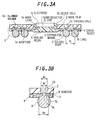
- the film carrier BGA type semiconductor device made by such process is mounted on the mounting substrate 9 by means of pads 9a and the solder bumps 6 in a package re-flowing manner.
- solder balls do not short each other since the bump pitch P2 is 1.0 mm and the diameter of the solder ball is 0.6 to 0.7 mm to which ⁇ 22 is 0.3 to 0.35 mm and the base film 2 is made of polyimide resin or the like which does not have a good wetness property to the solder.
- solder climbs up to the cover resist 4 through the aperture 3c with ⁇ 11 of 0.15 to 0.2mm formed in the center of the land 3b to form the climbed solder 6a, where the aperture 3c gives an escape for the flux and decomposed gas of the solder ball.
- the climbed bumps 6a do not short each other and the solder bumps 6 after re-flowing have an uniform profile and height of 0.4 to 0.6 mm.
Landscapes
- Engineering & Computer Science (AREA)
- Manufacturing & Machinery (AREA)
- Microelectronics & Electronic Packaging (AREA)
- Wire Bonding (AREA)
- Lead Frames For Integrated Circuits (AREA)
Claims (8)
- Halbleiterbauteil, der aufweist:gekennzeichnet durchein Filmträgerband, das einen Grundfilm (2), in dem ein Bauteilloch (2b) und ein Durchgangsloch (2a) ausgebildet sind, und eine Metallfolienverdrahtungsschicht (3) aufweist, die auf dem Grundfilm (2) ausgebildet ist, wobei die Metallfolienverdrahtungsschicht (3) ein Ende, das sich in das Bauteilloch (2b) erstreckt, um eine innere Leitung (3d) zu bilden, und ein anderes Ende aufweist, das sich auf das Durchgangsloch (2a) zu erstreckt, um einen Kontaktflecken (3b) zu bilden, der vordere und hintere Oberflächen hat;einen integrierten Halbleiterschaltungschip (1), der mit einer Elektrode (1d) versehen ist, die mit der inneren Leitung (3d) der Metallfolienverdrahtungsschicht (3) verbunden ist;wobei der Kontaktflecken (3b) im Bereich des Durchgangsloches (2a) mit einer Öffnung (3a) versehen ist, die kleiner ist als das Durchgangslochs (2a), wobei das Material des Höckers (6) durch die Öffnung (3a) hindurchgelangt und sowohl die vordere als auch die hintere Oberfläche des Kontaktfleckens (3b) berührt.einen Höcker (6) für äußere Verbindung, welcher Höcker (6) auf dem Kontaktflecken (3b) ausgebildet ist und auf der vorderen oder hinteren Oberfläche des Grundfilms (2) ausgebildet ist, welcher Höcker (6) aus einem leitenden Material hergestellt ist;
- Halbleiterbauteil nach Anspruch 1, bei dem der Kontaktflecken um die gesamte Öffnung herum frei liegt.
- Halbleiterbauteil nach Anspruch 1 oder 2, bei der Dicht-harz vorgesehen ist, um den integrierten Halbleiterschaltungschip zu schützten.
- Halbleiterbauteil nach Anspruch 1, 2 oder 3, der weiter eine Schutzabdeckung aufweist, die auf der Metallfolienverdrahtungsschicht ausgebildet ist und eine Öffnung aufweist, die dem Kontaktflecken entspricht.
- Halbleiterbauteil nach Anspruch 4, bei der die Öffnung der Schutzabdeckung Abmessungen hat, die größer sind als das Durchgangsloch.
- Halbleiterbauteil nach einem vorangehenden Anspruch, bei dem der Kontakthöcker aus einer Lötmittelkugel hergestellt ist.
- Halbleiterbauteil nach einem vorangehenden Anspruch, bei dem der innere Draht und/oder der Kontaktflecken der Metallfolienschicht mit Gold, Zinn oder ähnlichem plattiert ist.
- Halbleiterbauteil nach einem vorangehenden Anspruch, bei dem die Elektrode der integrierten Halbleiterschaltung einen Höcker bildet.
Applications Claiming Priority (3)
| Application Number | Priority Date | Filing Date | Title |
|---|---|---|---|
| JP244922/94 | 1994-09-14 | ||
| JP24492294 | 1994-09-14 | ||
| JP6244922A JP2595909B2 (ja) | 1994-09-14 | 1994-09-14 | 半導体装置 |
Publications (3)
| Publication Number | Publication Date |
|---|---|
| EP0702404A2 EP0702404A2 (de) | 1996-03-20 |
| EP0702404A3 EP0702404A3 (de) | 1997-11-05 |
| EP0702404B1 true EP0702404B1 (de) | 2002-03-06 |
Family
ID=17125976
Family Applications (1)
| Application Number | Title | Priority Date | Filing Date |
|---|---|---|---|
| EP95306473A Expired - Lifetime EP0702404B1 (de) | 1994-09-14 | 1995-09-14 | Halbleiteranordnung vom Filmträgertyp mit Anschlusshöcher |
Country Status (4)
| Country | Link |
|---|---|
| US (1) | US5668405A (de) |
| EP (1) | EP0702404B1 (de) |
| JP (1) | JP2595909B2 (de) |
| DE (1) | DE69525697T2 (de) |
Families Citing this family (140)
| Publication number | Priority date | Publication date | Assignee | Title |
|---|---|---|---|---|
| JPH08288424A (ja) * | 1995-04-18 | 1996-11-01 | Nec Corp | 半導体装置 |
| JP2899540B2 (ja) * | 1995-06-12 | 1999-06-02 | 日東電工株式会社 | フィルムキャリアおよびこれを用いた半導体装置 |
| JP2894254B2 (ja) * | 1995-09-20 | 1999-05-24 | ソニー株式会社 | 半導体パッケージの製造方法 |
| US5847455A (en) * | 1995-11-07 | 1998-12-08 | Vlsi Technology, Inc. | Molded leadframe ball grid array |
| US6861290B1 (en) | 1995-12-19 | 2005-03-01 | Micron Technology, Inc. | Flip-chip adaptor package for bare die |
| JP2891665B2 (ja) * | 1996-03-22 | 1999-05-17 | 株式会社日立製作所 | 半導体集積回路装置およびその製造方法 |
| US20040061220A1 (en) * | 1996-03-22 | 2004-04-01 | Chuichi Miyazaki | Semiconductor device and manufacturing method thereof |
| KR100216839B1 (ko) * | 1996-04-01 | 1999-09-01 | 김규현 | Bga 반도체 패키지의 솔더 볼 랜드 메탈 구조 |
| DE19719983C2 (de) * | 1996-05-17 | 2003-05-15 | Nat Semiconductor Corp | Montageplatte für Halbleiterbausteine und Verfahren zur Herstellung hiervon |
| US5783866A (en) * | 1996-05-17 | 1998-07-21 | National Semiconductor Corporation | Low cost ball grid array device and method of manufacture thereof |
| DE19758547B4 (de) * | 1996-05-17 | 2005-01-20 | National Semiconductor Corp.(N.D.Ges.D.Staates Delaware), Santa Clara | Halbleiterbaustein |
| JPH09312374A (ja) * | 1996-05-24 | 1997-12-02 | Sony Corp | 半導体パッケージ及びその製造方法 |
| US5731244A (en) | 1996-05-28 | 1998-03-24 | Micron Technology, Inc. | Laser wire bonding for wire embedded dielectrics to integrated circuits |
| US6791194B1 (en) | 1996-05-30 | 2004-09-14 | Hitachi, Ltd. | Circuit tape having adhesive film, semiconductor device, and a method for manufacturing the same |
| JP2755252B2 (ja) * | 1996-05-30 | 1998-05-20 | 日本電気株式会社 | 半導体装置用パッケージ及び半導体装置 |
| JP3195236B2 (ja) | 1996-05-30 | 2001-08-06 | 株式会社日立製作所 | 接着フィルムを有する配線テープ,半導体装置及び製造方法 |
| JP2908330B2 (ja) * | 1996-07-16 | 1999-06-21 | 九州日本電気株式会社 | リードフレーム,半導体装置及び半導体装置の製造方法 |
| US6222272B1 (en) | 1996-08-06 | 2001-04-24 | Nitto Denko Corporation | Film carrier and semiconductor device using same |
| JP2828053B2 (ja) * | 1996-08-15 | 1998-11-25 | 日本電気株式会社 | 半導体装置 |
| KR100187715B1 (ko) * | 1996-08-19 | 1999-06-01 | 윤종용 | 리드 프레임을 이용한 칩 스케일 패키지 제조 방법 |
| US5863812A (en) * | 1996-09-19 | 1999-01-26 | Vlsi Technology, Inc. | Process for manufacturing a multi layer bumped semiconductor device |
| US6093971A (en) * | 1996-10-14 | 2000-07-25 | Fraunhofer-Gesellschaft Zur Forderung Der Angewandten Forschung E.V. | Chip module with conductor paths on the chip bonding side of a chip carrier |
| KR100447313B1 (ko) | 1996-11-21 | 2004-09-07 | 가부시키가이샤 히타치세이사쿠쇼 | 반도체 장치 및 그 제조방법 |
| JP3695893B2 (ja) * | 1996-12-03 | 2005-09-14 | 沖電気工業株式会社 | 半導体装置とその製造方法および実装方法 |
| KR19980044250A (ko) * | 1996-12-06 | 1998-09-05 | 황인길 | 리드 프레임의 제조 방법 및 이를 이용한 칩 스케일 반도체 패키지 |
| JP2982729B2 (ja) * | 1997-01-16 | 1999-11-29 | 日本電気株式会社 | 半導体装置 |
| JP2924840B2 (ja) * | 1997-02-13 | 1999-07-26 | 日本電気株式会社 | Tape−BGAタイプの半導体装置 |
| US5969424A (en) * | 1997-03-19 | 1999-10-19 | Fujitsu Limited | Semiconductor device with pad structure |
| JPH10294418A (ja) * | 1997-04-21 | 1998-11-04 | Oki Electric Ind Co Ltd | 半導体装置 |
| US6057594A (en) * | 1997-04-23 | 2000-05-02 | Lsi Logic Corporation | High power dissipating tape ball grid array package |
| JP3639088B2 (ja) * | 1997-06-06 | 2005-04-13 | 株式会社ルネサステクノロジ | 半導体装置及び配線テープ |
| JPH1154658A (ja) * | 1997-07-30 | 1999-02-26 | Hitachi Ltd | 半導体装置及びその製造方法並びにフレーム構造体 |
| US6028354A (en) | 1997-10-14 | 2000-02-22 | Amkor Technology, Inc. | Microelectronic device package having a heat sink structure for increasing the thermal conductivity of the package |
| JP3655069B2 (ja) * | 1997-10-27 | 2005-06-02 | 沖電気工業株式会社 | 樹脂封止型半導体装置とその製造方法 |
| US5837558A (en) * | 1997-11-04 | 1998-11-17 | Texas Instruments Incorporated | Integrated circuit chip packaging method |
| JP3645701B2 (ja) * | 1997-12-16 | 2005-05-11 | 株式会社三井ハイテック | 半導体装置 |
| JPH11204699A (ja) * | 1998-01-09 | 1999-07-30 | Sony Corp | 半導体装置とその製造方法と電子装置 |
| JPH11214435A (ja) * | 1998-01-26 | 1999-08-06 | Sharp Corp | 半導体装置およびその製造方法 |
| US6111324A (en) * | 1998-02-05 | 2000-08-29 | Asat, Limited | Integrated carrier ring/stiffener and method for manufacturing a flexible integrated circuit package |
| JPH11312749A (ja) * | 1998-02-25 | 1999-11-09 | Fujitsu Ltd | 半導体装置及びその製造方法及びリードフレームの製造方法 |
| JP3257500B2 (ja) * | 1998-02-27 | 2002-02-18 | ティーディーケイ株式会社 | 磁気ヘッド装置 |
| USRE43112E1 (en) | 1998-05-04 | 2012-01-17 | Round Rock Research, Llc | Stackable ball grid array package |
| US6072233A (en) | 1998-05-04 | 2000-06-06 | Micron Technology, Inc. | Stackable ball grid array package |
| US6404067B1 (en) | 1998-06-01 | 2002-06-11 | Intel Corporation | Plastic ball grid array package with improved moisture resistance |
| JP3727172B2 (ja) * | 1998-06-09 | 2005-12-14 | 沖電気工業株式会社 | 半導体装置 |
| US6414391B1 (en) * | 1998-06-30 | 2002-07-02 | Micron Technology, Inc. | Module assembly for stacked BGA packages with a common bus bar in the assembly |
| US6297548B1 (en) * | 1998-06-30 | 2001-10-02 | Micron Technology, Inc. | Stackable ceramic FBGA for high thermal applications |
| US5972735A (en) * | 1998-07-14 | 1999-10-26 | National Starch And Chemical Investment Holding Corporation | Method of preparing an electronic package by co-curing adhesive and encapsulant |
| JP3420703B2 (ja) * | 1998-07-16 | 2003-06-30 | 株式会社東芝 | 半導体装置の製造方法 |
| US5910686A (en) * | 1998-07-23 | 1999-06-08 | Vlsi Technology, Inc. | Cavity down HBGA package structure |
| US6400018B2 (en) * | 1998-08-27 | 2002-06-04 | 3M Innovative Properties Company | Via plug adapter |
| US6121576A (en) | 1998-09-02 | 2000-09-19 | Micron Technology, Inc. | Method and process of contact to a heat softened solder ball array |
| JP2943805B1 (ja) * | 1998-09-17 | 1999-08-30 | 日本電気株式会社 | 半導体装置及びその製造方法 |
| US6232706B1 (en) * | 1998-11-12 | 2001-05-15 | The Board Of Trustees Of The Leland Stanford Junior University | Self-oriented bundles of carbon nanotubes and method of making same |
| JP3502776B2 (ja) * | 1998-11-26 | 2004-03-02 | 新光電気工業株式会社 | バンプ付き金属箔及び回路基板及びこれを用いた半導体装置 |
| US6455354B1 (en) | 1998-12-30 | 2002-09-24 | Micron Technology, Inc. | Method of fabricating tape attachment chip-on-board assemblies |
| DE19907168C1 (de) | 1999-02-19 | 2000-08-10 | Micronas Intermetall Gmbh | Schichtanordnung sowie Verfahren zu deren Herstellung |
| KR100960739B1 (ko) * | 1999-02-26 | 2010-06-01 | 텍사스 인스트루먼츠 인코포레이티드 | 열적으로 향상된 반도체 볼 그리드 어레이 디바이스 및 그제조 방법 |
| US6462414B1 (en) | 1999-03-05 | 2002-10-08 | Altera Corporation | Integrated circuit package utilizing a conductive structure for interlocking a conductive ball to a ball pad |
| US6023097A (en) * | 1999-03-17 | 2000-02-08 | Chipmos Technologies, Inc. | Stacked multiple-chip module micro ball grid array packaging |
| JP3844936B2 (ja) | 1999-03-26 | 2006-11-15 | 富士通株式会社 | 半導体装置 |
| JP3575001B2 (ja) | 1999-05-07 | 2004-10-06 | アムコー テクノロジー コリア インコーポレーティド | 半導体パッケージ及びその製造方法 |
| JP3398721B2 (ja) | 1999-05-20 | 2003-04-21 | アムコー テクノロジー コリア インコーポレーティド | 半導体パッケージ及びその製造方法 |
| USRE40112E1 (en) | 1999-05-20 | 2008-02-26 | Amkor Technology, Inc. | Semiconductor package and method for fabricating the same |
| JP3314304B2 (ja) | 1999-06-07 | 2002-08-12 | アムコー テクノロジー コリア インコーポレーティド | 半導体パッケージ用の回路基板 |
| JP3526788B2 (ja) * | 1999-07-01 | 2004-05-17 | 沖電気工業株式会社 | 半導体装置の製造方法 |
| JP2001077301A (ja) * | 1999-08-24 | 2001-03-23 | Amkor Technology Korea Inc | 半導体パッケージ及びその製造方法 |
| US6534861B1 (en) * | 1999-11-15 | 2003-03-18 | Substrate Technologies Incorporated | Ball grid substrate for lead-on-chip semiconductor package |
| US6468891B2 (en) * | 2000-02-24 | 2002-10-22 | Micron Technology, Inc. | Stereolithographically fabricated conductive elements, semiconductor device components and assemblies including such conductive elements, and methods |
| JP3752949B2 (ja) * | 2000-02-28 | 2006-03-08 | 日立化成工業株式会社 | 配線基板及び半導体装置 |
| JP2001339011A (ja) * | 2000-03-24 | 2001-12-07 | Shinko Electric Ind Co Ltd | 半導体装置およびその製造方法 |
| KR100332967B1 (ko) * | 2000-05-10 | 2002-04-19 | 윤종용 | 디지털 마이크로-미러 디바이스 패키지의 제조 방법 |
| US6522018B1 (en) | 2000-05-16 | 2003-02-18 | Micron Technology, Inc. | Ball grid array chip packages having improved testing and stacking characteristics |
| JP3442721B2 (ja) | 2000-05-24 | 2003-09-02 | 沖電気工業株式会社 | 半導体装置 |
| US6388199B1 (en) * | 2000-07-31 | 2002-05-14 | Micron Technology, Inc. | Selectively adjusting surface tension of soldermask material |
| US7094676B1 (en) | 2000-10-13 | 2006-08-22 | Bridge Semiconductor Corporation | Semiconductor chip assembly with embedded metal pillar |
| US7190080B1 (en) * | 2000-10-13 | 2007-03-13 | Bridge Semiconductor Corporation | Semiconductor chip assembly with embedded metal pillar |
| US6552436B2 (en) * | 2000-12-08 | 2003-04-22 | Motorola, Inc. | Semiconductor device having a ball grid array and method therefor |
| US6564454B1 (en) | 2000-12-28 | 2003-05-20 | Amkor Technology, Inc. | Method of making and stacking a semiconductor package |
| US6448506B1 (en) | 2000-12-28 | 2002-09-10 | Amkor Technology, Inc. | Semiconductor package and circuit board for making the package |
| US7034386B2 (en) * | 2001-03-26 | 2006-04-25 | Nec Corporation | Thin planar semiconductor device having electrodes on both surfaces and method of fabricating same |
| US7115986B2 (en) * | 2001-05-02 | 2006-10-03 | Micron Technology, Inc. | Flexible ball grid array chip scale packages |
| US6664618B2 (en) * | 2001-05-16 | 2003-12-16 | Oki Electric Industry Co., Ltd. | Tape carrier package having stacked semiconductor elements, and short and long leads |
| DE10126655A1 (de) | 2001-06-01 | 2002-12-05 | Endress & Hauser Gmbh & Co Kg | Leiterplatte mit mindestens einem elektronischen Bauteil |
| US6730536B1 (en) | 2001-06-28 | 2004-05-04 | Amkor Technology, Inc. | Pre-drilled image sensor package fabrication method |
| SG122743A1 (en) | 2001-08-21 | 2006-06-29 | Micron Technology Inc | Microelectronic devices and methods of manufacture |
| US7335995B2 (en) | 2001-10-09 | 2008-02-26 | Tessera, Inc. | Microelectronic assembly having array including passive elements and interconnects |
| US6977440B2 (en) | 2001-10-09 | 2005-12-20 | Tessera, Inc. | Stacked packages |
| WO2003032370A2 (en) * | 2001-10-09 | 2003-04-17 | Tessera, Inc. | Stacked packages |
| US6708871B2 (en) * | 2002-01-08 | 2004-03-23 | International Business Machines Corporation | Method for forming solder connections on a circuitized substrate |
| SG104293A1 (en) * | 2002-01-09 | 2004-06-21 | Micron Technology Inc | Elimination of rdl using tape base flip chip on flex for die stacking |
| US6732908B2 (en) * | 2002-01-18 | 2004-05-11 | International Business Machines Corporation | High density raised stud microjoining system and methods of fabricating the same |
| SG115455A1 (en) | 2002-03-04 | 2005-10-28 | Micron Technology Inc | Methods for assembly and packaging of flip chip configured dice with interposer |
| SG121707A1 (en) | 2002-03-04 | 2006-05-26 | Micron Technology Inc | Method and apparatus for flip-chip packaging providing testing capability |
| SG115459A1 (en) | 2002-03-04 | 2005-10-28 | Micron Technology Inc | Flip chip packaging using recessed interposer terminals |
| SG115456A1 (en) | 2002-03-04 | 2005-10-28 | Micron Technology Inc | Semiconductor die packages with recessed interconnecting structures and methods for assembling the same |
| US6975035B2 (en) | 2002-03-04 | 2005-12-13 | Micron Technology, Inc. | Method and apparatus for dielectric filling of flip chip on interposer assembly |
| SG111935A1 (en) | 2002-03-04 | 2005-06-29 | Micron Technology Inc | Interposer configured to reduce the profiles of semiconductor device assemblies and packages including the same and methods |
| US6765288B2 (en) * | 2002-08-05 | 2004-07-20 | Tessera, Inc. | Microelectronic adaptors, assemblies and methods |
| WO2004017399A1 (en) * | 2002-08-16 | 2004-02-26 | Tessera, Inc. | Microelectronic packages with self-aligning features |
| US20040036170A1 (en) | 2002-08-20 | 2004-02-26 | Lee Teck Kheng | Double bumping of flexible substrate for first and second level interconnects |
| US7294928B2 (en) * | 2002-09-06 | 2007-11-13 | Tessera, Inc. | Components, methods and assemblies for stacked packages |
| US7071547B2 (en) * | 2002-09-11 | 2006-07-04 | Tessera, Inc. | Assemblies having stacked semiconductor chips and methods of making same |
| CN1711636A (zh) * | 2002-10-11 | 2005-12-21 | 德塞拉股份有限公司 | 用于多芯片封装的元件、方法和组件 |
| US6936922B1 (en) | 2003-09-26 | 2005-08-30 | Amkor Technology, Inc. | Semiconductor package structure reducing warpage and manufacturing method thereof |
| US7061121B2 (en) | 2003-11-12 | 2006-06-13 | Tessera, Inc. | Stacked microelectronic assemblies with central contacts |
| US20070145548A1 (en) * | 2003-12-22 | 2007-06-28 | Amkor Technology, Inc. | Stack-type semiconductor package and manufacturing method thereof |
| US7009296B1 (en) | 2004-01-15 | 2006-03-07 | Amkor Technology, Inc. | Semiconductor package with substrate coupled to a peripheral side surface of a semiconductor die |
| DE102004009056B4 (de) * | 2004-02-23 | 2010-04-22 | Infineon Technologies Ag | Verfahren zur Herstellung eines Halbleitermoduls aus mehreren stapelbaren Halbleiterbauteilen mit einem Umverdrahtungssubstrat |
| TWI236742B (en) * | 2004-03-02 | 2005-07-21 | Kingtron Electronics Co Ltd | Manufacturing method of film carrier |
| US7205178B2 (en) * | 2004-03-24 | 2007-04-17 | Freescale Semiconductor, Inc. | Land grid array packaged device and method of forming same |
| TW200539246A (en) | 2004-05-26 | 2005-12-01 | Matsushita Electric Industrial Co Ltd | Semiconductor device and method for manufacturing the same |
| US7446399B1 (en) | 2004-08-04 | 2008-11-04 | Altera Corporation | Pad structures to improve board-level reliability of solder-on-pad BGA structures |
| JP4091938B2 (ja) | 2004-10-21 | 2008-05-28 | 日東電工株式会社 | 配線回路基板の製造方法 |
| JP5000877B2 (ja) * | 2005-10-07 | 2012-08-15 | ルネサスエレクトロニクス株式会社 | 半導体装置 |
| JP4842574B2 (ja) * | 2005-07-13 | 2011-12-21 | 三菱電機株式会社 | 半導体装置の製造方法 |
| TWI267967B (en) * | 2005-07-14 | 2006-12-01 | Chipmos Technologies Inc | Chip package without a core and stacked chip package structure using the same |
| TWI292195B (en) * | 2005-08-31 | 2008-01-01 | Semiconductor chip assembly with metal containment wall and solder terminal | |
| US7675152B2 (en) * | 2005-09-01 | 2010-03-09 | Texas Instruments Incorporated | Package-on-package semiconductor assembly |
| US8067831B2 (en) * | 2005-09-16 | 2011-11-29 | Stats Chippac Ltd. | Integrated circuit package system with planar interconnects |
| US7416923B2 (en) * | 2005-12-09 | 2008-08-26 | International Business Machines Corporation | Underfill film having thermally conductive sheet |
| JP5085932B2 (ja) | 2006-02-21 | 2012-11-28 | パナソニック株式会社 | 実装体及びその製造方法 |
| US20070216033A1 (en) | 2006-03-20 | 2007-09-20 | Corisis David J | Carrierless chip package for integrated circuit devices, and methods of making same |
| US7545029B2 (en) | 2006-08-18 | 2009-06-09 | Tessera, Inc. | Stack microelectronic assemblies |
| US9466545B1 (en) | 2007-02-21 | 2016-10-11 | Amkor Technology, Inc. | Semiconductor package in package |
| US9059074B2 (en) * | 2008-03-26 | 2015-06-16 | Stats Chippac Ltd. | Integrated circuit package system with planar interconnect |
| SG142321A1 (en) | 2008-04-24 | 2009-11-26 | Micron Technology Inc | Pre-encapsulated cavity interposer |
| FI125526B (fi) * | 2008-08-25 | 2015-11-13 | Ge Embedded Electronics Oy | Sähköisiä komponentteja sisältävä paketoitu piirilevyrakenne ja menetelmä sähköisiä komponentteja sisältävän paketoidun piirilevyrakenteen valmistamiseksi |
| US8043894B2 (en) * | 2008-08-26 | 2011-10-25 | Stats Chippac Ltd. | Integrated circuit package system with redistribution layer |
| TWI378546B (en) * | 2009-09-16 | 2012-12-01 | Powertech Technology Inc | Substrate and package for micro bga |
| US9420707B2 (en) | 2009-12-17 | 2016-08-16 | Intel Corporation | Substrate for integrated circuit devices including multi-layer glass core and methods of making the same |
| US8207453B2 (en) | 2009-12-17 | 2012-06-26 | Intel Corporation | Glass core substrate for integrated circuit devices and methods of making the same |
| US8482136B2 (en) * | 2009-12-29 | 2013-07-09 | Nxp B.V. | Fan-out chip scale package |
| KR20120063202A (ko) * | 2010-12-07 | 2012-06-15 | 삼성전자주식회사 | 반도체 패키지 및 이를 포함하는 디스플레이 패널 어셈블리 |
| WO2013133827A1 (en) | 2012-03-07 | 2013-09-12 | Intel Corporation | Glass clad microelectronic substrate |
| US9001520B2 (en) * | 2012-09-24 | 2015-04-07 | Intel Corporation | Microelectronic structures having laminated or embedded glass routing structures for high density packaging |
| US20150049443A1 (en) * | 2013-08-13 | 2015-02-19 | Infineon Technologies Ag | Chip arrangement |
| US9484278B2 (en) * | 2013-11-27 | 2016-11-01 | Infineon Technologies Ag | Semiconductor package and method for producing the same |
| US9735032B2 (en) * | 2013-12-06 | 2017-08-15 | Enablink Technologies Limited | System and method for manufacturing a fabricated carrier |
| US20240162126A1 (en) * | 2022-11-14 | 2024-05-16 | Nanya Technology Corporation | Semiconductor package and manufacturing method thereof |
Family Cites Families (7)
| Publication number | Priority date | Publication date | Assignee | Title |
|---|---|---|---|---|
| JPS6057222B2 (ja) * | 1980-03-26 | 1985-12-13 | シャープ株式会社 | フィルムキャリァ型半導体装置 |
| US5468681A (en) * | 1989-08-28 | 1995-11-21 | Lsi Logic Corporation | Process for interconnecting conductive substrates using an interposer having conductive plastic filled vias |
| US5045914A (en) * | 1989-12-26 | 1991-09-03 | Motorola, Inc. | Plastic pad array electronic AC device |
| US5045921A (en) * | 1989-12-26 | 1991-09-03 | Motorola, Inc. | Pad array carrier IC device using flexible tape |
| JPH06268101A (ja) * | 1993-03-17 | 1994-09-22 | Hitachi Ltd | 半導体装置及びその製造方法、電子装置、リ−ドフレ−ム並びに実装基板 |
| US5397921A (en) * | 1993-09-03 | 1995-03-14 | Advanced Semiconductor Assembly Technology | Tab grid array |
| TW258829B (de) * | 1994-01-28 | 1995-10-01 | Ibm |
-
1994
- 1994-09-14 JP JP6244922A patent/JP2595909B2/ja not_active Expired - Lifetime
-
1995
- 1995-09-14 EP EP95306473A patent/EP0702404B1/de not_active Expired - Lifetime
- 1995-09-14 US US08/528,244 patent/US5668405A/en not_active Expired - Fee Related
- 1995-09-14 DE DE69525697T patent/DE69525697T2/de not_active Expired - Fee Related
Also Published As
| Publication number | Publication date |
|---|---|
| JP2595909B2 (ja) | 1997-04-02 |
| EP0702404A3 (de) | 1997-11-05 |
| EP0702404A2 (de) | 1996-03-20 |
| JPH0888245A (ja) | 1996-04-02 |
| DE69525697D1 (de) | 2002-04-11 |
| US5668405A (en) | 1997-09-16 |
| DE69525697T2 (de) | 2002-11-28 |
Similar Documents
| Publication | Publication Date | Title |
|---|---|---|
| EP0702404B1 (de) | Halbleiteranordnung vom Filmträgertyp mit Anschlusshöcher | |
| KR100231276B1 (ko) | 반도체패키지의 구조 및 제조방법 | |
| US6175151B1 (en) | Film carrier tape, semiconductor assembly, semiconductor device, and method of manufacturing the same, mounted board, and electronic instrument | |
| US5841194A (en) | Chip carrier with peripheral stiffener and semiconductor device using the same | |
| US6734557B2 (en) | Semiconductor device | |
| JP2949490B2 (ja) | 半導体パッケージの製造方法 | |
| US6573609B2 (en) | Microelectronic component with rigid interposer | |
| US6414849B1 (en) | Low stress and low profile cavity down flip chip and wire bond BGA package | |
| KR20000022103A (ko) | Ni-b 도금층을 가진 c4 기판 접점 패드 | |
| JPH1116933A (ja) | 金属バンプを有する回路基板の製造方法及びこの回路基板を利用した半導体チップパッケージの製造方法 | |
| KR100244965B1 (ko) | 인쇄회로기판과 볼 그리드 어레이 패키지의 제조 방법 | |
| JP2001217341A (ja) | リードピン付き配線基板 | |
| JP3450236B2 (ja) | 半導体装置及びその製造方法 | |
| US5661337A (en) | Technique for improving bonding strength of leadframe to substrate in semiconductor IC chip packages | |
| US6989606B2 (en) | BGA substrate via structure | |
| US6222738B1 (en) | Packaging structure for a semiconductor element flip-chip mounted on a mounting board having staggered bump connection location on the pads and method thereof | |
| US7169643B1 (en) | Semiconductor device, method of fabricating the same, circuit board, and electronic apparatus | |
| JPH11163024A (ja) | 半導体装置とこれを組み立てるためのリードフレーム、及び半導体装置の製造方法 | |
| JP2000040713A (ja) | 半導体パッケージの製造方法 | |
| JP3585806B2 (ja) | ピン付き配線基板 | |
| JPH10178144A (ja) | Bga型電子部品の同軸電極構造 | |
| KR100565766B1 (ko) | 반도체 칩 패키지 및 그 제조방법 | |
| US6645794B2 (en) | Method of manufacturing a semiconductor device by monolithically forming a sealing resin for sealing a chip and a reinforcing frame by transfer molding | |
| KR20120047098A (ko) | 패키지 기판용 리드핀과 상기 리드핀을 포함하는 반도체 패키지 인쇄회로기판 및 그 제조방법. | |
| JP2001185639A (ja) | リードピン付き基板 |
Legal Events
| Date | Code | Title | Description |
|---|---|---|---|
| PUAI | Public reference made under article 153(3) epc to a published international application that has entered the european phase |
Free format text: ORIGINAL CODE: 0009012 |
|
| AK | Designated contracting states |
Kind code of ref document: A2 Designated state(s): DE FR GB IT |
|
| PUAL | Search report despatched |
Free format text: ORIGINAL CODE: 0009013 |
|
| AK | Designated contracting states |
Kind code of ref document: A3 Designated state(s): DE FR GB IT |
|
| 17P | Request for examination filed |
Effective date: 19971013 |
|
| 17Q | First examination report despatched |
Effective date: 19980924 |
|
| RTI1 | Title (correction) |
Free format text: SEMICONDUCTOR DEVICE COMPRISING A FILM CARRIER TAPE AND BUMP |
|
| GRAG | Despatch of communication of intention to grant |
Free format text: ORIGINAL CODE: EPIDOS AGRA |
|
| GRAG | Despatch of communication of intention to grant |
Free format text: ORIGINAL CODE: EPIDOS AGRA |
|
| GRAG | Despatch of communication of intention to grant |
Free format text: ORIGINAL CODE: EPIDOS AGRA |
|
| GRAH | Despatch of communication of intention to grant a patent |
Free format text: ORIGINAL CODE: EPIDOS IGRA |
|
| GRAH | Despatch of communication of intention to grant a patent |
Free format text: ORIGINAL CODE: EPIDOS IGRA |
|
| REG | Reference to a national code |
Ref country code: GB Ref legal event code: IF02 |
|
| GRAA | (expected) grant |
Free format text: ORIGINAL CODE: 0009210 |
|
| AK | Designated contracting states |
Kind code of ref document: B1 Designated state(s): DE FR GB IT |
|
| PG25 | Lapsed in a contracting state [announced via postgrant information from national office to epo] |
Ref country code: IT Free format text: LAPSE BECAUSE OF FAILURE TO SUBMIT A TRANSLATION OF THE DESCRIPTION OR TO PAY THE FEE WITHIN THE PRESCRIBED TIME-LIMIT;WARNING: LAPSES OF ITALIAN PATENTS WITH EFFECTIVE DATE BEFORE 2007 MAY HAVE OCCURRED AT ANY TIME BEFORE 2007. THE CORRECT EFFECTIVE DATE MAY BE DIFFERENT FROM THE ONE RECORDED. Effective date: 20020306 Ref country code: FR Free format text: LAPSE BECAUSE OF FAILURE TO SUBMIT A TRANSLATION OF THE DESCRIPTION OR TO PAY THE FEE WITHIN THE PRESCRIBED TIME-LIMIT Effective date: 20020306 |
|
| REF | Corresponds to: |
Ref document number: 69525697 Country of ref document: DE Date of ref document: 20020411 |
|
| PG25 | Lapsed in a contracting state [announced via postgrant information from national office to epo] |
Ref country code: GB Free format text: LAPSE BECAUSE OF NON-PAYMENT OF DUE FEES Effective date: 20020914 |
|
| EN | Fr: translation not filed | ||
| PLBE | No opposition filed within time limit |
Free format text: ORIGINAL CODE: 0009261 |
|
| STAA | Information on the status of an ep patent application or granted ep patent |
Free format text: STATUS: NO OPPOSITION FILED WITHIN TIME LIMIT |
|
| 26N | No opposition filed |
Effective date: 20021209 |
|
| PG25 | Lapsed in a contracting state [announced via postgrant information from national office to epo] |
Ref country code: DE Free format text: LAPSE BECAUSE OF NON-PAYMENT OF DUE FEES Effective date: 20030401 |
|
| GBPC | Gb: european patent ceased through non-payment of renewal fee |
Effective date: 20020914 |