EP0702507A1 - Flash tube devices - Google Patents
Flash tube devices Download PDFInfo
- Publication number
- EP0702507A1 EP0702507A1 EP95113405A EP95113405A EP0702507A1 EP 0702507 A1 EP0702507 A1 EP 0702507A1 EP 95113405 A EP95113405 A EP 95113405A EP 95113405 A EP95113405 A EP 95113405A EP 0702507 A1 EP0702507 A1 EP 0702507A1
- Authority
- EP
- European Patent Office
- Prior art keywords
- flash tube
- light
- flash
- electrical energy
- monitoring
- Prior art date
- Legal status (The legal status is an assumption and is not a legal conclusion. Google has not performed a legal analysis and makes no representation as to the accuracy of the status listed.)
- Withdrawn
Links
- 230000004044 response Effects 0.000 claims abstract description 26
- 239000003990 capacitor Substances 0.000 claims description 39
- 238000012544 monitoring process Methods 0.000 claims description 31
- 238000000034 method Methods 0.000 claims description 10
- 239000000758 substrate Substances 0.000 claims description 9
- 238000003384 imaging method Methods 0.000 claims description 4
- 238000006243 chemical reaction Methods 0.000 claims 1
- 238000010586 diagram Methods 0.000 description 10
- 230000015556 catabolic process Effects 0.000 description 8
- 238000006731 degradation reaction Methods 0.000 description 8
- 238000004804 winding Methods 0.000 description 8
- 230000007423 decrease Effects 0.000 description 4
- 230000008901 benefit Effects 0.000 description 3
- 239000000463 material Substances 0.000 description 3
- 238000012986 modification Methods 0.000 description 3
- 230000004048 modification Effects 0.000 description 3
- VYPSYNLAJGMNEJ-UHFFFAOYSA-N silicon dioxide Inorganic materials O=[Si]=O VYPSYNLAJGMNEJ-UHFFFAOYSA-N 0.000 description 3
- 230000006866 deterioration Effects 0.000 description 2
- 238000012806 monitoring device Methods 0.000 description 2
- 235000012239 silicon dioxide Nutrition 0.000 description 2
- 230000002411 adverse Effects 0.000 description 1
- 230000008859 change Effects 0.000 description 1
- 238000005336 cracking Methods 0.000 description 1
- 230000003247 decreasing effect Effects 0.000 description 1
- 239000003989 dielectric material Substances 0.000 description 1
- 230000005611 electricity Effects 0.000 description 1
- 238000005516 engineering process Methods 0.000 description 1
- 229910052756 noble gas Inorganic materials 0.000 description 1
- 230000008569 process Effects 0.000 description 1
- 239000010453 quartz Substances 0.000 description 1
- 238000002310 reflectometry Methods 0.000 description 1
- 239000000377 silicon dioxide Substances 0.000 description 1
- 229910052724 xenon Inorganic materials 0.000 description 1
- FHNFHKCVQCLJFQ-UHFFFAOYSA-N xenon atom Chemical compound [Xe] FHNFHKCVQCLJFQ-UHFFFAOYSA-N 0.000 description 1
Images


Classifications
-
- H—ELECTRICITY
- H05—ELECTRIC TECHNIQUES NOT OTHERWISE PROVIDED FOR
- H05B—ELECTRIC HEATING; ELECTRIC LIGHT SOURCES NOT OTHERWISE PROVIDED FOR; CIRCUIT ARRANGEMENTS FOR ELECTRIC LIGHT SOURCES, IN GENERAL
- H05B41/00—Circuit arrangements or apparatus for igniting or operating discharge lamps
- H05B41/14—Circuit arrangements
- H05B41/30—Circuit arrangements in which the lamp is fed by pulses, e.g. flash lamp
-
- H—ELECTRICITY
- H05—ELECTRIC TECHNIQUES NOT OTHERWISE PROVIDED FOR
- H05B—ELECTRIC HEATING; ELECTRIC LIGHT SOURCES NOT OTHERWISE PROVIDED FOR; CIRCUIT ARRANGEMENTS FOR ELECTRIC LIGHT SOURCES, IN GENERAL
- H05B41/00—Circuit arrangements or apparatus for igniting or operating discharge lamps
- H05B41/14—Circuit arrangements
- H05B41/30—Circuit arrangements in which the lamp is fed by pulses, e.g. flash lamp
- H05B41/32—Circuit arrangements in which the lamp is fed by pulses, e.g. flash lamp for single flash operation
-
- Y—GENERAL TAGGING OF NEW TECHNOLOGICAL DEVELOPMENTS; GENERAL TAGGING OF CROSS-SECTIONAL TECHNOLOGIES SPANNING OVER SEVERAL SECTIONS OF THE IPC; TECHNICAL SUBJECTS COVERED BY FORMER USPC CROSS-REFERENCE ART COLLECTIONS [XRACs] AND DIGESTS
- Y10—TECHNICAL SUBJECTS COVERED BY FORMER USPC
- Y10S—TECHNICAL SUBJECTS COVERED BY FORMER USPC CROSS-REFERENCE ART COLLECTIONS [XRACs] AND DIGESTS
- Y10S283/00—Printed matter
- Y10S283/903—Lottery ticket
Definitions
- the present invention is related in general to flash tube devices and in particular to prolonging the ability of a flash tube to produce light with a preferred intensity.
- Flash tubes have been used in many applications, such as photography, photocopying, aircraft traffic control and stroboscopes, to provide flashes of high intensity light for film development, guidance and the like.
- a flash tube is generally formed by an envelope, such as a tube made of quartz or silicon dioxide, which encloses two electrodes and a small amount of noble gas such as Xenon.
- the electrodes are connected in parallel with a capacitor, which will be charged to a high voltage during operation. As the capacitor is charged, the voltage across the electrodes will increase. However, because the gas normally has a high resistance (typically at 10 megohm), no electric current will flow across the electrodes until a high voltage pulse is applied to a trigger electrode of the tube, at which time the gas will be ionized. When the gas is ionized, its resistance is reduced significantly (typically down to about 1 ohm) and the electric charge stored in the capacitor will discharge through the ionized gas, emitting light.
- a high resistance typically at 10 megohm
- the voltage across the electrodes can be increased to set the initial light intensity at a level substantially higher than the required 1500 BWPS (i.e., to increase the margin of the intensity) so as to prolong the time in which the degradation will cause the intensity to fall below the required 1500 BWPS.
- the rate in which the flash tube degrades will increase when the voltage across the electrodes is increased, because a higher voltage will accelerate pitting of the electrodes and deterioration of the capacitor.
- operating the flash tube at a higher voltage will raise the temperature of the flash tube, which in turn will accelerate cracking of the envelope.
- the present invention provides a flash device which includes a source of electrical energy, a flash tube generating light flashes in response to the electrical energy and means for adjusting the electrical energy supplied to the flash tube in response to light generated by the flash tube.
- the energy is adjusted by monitoring the amount of light from the flash tube and shunting the electrical energy supplied to the flash tube when a predetermined amount of light has been emitted.
- a minimum amount of electrical energy is supplied to the flash tube.
- the energy is adjusted by increasing the electrical energy to the flash tube as the effectiveness of the flash tube decreases.
- the present invention provides a method of operating a flash tube, which includes the steps of supplying electrical energy to the flash tube to cause the flash tube to emit light, monitoring the light from the flash tube and adjusting the electrical energy supplied to the flash tube in response to the monitoring step.
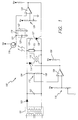
- Figure 1 is a schematic circuit -diagram showing in general one implementation of the flash device 100 according to the present invention.
- the flash device 100 has a flash tube 103 which is connected across the nodes 104 and 106. Also connected across the nodes 104 and 106 is a capacitor 102 and a charging circuit 101 for charging the capacitor 102.
- the capacitor 102 can be a polarized capacitor which can accept an electrical charge at only one polarity (e.g., when the voltage at node 104 is positive with respect to node 106). If a polarized capacitor is not used, a rectifying circuit, such as a diode 103 shown in Figure.1, can be connected between the charging circuit 101 and the capacitor 102.
- a triggering circuit which, according to this embodiment, includes a comparator circuit 108.
- a negative input of the comparator circuit 108 is connected to a reference voltage, which is derived from a voltage source through a voltage divider 110.
- a positive input of the comparator circuit 108 is connected through a voltage divider 112 to monitor the voltage at node 104.
- the output of the comparator circuit 108 is used to control a current switch, such as a SCR 114.
- Resistor 109 at the output of the comparator circuit 108 is a pull-up resistor and is needed only when the comparator circuit 108 is implemented with a certain technology (e.g., open-collector).
- line 30 shows the voltage across the charging capacitor 102.
- the SCR 114 is activated by the output of the comparator circuit 108.
- the SCR 114 passes a current through the primary winding of a trigger transformer 116.
- a high triggering voltage is present at the secondary winding of the trigger transformer 116.
- This high voltage ionizes the gas in flash tube 103 and permits discharge of the energy stored in capacitor 102.
- the gas in the flash tube 103 is ionized, it discharges the electric charge stored in capacitor 102 and emits light.
- the light energy produced by the flash tube 103 increases, as shown at time t1 of line 34 in Figure 2b and line 42 at time t1 in Figure 2d, which shows the line 34 with the timing scale expanded by about 20 times.
- the voltage at node 104 begins to drop, as shown in line 30 of Figure 2a.
- the light emitted from the flash tube 103 is monitored by a monitoring device.
- the monitoring device includes a photo detector, such as a photo transistor 118, which senses the light emitted from the flash tube 103 and produces an electric current in response thereto.
- a photo detector such as a photo transistor 118
- the current produced by the photo transistor 118 begins to increase, as shown in line 34 of Figure 2b and line 42 of Figure 2d between time t1-t2.
- the energy produced by the photo transistor 118 is accumulated, such as by integrating the electric current from the photo transistor 118 by an integrator circuit 119, formed by a capacitor 120 and a resistor 122 connected in parallel.
- the output of the integrator circuit 119 which is the voltage at node 121, represents a time integral of current produced by the photo transistor 118. As current continues to be produced by the photo transistor 118, the voltage at the output of the integrator 119 increases, as shown in line 40 of Figure 2c. Since the current produced by the photo transistor 118 is a function of the light intensity of the flash tube 103, the output of the integrator circuit 119 is a time integral of the light intensity from the flash tube 103. In other words, the output of the integrator circuit 119 represents the total amount of light produced by the flash tube 103 and will increase as current is produced by the photo transistor 118.
- the flash tube 103 when the total amount of light emitted from the flash tube 103 has exceeded a required level, the flash tube 103 can be shut off from the capacitor 102.
- This ideal implementation has two advantages. The first advantage is that the electric charge remaining in the capacitor 102 can be preserved for the subsequent flash.
- the second advantage is that, if the electric current to the flash tube 103 can be immediately cut off, degradation of the flash tube 103 due to the above-described reasons can be stopped immediately. However, because of the high discharge voltage, instantaneous shut-off of the flash tube 103 is not practical. Therefore, in the preferred embodiment, instead of completely shutting off the flash tube 103, the electric current to the flash tube 103 is shunted to reduce the above degradation thereto.
- the photo transistor 118 continues to produce electric current, and the voltage at node 121, the output of the integrator 119, continues to rise, as shown in line 40 of Figure 2c.
- the voltage at the output of the integrator circuit 119 is applied to a positive input of a comparator circuit 124.
- a comparator circuit 124 When the voltage at the positive input of the comparator circuit 124 rises to a predetermined level or threshold (represented by line 38 of Figure 2c) set at the negative input of the comparator circuit 124, an output signal is produced by the comparator circuit 124 to activate a shunting device, such as a SCR 128. This occurs at t2 (see Figure 2c).
- the light energy produced by the flash tube 103 will drop at a faster rate (see line 34 of Figure 2b), as compared to the rate when shunting is not provided (see line 36 of Figure 2b), and the above described degradation of the flash tube 103 is slowed.
- FIG. 3 A presently preferred implementation of the flash circuit 100 is shown in Figure 3.
- An alternating current (A.C.) generator 201 which includes a conventional tickle oscillator formed by transistor 202, resistor 204 and capacitor 206, generates an A.C. signal which is applied to the primary winding of a transformer 208 to provide a step-up voltage at the secondary winding thereof.
- the voltage at the secondary winding of the transformer 208 is applied through a rectifying diode 212 to the charge capacitor 210 connected between nodes 214 and 216.
- the voltage across the charge capacitor 210 is monitored by a voltage divider circuit 217 formed by a resistor 218, a diode 220 and a resistor 222.
- the voltage at the node 223 of the divider circuit 217 is applied to a positive input of a comparator circuit 224.
- the voltage is monitored against a reference voltage which is derived from a voltage source (12VDC) through a divider circuit 225 formed by resistors 226 (which is variable), 228, 230 and 232.
- the output of the comparator circuit 224 is applied to a current switch, such as an SCR 233, through a driver circuit which is formed by resistor 234, transistor 236 and resistor 238.
- a conventional "snubber network" 239 which is formed by a diode 242, capacitor 244 and resistor 246, is used to prevent voltage spikes at the gate of SCR 233.
- SCR 233 When SCR 233 is turned on, it causes a voltage drop at capacitor 248, which is connected to the primary winding of transformer 250.
- the voltage drop at the primary winding of transformer 250 causes a corresponding voltage rise at the secondary winding of transformer 250 which is connected to the trigger electrode 251 of the flash tube 252.
- the voltage at the trigger electrode 251 of the flash tube 252 rises to a predefined level (typically at 15KV)
- the gas in the flash tube 252 is ionized and the flash tube 252 discharges the electric charge stored in capacitor 210, emitting light.
- the light emitted by the flash tube 252 is received by a monitor circuit 264 which includes a photo detector, such as photo transistor 266.
- a photo detector such as photo transistor 266.
- photo transistor 266 produces a current which is a function of the intensity of the light generated by the flash tube 252.
- the normalized magnitude of the current can be controlled by a resistor 278.
- the electric current from photo transistor 266 is integrated by an integrator circuit 268 which includes a resistor 270 and a capacitor 272. As the electric current is integrated, the voltage at the capacitor 272 increases. Thus, the voltage at the capacitor 272 is a function of the intensity of the light as well as the time duration in which the light is emitted.
- the voltage at the capacitor 272 is applied to a first input of a comparator circuit 274.
- the second input of the comparator circuit 274 is connected to a reference voltage provided from the voltage source through a voltage divider circuit which includes a variable resistor 280, and resistors 282, 276 and 232.
- the output of the comparator circuit 274 is used to control a current switch, such as a SCR 284.
- Resistor 286 at the output of the comparator circuit 274 is a pull-up resistor.
- Capacitor 288 and diode 290 together form a snubber circuit to prevent spikes at the gate of SCR 284.
- the voltage at the first input of the comparator circuit 266 rises.
- a signal is produced by the comparator circuit 274 to turn on SCR 284.
- SCR 284 When SCR 284 is turned on, it diverts some of the current from the flash tube 251.
- the current passes through and is thereby dissipated by a resistor 285 (which has a resistance of about 10 ohm in the embodiment).
- a resistor 285 which has a resistance of about 10 ohm in the embodiment.
- the light output would gradually fall as a function of the number of flashes produced, until it is below the preferred level.
- the light output is diyerted in accordance with the present invention, so that it is lower than the maximum as shown in line 7b, but within the preferred levels 7c and 7d, the life span during which the light output remains within the preferred levels 7c and 7d will be extended, as shown in line 7b.
- the flash tube device according to the present invention can be used advantageously for providing flashes of light in apparatuses such as those disclosed in U.S. Patent No. 5,151,595 (the '595 patent), which is incorporated herein by reference.
- FIGS 4a-4c are block diagrams of the imaging devices 10 each of which has a substrate 12 bearing an infrared image producing layer 13 (for example, see the '595 patent).
- the light source of the imaging device 10 is provided by a flash tube device which embodies the present invention.
- the flash tube device includes a flash tube 14 which receives electrical energy from a source of electricity 16 and emits a flash of visible light in response thereto to cause latent heat properties of the infrared layer 13 to convert visible light into far infrared light.
- the flash of visible light is generated as described above by charging a capacitor (not shown) within the electrical source 16 to a predetermined voltage.
- a trigger signal is applied by a trigger circuit 18 to the trigger electrode of the flash tube 14 and to cause the flash tube 14 to discharge.
- the flash tube 14 emits a visible flash of light.
- the light emitted by the flash tube 14 is monitored by a monitor circuit 22.
- the monitor circuit 22 can monitor the light either by sensing the light directly from the flash tube 16 as shown in Figure 4a, or by sensing a reflection of the light from the substrate 12 as shown in Figure 4b. If the light is monitored by sensing light reflected from the substrate 12, a special area 26, not covered by the infrared image producing layer 13, is reserved on the substrate 12 to provide the reflection. This is to ensure that the light is reflected from an area having a predetermined reflectivity unaffected by the layer 13.
- a photo-reactive material 24 such as a photo chromic material, which can change the wavelength.of the light in real-time. Changes in the photo-reactive material is then sensed by a sensing device 28 which sends a signal to the monitor circuit 22 in response thereto.
- the monitor circuit 22 When the monitor circuit 22 detects that a predetermined amount of light has been emitted from the flash tube 14, it activates a circuit 20 to reduce the electrical energy supplied to the flash tube 14.
- the electrical energy supplied to flash tube 14 is reduced by diverting some of the electric current away from the flash tube 14, and dissipating the current, for example, by a shunt resistor.
- the amount of light to be generated from the flash tube 14 can be fixed by fixing the time during which light is emitted from the flash tube.
- the light emitted from the flash tube 14 is received by a monitor device 22' which starts a timer in response to the emitted light.
- a signal is sent to the shunt circuit 20 to divert the electric current from the flash tube 14.
- An alternative technique for prolonging the effective life span of the flash tube is to set the charge voltage of the charge capacitor to the minimum required level.
- the charge voltage is initially set so that the flash tube emits just 1500 BWPS.
- a counter 21 is provided to count the number of flashes produced from the flash tube 14. This can be accomplished by either monitoring the light emitted from the flash tube 14 or the number of times the flash tube 14 has been charged/discharged.
- the counter 21 is connected to a circuit 19 which operates to increase the charge voltage of the charge capacitor.
- the charge voltage is automatically increased as a function of the flashes already produced by the flash tube 14 (e.g., -raising the reference voltage of the trigger circuit by m volt when the flash tube has produced n flashes).
- increasing the charge voltage can be accomplished by raising the reference voltage of the trigger circuit.
- this implementation will not control the amount of light from the tube in a controlled manner over the life of the flash tube 14.
Landscapes
- Discharge-Lamp Control Circuits And Pulse- Feed Circuits (AREA)
Applications Claiming Priority (2)
| Application Number | Priority Date | Filing Date | Title |
|---|---|---|---|
| US306865 | 1994-09-15 | ||
| US08/306,865 US5497001A (en) | 1994-09-15 | 1994-09-15 | Flash tube devices |
Publications (1)
| Publication Number | Publication Date |
|---|---|
| EP0702507A1 true EP0702507A1 (en) | 1996-03-20 |
Family
ID=23187208
Family Applications (1)
| Application Number | Title | Priority Date | Filing Date |
|---|---|---|---|
| EP95113405A Withdrawn EP0702507A1 (en) | 1994-09-15 | 1995-08-25 | Flash tube devices |
Country Status (11)
| Country | Link |
|---|---|
| US (2) | US5497001A (pt) |
| EP (1) | EP0702507A1 (pt) |
| JP (1) | JPH08203690A (pt) |
| KR (1) | KR960013138A (pt) |
| CN (1) | CN1139746A (pt) |
| AU (1) | AU3022295A (pt) |
| BR (1) | BR9504674A (pt) |
| CA (1) | CA2157077A1 (pt) |
| IE (1) | IE950723A1 (pt) |
| PT (1) | PT101769A (pt) |
| TW (1) | TW423784U (pt) |
Families Citing this family (8)
| Publication number | Priority date | Publication date | Assignee | Title |
|---|---|---|---|---|
| US5962984A (en) * | 1998-01-12 | 1999-10-05 | Morris W. Mashburn, III | High intensity lighting circuit |
| US6278382B1 (en) * | 1998-11-06 | 2001-08-21 | Demarco Ralph Anthony | Recognition/anti-collision light for aircraft |
| US6624585B2 (en) * | 2001-09-10 | 2003-09-23 | Infocus Corporation | Ultra-compact igniter circuit for arc discharge lamp |
| WO2006023212A2 (en) * | 2004-07-26 | 2006-03-02 | Thermal Wave Imaging | Infrared camera measurement correction for pulsed excitation with subframe duration |
| JP4666976B2 (ja) * | 2004-08-18 | 2011-04-06 | キヤノン株式会社 | 閃光装置およびカメラ |
| GB2477546B (en) * | 2010-02-05 | 2013-06-19 | Dezac Group Ltd | Skin treatment apparatus |
| SE535271C2 (sv) * | 2010-07-20 | 2012-06-12 | Profoto Ab | Blixtanordning och ett förfarande för att styra färgtemperaturen hos ljuset i en blixt |
| JP6053298B2 (ja) * | 2012-03-08 | 2016-12-27 | キヤノン株式会社 | 眼科装置及び眼科装置の制御方法 |
Citations (5)
| Publication number | Priority date | Publication date | Assignee | Title |
|---|---|---|---|---|
| US4330737A (en) * | 1980-01-21 | 1982-05-18 | Vivitar Corporation | Electronic flash system |
| US4336481A (en) * | 1979-10-26 | 1982-06-22 | Fuji Photo Optical Co., Ltd. | Method of and apparatus for automatic electronic flash lamp control |
| US4382211A (en) * | 1979-11-07 | 1983-05-03 | Fuji Koeki Corporation | Electric flash device |
| DE3500087A1 (de) * | 1984-03-29 | 1985-07-18 | Olympus Optical Co., Ltd., Tokio/Tokyo | Elektronenblitzgeraet mit reihensteuerung |
| US5151595A (en) | 1990-10-16 | 1992-09-29 | Simon Marketing, Inc. | Imaging device and method for developing, duplicating and printing graphic media |
Family Cites Families (6)
| Publication number | Priority date | Publication date | Assignee | Title |
|---|---|---|---|---|
| US3033988A (en) * | 1957-04-05 | 1962-05-08 | Edgerton Germeshausen & Grier | Method of and apparatus for the control of electric impulses |
| US3350604A (en) * | 1965-06-01 | 1967-10-31 | Honeywell Inc | Flash lamp controlled by photosensitive light integrating device |
| US3684917A (en) * | 1969-09-22 | 1972-08-15 | Asahi Optical Co Ltd | Photo flash intensity control with preparatory flash controlling partial discharge of main capacitor |
| US3648104A (en) * | 1969-10-03 | 1972-03-07 | Bosch Photokino Gmbh | Electronic flash unit with preliminary flash for automatic timing |
| US4249109A (en) * | 1979-01-04 | 1981-02-03 | Rollei Of America, Inc. | Light digitizing circuit for an electronic flash device |
| JPH03276782A (ja) * | 1990-03-27 | 1991-12-06 | Matsushita Electric Ind Co Ltd | パルス光源 |
-
1994
- 1994-09-15 US US08/306,865 patent/US5497001A/en not_active Expired - Fee Related
-
1995
- 1995-08-25 EP EP95113405A patent/EP0702507A1/en not_active Withdrawn
- 1995-08-25 AU AU30222/95A patent/AU3022295A/en not_active Abandoned
- 1995-08-28 CA CA002157077A patent/CA2157077A1/en not_active Abandoned
- 1995-09-14 IE IE950723A patent/IE950723A1/en not_active IP Right Cessation
- 1995-09-14 CN CN95116246A patent/CN1139746A/zh active Pending
- 1995-09-14 PT PT101769A patent/PT101769A/pt not_active Application Discontinuation
- 1995-09-14 KR KR1019950030062A patent/KR960013138A/ko not_active Ceased
- 1995-09-15 BR BR9504674A patent/BR9504674A/pt not_active Application Discontinuation
- 1995-09-18 JP JP7238760A patent/JPH08203690A/ja active Pending
- 1995-11-04 TW TW085208493U patent/TW423784U/zh unknown
-
1996
- 1996-02-07 US US08/597,928 patent/US5705808A/en not_active Expired - Fee Related
Patent Citations (5)
| Publication number | Priority date | Publication date | Assignee | Title |
|---|---|---|---|---|
| US4336481A (en) * | 1979-10-26 | 1982-06-22 | Fuji Photo Optical Co., Ltd. | Method of and apparatus for automatic electronic flash lamp control |
| US4382211A (en) * | 1979-11-07 | 1983-05-03 | Fuji Koeki Corporation | Electric flash device |
| US4330737A (en) * | 1980-01-21 | 1982-05-18 | Vivitar Corporation | Electronic flash system |
| DE3500087A1 (de) * | 1984-03-29 | 1985-07-18 | Olympus Optical Co., Ltd., Tokio/Tokyo | Elektronenblitzgeraet mit reihensteuerung |
| US5151595A (en) | 1990-10-16 | 1992-09-29 | Simon Marketing, Inc. | Imaging device and method for developing, duplicating and printing graphic media |
Also Published As
| Publication number | Publication date |
|---|---|
| PT101769A (pt) | 1996-05-31 |
| CN1139746A (zh) | 1997-01-08 |
| US5497001A (en) | 1996-03-05 |
| KR960013138A (ko) | 1996-04-20 |
| AU3022295A (en) | 1996-03-28 |
| TW423784U (en) | 2001-02-21 |
| IE950723A1 (en) | 1996-03-20 |
| US5705808A (en) | 1998-01-06 |
| BR9504674A (pt) | 1997-05-27 |
| CA2157077A1 (en) | 1996-03-16 |
| JPH08203690A (ja) | 1996-08-09 |
Similar Documents
| Publication | Publication Date | Title |
|---|---|---|
| US5313247A (en) | Flash device | |
| US4255046A (en) | Variable output power supply for flash unit | |
| US5497001A (en) | Flash tube devices | |
| US4228381A (en) | Flash tube apparatus with delayed emission | |
| US6009281A (en) | Flash device | |
| US6630798B2 (en) | Electronic flash device of automatic light adjusting type | |
| EP0035224B1 (en) | Electronic flash apparatus | |
| US3634725A (en) | Modulated electronic flash control | |
| US5668445A (en) | Electronic flash apparatus with constant duration repeated flash | |
| US4298826A (en) | Automatic flash unit | |
| JPH0862681A (ja) | 閃光発光装置 | |
| EP0146599B1 (en) | Electronic photoflash control circuit | |
| US4158155A (en) | Ignition circuit for extinguishing tubes in electronic flash equipment | |
| US4602194A (en) | Exciting circuit for electronic flash device | |
| US4561751A (en) | Flash device | |
| US4155031A (en) | Electronic flash apparatus | |
| JPH08320514A (ja) | 閃光撮影装置 | |
| JP3111095B2 (ja) | 炎検出装置 | |
| US20040233323A1 (en) | [A FlashLIGHT CONTROL DEVICE AND An OPERATING method thereof] | |
| JP3490202B2 (ja) | 容量放電式点火装置 | |
| JPH06163179A (ja) | 閃光発光装置 | |
| JP3159735B2 (ja) | 赤目防止装置 | |
| JP2002156690A (ja) | フラット発光可能なストロボ装置 | |
| JPS5943678Y2 (ja) | 電子閃光装置 | |
| JPS60159837A (ja) | 複写機用フラッシュ露光装置 |
Legal Events
| Date | Code | Title | Description |
|---|---|---|---|
| PUAI | Public reference made under article 153(3) epc to a published international application that has entered the european phase |
Free format text: ORIGINAL CODE: 0009012 |
|
| AK | Designated contracting states |
Kind code of ref document: A1 Designated state(s): AT BE DE ES FR GB IT NL |
|
| 17P | Request for examination filed |
Effective date: 19960813 |
|
| 17Q | First examination report despatched |
Effective date: 19971107 |
|
| STAA | Information on the status of an ep patent application or granted ep patent |
Free format text: STATUS: THE APPLICATION IS DEEMED TO BE WITHDRAWN |
|
| 18D | Application deemed to be withdrawn |
Effective date: 19980519 |