EP0703619A1 - Procédé pour fabriquer un circuit intégré tridimensionnel pour atteindre des systèmes à rendement plus haut - Google Patents
Procédé pour fabriquer un circuit intégré tridimensionnel pour atteindre des systèmes à rendement plus haut Download PDFInfo
- Publication number
- EP0703619A1 EP0703619A1 EP95113435A EP95113435A EP0703619A1 EP 0703619 A1 EP0703619 A1 EP 0703619A1 EP 95113435 A EP95113435 A EP 95113435A EP 95113435 A EP95113435 A EP 95113435A EP 0703619 A1 EP0703619 A1 EP 0703619A1
- Authority
- EP
- European Patent Office
- Prior art keywords
- substrate
- component
- circuits
- components
- chips
- Prior art date
- Legal status (The legal status is an assumption and is not a legal conclusion. Google has not performed a legal analysis and makes no representation as to the accuracy of the status listed.)
- Granted
Links
Images
Classifications
-
- H—ELECTRICITY
- H10—SEMICONDUCTOR DEVICES; ELECTRIC SOLID-STATE DEVICES NOT OTHERWISE PROVIDED FOR
- H10W—GENERIC PACKAGES, INTERCONNECTIONS, CONNECTORS OR OTHER CONSTRUCTIONAL DETAILS OF DEVICES COVERED BY CLASS H10
- H10W90/00—Package configurations
-
- H—ELECTRICITY
- H10—SEMICONDUCTOR DEVICES; ELECTRIC SOLID-STATE DEVICES NOT OTHERWISE PROVIDED FOR
- H10D—INORGANIC ELECTRIC SEMICONDUCTOR DEVICES
- H10D86/00—Integrated devices formed in or on insulating or conducting substrates, e.g. formed in silicon-on-insulator [SOI] substrates or on stainless steel or glass substrates
-
- H—ELECTRICITY
- H10—SEMICONDUCTOR DEVICES; ELECTRIC SOLID-STATE DEVICES NOT OTHERWISE PROVIDED FOR
- H10D—INORGANIC ELECTRIC SEMICONDUCTOR DEVICES
- H10D86/00—Integrated devices formed in or on insulating or conducting substrates, e.g. formed in silicon-on-insulator [SOI] substrates or on stainless steel or glass substrates
- H10D86/01—Manufacture or treatment
-
- H—ELECTRICITY
- H10—SEMICONDUCTOR DEVICES; ELECTRIC SOLID-STATE DEVICES NOT OTHERWISE PROVIDED FOR
- H10W—GENERIC PACKAGES, INTERCONNECTIONS, CONNECTORS OR OTHER CONSTRUCTIONAL DETAILS OF DEVICES COVERED BY CLASS H10
- H10W20/00—Interconnections in chips, wafers or substrates
- H10W20/01—Manufacture or treatment
- H10W20/021—Manufacture or treatment of interconnections within wafers or substrates
- H10W20/023—Manufacture or treatment of interconnections within wafers or substrates the interconnections being through-semiconductor vias
- H10W20/0234—Manufacture or treatment of interconnections within wafers or substrates the interconnections being through-semiconductor vias comprising etching via holes that stop on pads or on electrodes
-
- H—ELECTRICITY
- H10—SEMICONDUCTOR DEVICES; ELECTRIC SOLID-STATE DEVICES NOT OTHERWISE PROVIDED FOR
- H10P—GENERIC PROCESSES OR APPARATUS FOR THE MANUFACTURE OR TREATMENT OF DEVICES COVERED BY CLASS H10
- H10P72/00—Handling or holding of wafers, substrates or devices during manufacture or treatment thereof
- H10P72/70—Handling or holding of wafers, substrates or devices during manufacture or treatment thereof for supporting or gripping
- H10P72/74—Handling or holding of wafers, substrates or devices during manufacture or treatment thereof for supporting or gripping using temporarily an auxiliary support
- H10P72/743—Handling or holding of wafers, substrates or devices during manufacture or treatment thereof for supporting or gripping using temporarily an auxiliary support used as a support during manufacture of interconnect decals or build up layers
-
- H—ELECTRICITY
- H10—SEMICONDUCTOR DEVICES; ELECTRIC SOLID-STATE DEVICES NOT OTHERWISE PROVIDED FOR
- H10W—GENERIC PACKAGES, INTERCONNECTIONS, CONNECTORS OR OTHER CONSTRUCTIONAL DETAILS OF DEVICES COVERED BY CLASS H10
- H10W90/00—Package configurations
- H10W90/20—Configurations of stacked chips
- H10W90/297—Configurations of stacked chips characterised by the through-semiconductor vias [TSVs] in the stacked chips
-
- H—ELECTRICITY
- H10—SEMICONDUCTOR DEVICES; ELECTRIC SOLID-STATE DEVICES NOT OTHERWISE PROVIDED FOR
- H10W—GENERIC PACKAGES, INTERCONNECTIONS, CONNECTORS OR OTHER CONSTRUCTIONAL DETAILS OF DEVICES COVERED BY CLASS H10
- H10W90/00—Package configurations
- H10W90/701—Package configurations characterised by the relative positions of pads or connectors relative to package parts
- H10W90/721—Package configurations characterised by the relative positions of pads or connectors relative to package parts of bump connectors
- H10W90/722—Package configurations characterised by the relative positions of pads or connectors relative to package parts of bump connectors between stacked chips
Definitions
- the invention relates to a method for producing a three-dimensional integrated circuit while achieving high system yields.
- Three-dimensional integration is the vertical connection of components that were manufactured using planar technology.
- the advantages of a three-dimensionally integrated microelectronic system include the higher packing densities and switching speeds that can be achieved with the same design rules compared to two-dimensional systems. The latter is due, on the one hand, to shorter line paths between the individual components or circuits, and, on the other hand, to the possibility of parallel information processing.
- the increase in the performance of the system is optimal when implementing a connection technology with freely selectable, highly integrable vertical contacts.
- Y. Akasaka, Proc. IEEE 74 (1986) 1703 proposes to deposit and recrystallize polycrystalline silicon on a completely processed component layer, so that further components can be produced in the recrystallized layer.
- Disadvantages of this method are the yield-reducing degradation of the components in the lower level due to the high thermal load during the recrystallization process, and the necessary serial processing of the overall system. The latter, on the one hand, necessitates correspondingly long throughput times in production and, on the other hand, results in a reduction in yield by adding up the process-related failures. Both increase the manufacturing costs considerably compared to processing the individual levels separately from one another in different substrates.
- CMOS complementary metal-oxide-semiconductor
- No. 4,939,568 describes a method for producing a three-dimensional integrated circuit structure by stacking individual ICs to form a single chip stack on a carrier substrate.
- a substrate with finished ICs is first divided into individual chips, which ends the processing at the wafer level.
- the chips are tested and a first single chip is applied to a carrier substrate by means of thermal compression. After this step, another chip is applied to the first chip in the same way.
- a first chip stack is thus first completed before the production of a further chip stack on another carrier substrate is started. Further processing of the chip stack at the wafer level is therefore not possible with this method.
- a major disadvantage of the previously mentioned methods is due to the fact that the devices available in silicon technology only allow processing (processing) of disk-shaped substrates, the so-called wafers.
- a processing of different substrates, especially of individual chips, is only possible in experimental test plants, but not in the context of industrial production with the required high yields.
- No. 4,954,875 describes a method for three-dimensional integration by stacking individual wafers, in which the connection of the individual component levels is established via specially shaped vias.
- the resultant yield of a multilayer system results from the product of the individual yields.
- the yield of a system comprising several component levels drops drastically according to the known processes.
- the yield of a component substrate also depends on the type of circuits and the manufacturing process used. For example, very high yields in the production of memory chips, while a significantly lower yield is achieved with logic chips, such as microprocessors. In particular, if several types of such circuits are stacked on top of one another, the overall yield is determined disproportionately by the type of circuit with the lowest yield.
- the invention is based on the object of specifying a method for producing a three-dimensional integrated circuit with which a clear increase in yield compared to previously known methods is achieved using the usual industrial standard equipment at the wafer level.
- an additional carrier substrate which does not contain any component structures is used to build up a system comprising a plurality of component levels.
- a fully processed substrate which comprises circuit structures and metallization levels, is subjected to a functional test with which the intact chips of the substrate are selected.
- This substrate is then connected to an auxiliary substrate, thinned from the rear and broken down into individual chips.
- the substrate region below the oxide layer can also be removed in the case of an SOI substrate.
- Selected, intact chips are then connected to the carrier substrate, for example via an adhesive layer, the individual chips being arranged next to one another in a predetermined scheme. The chips are thus assembled on the carrier substrate to form a new chip level. In this way, a wafer is provided which contains only intact components and circuits in the component level.
- the (divided) auxiliary substrate is removed.
- a planarization step is now preferably inserted (claim 9). After that, the substrate, which only contains tested and functional chips in the component level, can be processed further in common manufacturing plants.
- the planarization can be carried out using various methods. First, an insulation layer, such as. B. spin-on glass or a CVD oxide, applied to fill the trenches. The surface is then leveled, which is done by etching back, mechanical or chemomechanical grinding.
- an insulation layer such as. B. spin-on glass or a CVD oxide
- a further component level is applied, for example in the same way, in chips and the surface is planarized (claim 2).
- the electrical connection between a metallization of the upper and lower component levels is then established, for example, via vias (claim 10), which were already introduced into the chips during the processing of the individual substrates and are now etched through to a metallization level of the component level below.
- the structuring of the photomask on each individual chip is adjusted separately using adjustment structures in order to compensate for any dimensional deviations caused by the application of the individual chips and to achieve high adjustment accuracy.
- the existing partial stack i.e. the original carrier substrate with all previously applied component levels
- the existing partial stack i.e. the original carrier substrate with all previously applied component levels
- the functional chips are connected to a new carrier substrate via an adhesive layer, the auxiliary substrates are removed and the surface is planarized.
- a further component level is applied in chips, the surface is planarized and the electrical connection is established.
- the number of levels that are applied is not limited in this method. In addition, not only a single level, but also a partial stack that already consists of several levels can be applied in chips.
- monocrystalline or polycrystalline silicon substrates which are provided with an insulating layer, such as e.g. Silicon oxide can be provided, other materials that are compatible with semiconductor processes, such as e.g. Quartz or glass substrates. It is advantageous if the thermal expansion coefficients of the carrier substrate and the component substrate are adapted in order to keep mechanical stresses low due to temperature cycles caused by process steps. Since the component substrates used already comprise metallization levels which usually contain aluminum or an aluminum alloy, the subsequent process steps are generally restricted to maximum temperatures of approximately 400 ° C.
- the adhesive layer can function as a buffer layer for reducing mechanical stress or as a passivation layer (claim 7). Furthermore, the adhesive layer can bring about a planarization of the surface (claim 8).
- An organic material such as e.g. Polyimide or photoresist can be used.
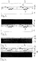
- a first component substrate 1 made of, for example, monocrystalline silicon comprises a plurality of, usually identical, chips 2 arranged according to a defined scheme, the circuit structures 3, such as a MOS transistor, and contain one or more metallization levels 4, which typically consist of aluminum, an aluminum alloy or other materials, such as copper or tungsten, and for electrical insulation are surrounded by an oxide layer 5, which can also be doped with boron and / or phosphorus for planarization purposes .
- the top metallization level 4 can also be covered by a passivation layer 6 made of, for example, silicon oxide and silicon nitride.
- adjustment structures for the precise joining of several levels are implemented (not shown in FIG. 1).
- the substrate has a thickness of, for example, 625 ⁇ m. This component substrate represents the lower substrate of the multilayer system (FIG. 1).
- the passivation 6 is opened at the top metallization level at certain measuring points.
- the individual chips of the substrate are then subjected to a functional test and the defective chips are identified (e.g. with an inkjet).
- a passivation layer is then applied again in order to protect the exposed measuring points again.
- This adhesive layer 7 with a thickness of typically 1-2 ⁇ m can also cause a planarization of the surface.
- the auxiliary substrate 8 is used as a handling substrate for the further process steps and protects the surface of the component substrate 1 during further processing. (Fig. 2).
- the component substrate 1 is thinned from the back by etching and / or grinding, so that the thickness of the substrate 1 below the circuit structures 3 is only a few micrometers, typically 1-5 ⁇ m, is. The selected remaining thickness also depends on the type of circuits contained.
- a carrier substrate 9, e.g. consists of mono- or polycrystalline silicon and possibly covered with an insulation layer 10, such as silicon oxide, does not contain any circuit structures.
- the component substrate 1 with the handling substrate 8 is divided into individual chips. This can be done with an etching process, by sawing or with a laser.
- the marked, intact chips 2 are then applied next to one another in a predetermined arrangement on the carrier substrate 9.
- the handling substrate 8 is then removed by etching or grinding, and the exposed adhesive layer 7 is typically removed over the entire area using an oxygen plasma or a solvent.
- the surface of the carrier substrate 9 with the component substrates 1 now has trenches between the individual chips 2 which have a very low aspect ratio.
- the layer 12 e.g. CVD oxide
- the passivation layer 6 can serve as a stop layer for the etching back or grinding back.
- the carrier substrate 9 with the applied first component level can now be further processed like a conventional silicon substrate with standard technology devices (FIG. 4).
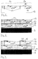
- a second component substrate 13 likewise comprises a plurality of, usually identical, chips 14 arranged according to a defined scheme, which contain circuit structures 15, such as a MOS transistor, and one or more metallization levels 16.
- This substrate 13 is constructed essentially similarly to the first component substrate 1, but the circuit structures 15 are generally different in their function.
- the second component substrate has via holes 17 at the locations on which the electrical contact to the underlying circuit structures is to be made later. The via holes 17 are so deep that they extend to below the layer with circuit structures 15 (FIG. 5).
- This component substrate 13 is also subjected to a functional test, the defective chips are identified, and an adhesive layer and an auxiliary substrate are applied in a similar manner.
- the component substrate 13 is likewise thinned from the back to the via holes 17 by etching and / or grinding.
- the second component substrate 13 with the handling substrate is now divided into individual chips and the marked, intact chips 14 are aligned on the carrier substrate 9, provided with an adhesive layer 18, with the first component level 1.
- the adhesive layer 18 with a thickness of typically 1-2 ⁇ m can cause a planarization of the surface.
- the handling substrate is then removed by etching or grinding and the exposed adhesive layer is removed over the entire surface. Then, after layer 19 has been deposited (for example CVD oxide), a planarization step is also carried out, with which a flat surface is produced (FIG. 6).
- the vertical connection 20 is established between a metallization level 16 of the upper component level (substrate 13) and a metallization level 4 of the lower component level (substrate 1).
- a contact hole to a metallization level 16 of the upper component level and the prepared via holes 17 to a metallization level 4 of the lower component level are opened with a photolithography step and an electrical connection 20 is realized by metal deposition and structuring.
- a passivation layer 21 is deposited on the surface (FIG. 7).
- the electrical contact can of course also be implemented in a different way, for example when the chips are being applied to the lower substrate by means of prepared front and rear contacts (cf. introduction to the description: Y. Hayashi et al.).
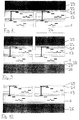
- the already implemented system consisting of two layers is subjected to a function test and the defective chips are identified.
- a passivation layer is then deposited over the entire surface to protect the surface.
- An adhesive layer 22 and an auxiliary substrate 23 are then applied in the manner already illustrated.
- the carrier substrate 9 including the insulation layer 10 and the adhesive layer 11 under the first component level (substrate 1) are finally z. B. removed by etching and / or grinding from the back (Fig. 8).
- the carrier substrate can also be removed, for example, by etching away the adhesive layer 11 and then used again as a carrier substrate for subsequent process steps (claim 4).
- the auxiliary substrate 23 is now divided into individual chips (partial stacks) 24 together with the two component levels, whereupon the marked, intact chips are adjusted and applied to a new carrier substrate 26, which may be provided with an insulation layer 27 and with an adhesive layer 28 (FIG . 9).
- the handling substrates 25 are then removed by etching and / or grinding and the exposed adhesive layer 22 is removed over the entire area. Then, after layer 29 (e.g. CVD oxide) has been deposited, a planarization step is also carried out, with which a flat surface is produced. A substrate is thus obtained which contains only fully functional chips with two component levels (FIG. 10).
- layer 29 e.g. CVD oxide
Landscapes
- Testing Or Measuring Of Semiconductors Or The Like (AREA)
- Internal Circuitry In Semiconductor Integrated Circuit Devices (AREA)
Applications Claiming Priority (2)
| Application Number | Priority Date | Filing Date | Title |
|---|---|---|---|
| DE4433833 | 1994-09-22 | ||
| DE4433833A DE4433833A1 (de) | 1994-09-22 | 1994-09-22 | Verfahren zur Herstellung einer dreidimensionalen integrierten Schaltung unter Erreichung hoher Systemausbeuten |
Publications (2)
| Publication Number | Publication Date |
|---|---|
| EP0703619A1 true EP0703619A1 (fr) | 1996-03-27 |
| EP0703619B1 EP0703619B1 (fr) | 1999-11-03 |
Family
ID=6528893
Family Applications (1)
| Application Number | Title | Priority Date | Filing Date |
|---|---|---|---|
| EP95113435A Expired - Lifetime EP0703619B1 (fr) | 1994-09-22 | 1995-08-26 | Procédé pour fabriquer un circuit intégré tridimensionnel pour atteindre des systèmes à rendement plus haut |
Country Status (4)
| Country | Link |
|---|---|
| US (1) | US5877034A (fr) |
| EP (1) | EP0703619B1 (fr) |
| JP (1) | JPH08204123A (fr) |
| DE (2) | DE4433833A1 (fr) |
Cited By (9)
| Publication number | Priority date | Publication date | Assignee | Title |
|---|---|---|---|---|
| WO1998002921A1 (fr) * | 1996-07-11 | 1998-01-22 | Kopin Corporation | Circuit integre flexible transfere |
| WO2000074136A1 (fr) * | 1999-05-31 | 2000-12-07 | Fraunhofer-Gesellschaft zur Förderung der angewandten Forschung e.V. | Procede de production de circuits tridimensionnels |
| WO2003041167A1 (fr) * | 2001-11-05 | 2003-05-15 | Mitsumasa Koyanagi | Dispositif semi-conducteur comprenant un film en materiau a constante dielectrique faible et procede de fabrication associe |
| DE10200399A1 (de) * | 2002-01-08 | 2003-07-24 | Advanced Micro Devices Inc | Dreidimensional integrierte Halbleitervorrichtung |
| EP0975472A4 (fr) * | 1997-04-04 | 2007-07-04 | Glenn J Leedy | Memoire a structure tridimensionnelle |
| US7265402B2 (en) | 2001-11-05 | 2007-09-04 | Zycube Co., Ltd. | Solid-state image sensor including a microlens |
| US7385835B2 (en) | 1992-04-08 | 2008-06-10 | Elm Technology Corporation | Membrane 3D IC fabrication |
| US7474004B2 (en) | 1997-04-04 | 2009-01-06 | Elm Technology Corporation | Three dimensional structure memory |
| CN113544827A (zh) * | 2021-05-21 | 2021-10-22 | 广东省科学院半导体研究所 | 一种芯片的封装方法及封装结构 |
Families Citing this family (222)
| Publication number | Priority date | Publication date | Assignee | Title |
|---|---|---|---|---|
| DE19516487C1 (de) * | 1995-05-05 | 1996-07-25 | Fraunhofer Ges Forschung | Verfahren zur vertikalen Integration mikroelektronischer Systeme |
| DE19543540C1 (de) * | 1995-11-22 | 1996-11-21 | Siemens Ag | Vertikal integriertes Halbleiterbauelement mit zwei miteinander verbundenen Substraten und Herstellungsverfahren dafür |
| US6342434B1 (en) * | 1995-12-04 | 2002-01-29 | Hitachi, Ltd. | Methods of processing semiconductor wafer, and producing IC card, and carrier |
| US5998291A (en) * | 1997-04-07 | 1999-12-07 | Raytheon Company | Attachment method for assembly of high density multiple interconnect structures |
| DE19746641B4 (de) * | 1997-09-19 | 2006-02-23 | Fraunhofer-Gesellschaft zur Förderung der angewandten Forschung e.V. | Verdrahtungsverfahren für Halbleiter-Bauelemente zur Verhinderung von Produktpiraterie und Produktmanipulation und Verwendung des Halbleiter-Bauelements in einer Chipkarte |
| DE19813239C1 (de) * | 1998-03-26 | 1999-12-23 | Fraunhofer Ges Forschung | Verdrahtungsverfahren zur Herstellung einer vertikalen integrierten Schaltungsstruktur und vertikale integrierte Schaltungsstruktur |
| DE19853703A1 (de) * | 1998-11-20 | 2000-05-25 | Giesecke & Devrient Gmbh | Verfahren zur Herstellung eines beidseitig prozessierten integrierten Schaltkreises |
| DE19856573C1 (de) | 1998-12-08 | 2000-05-18 | Fraunhofer Ges Forschung | Verfahren zur vertikalen Integration von aktiven Schaltungsebenen und unter Verwendung desselben erzeugte vertikale integrierte Schaltung |
| EP1041624A1 (fr) * | 1999-04-02 | 2000-10-04 | Interuniversitair Microelektronica Centrum Vzw | Methode de transfert de substrates ultra-minces et mis en oeuvre de sa methode dans la fabrication de dispositifs de type couches minces |
| US6984571B1 (en) * | 1999-10-01 | 2006-01-10 | Ziptronix, Inc. | Three dimensional device integration method and integrated device |
| US6500694B1 (en) * | 2000-03-22 | 2002-12-31 | Ziptronix, Inc. | Three dimensional device integration method and integrated device |
| US6882045B2 (en) * | 1999-10-28 | 2005-04-19 | Thomas J. Massingill | Multi-chip module and method for forming and method for deplating defective capacitors |
| DE19954941C2 (de) * | 1999-11-16 | 2003-11-06 | Fraunhofer Ges Forschung | Verfahren zum Integrieren eines Chips innerhalb einer Leiterplatte |
| US6902987B1 (en) | 2000-02-16 | 2005-06-07 | Ziptronix, Inc. | Method for low temperature bonding and bonded structure |
| US6743697B2 (en) * | 2000-06-30 | 2004-06-01 | Intel Corporation | Thin silicon circuits and method for making the same |
| US6627998B1 (en) * | 2000-07-27 | 2003-09-30 | International Business Machines Corporation | Wafer scale thin film package |
| KR100537552B1 (ko) * | 2000-07-31 | 2005-12-16 | 매그나칩 반도체 유한회사 | 반도체 소자 및 그의 제조 방법 |
| US6563133B1 (en) * | 2000-08-09 | 2003-05-13 | Ziptronix, Inc. | Method of epitaxial-like wafer bonding at low temperature and bonded structure |
| US6774010B2 (en) | 2001-01-25 | 2004-08-10 | International Business Machines Corporation | Transferable device-containing layer for silicon-on-insulator applications |
| WO2004015764A2 (fr) | 2002-08-08 | 2004-02-19 | Leedy Glenn J | Integration de systeme verticale |
| WO2004061953A2 (fr) * | 2002-12-31 | 2004-07-22 | Massachusetts Institute Of Technology | Procede de realisation d'une structure de semi-conducteurs multicouches integrant un tenon de traitement |
| US7064055B2 (en) * | 2002-12-31 | 2006-06-20 | Massachusetts Institute Of Technology | Method of forming a multi-layer semiconductor structure having a seamless bonding interface |
| US20040124538A1 (en) * | 2002-12-31 | 2004-07-01 | Rafael Reif | Multi-layer integrated semiconductor structure |
| JP4063082B2 (ja) * | 2003-01-10 | 2008-03-19 | 日本電気株式会社 | フレキシブル電子デバイスとその製造方法 |
| TWI328837B (en) * | 2003-02-28 | 2010-08-11 | Semiconductor Energy Lab | Semiconductor device and method of manufacturing the same |
| KR100497111B1 (ko) * | 2003-03-25 | 2005-06-28 | 삼성전자주식회사 | 웨이퍼 레벨 칩 스케일 패키지, 그를 적층한 적층 패키지및 그 제조 방법 |
| US7109092B2 (en) | 2003-05-19 | 2006-09-19 | Ziptronix, Inc. | Method of room temperature covalent bonding |
| DE10323394B4 (de) * | 2003-05-20 | 2006-09-28 | Fraunhofer-Gesellschaft zur Förderung der angewandten Forschung e.V. | Verfahren zum Erzeugen einer elektrischen Kontaktierung zwischen zwei Halbleiterstücken und Verfahren zum Herstellen einer Anordnung von Halbleiterstücken |
| JP2005123463A (ja) | 2003-10-17 | 2005-05-12 | Seiko Epson Corp | 半導体装置及びその製造方法、半導体装置モジュール、回路基板並びに電子機器 |
| DE102004056970B4 (de) * | 2004-11-25 | 2008-07-03 | Fraunhofer-Gesellschaft zur Förderung der angewandten Forschung e.V. | Verfahren und Vorrichtung zum Erzeugen einer elektrischen Kontaktierung zwischen zwei Halbleiterstücken durch ein mechanisches Element |
| US8153511B2 (en) * | 2005-05-30 | 2012-04-10 | Semiconductor Energy Laboratory Co., Ltd. | Method for manufacturing semiconductor device |
| AT503191B1 (de) | 2006-02-02 | 2008-07-15 | Austria Tech & System Tech | Leiterplattenelement mit wenigstens einem eingebetteten bauelement sowie verfahren zum einbetten zumindest eines bauelements in einem leiterplattenelement |
| JP4659660B2 (ja) * | 2006-03-31 | 2011-03-30 | Okiセミコンダクタ株式会社 | 半導体装置の製造方法 |
| US7408798B2 (en) * | 2006-03-31 | 2008-08-05 | International Business Machines Corporation | 3-dimensional integrated circuit architecture, structure and method for fabrication thereof |
| US7684224B2 (en) * | 2006-03-31 | 2010-03-23 | International Business Machines Corporation | Structure comprising 3-dimensional integrated circuit architecture, circuit structure, and instructions for fabrication thereof |
| US20070279053A1 (en) * | 2006-05-12 | 2007-12-06 | Taylor William P | Integrated current sensor |
| US7880278B2 (en) | 2006-05-16 | 2011-02-01 | Taiwan Semiconductor Manufacturing Company, Ltd. | Integrated circuit having stress tuning layer |
| US7851333B2 (en) * | 2007-03-15 | 2010-12-14 | Infineon Technologies Ag | Apparatus comprising a device and method for producing it |
| US7615480B2 (en) * | 2007-06-20 | 2009-11-10 | Lam Research Corporation | Methods of post-contact back end of the line through-hole via integration |
| US8193092B2 (en) * | 2007-07-31 | 2012-06-05 | Micron Technology, Inc. | Semiconductor devices including a through-substrate conductive member with an exposed end and methods of manufacturing such semiconductor devices |
| JP2009076879A (ja) | 2007-08-24 | 2009-04-09 | Semiconductor Energy Lab Co Ltd | 半導体装置 |
| US8232598B2 (en) * | 2007-09-20 | 2012-07-31 | Semiconductor Energy Laboratory Co., Ltd. | Display device and method for manufacturing the same |
| US7982250B2 (en) * | 2007-09-21 | 2011-07-19 | Semiconductor Energy Laboratory Co., Ltd. | Semiconductor device |
| US8044464B2 (en) * | 2007-09-21 | 2011-10-25 | Semiconductor Energy Laboratory Co., Ltd. | Semiconductor device |
| US8536629B2 (en) * | 2009-02-24 | 2013-09-17 | Nec Corporation | Semiconductor device and method for manufacturing the same |
| US12027518B1 (en) | 2009-10-12 | 2024-07-02 | Monolithic 3D Inc. | 3D semiconductor devices and structures with metal layers |
| US10354995B2 (en) | 2009-10-12 | 2019-07-16 | Monolithic 3D Inc. | Semiconductor memory device and structure |
| US11374118B2 (en) | 2009-10-12 | 2022-06-28 | Monolithic 3D Inc. | Method to form a 3D integrated circuit |
| US10157909B2 (en) | 2009-10-12 | 2018-12-18 | Monolithic 3D Inc. | 3D semiconductor device and structure |
| US11018133B2 (en) | 2009-10-12 | 2021-05-25 | Monolithic 3D Inc. | 3D integrated circuit |
| US10366970B2 (en) | 2009-10-12 | 2019-07-30 | Monolithic 3D Inc. | 3D semiconductor device and structure |
| US11984445B2 (en) | 2009-10-12 | 2024-05-14 | Monolithic 3D Inc. | 3D semiconductor devices and structures with metal layers |
| US10910364B2 (en) | 2009-10-12 | 2021-02-02 | Monolitaic 3D Inc. | 3D semiconductor device |
| US10388863B2 (en) | 2009-10-12 | 2019-08-20 | Monolithic 3D Inc. | 3D memory device and structure |
| US10043781B2 (en) | 2009-10-12 | 2018-08-07 | Monolithic 3D Inc. | 3D semiconductor device and structure |
| US10217667B2 (en) | 2011-06-28 | 2019-02-26 | Monolithic 3D Inc. | 3D semiconductor device, fabrication method and system |
| US10497713B2 (en) | 2010-11-18 | 2019-12-03 | Monolithic 3D Inc. | 3D semiconductor memory device and structure |
| US11482440B2 (en) | 2010-12-16 | 2022-10-25 | Monolithic 3D Inc. | 3D semiconductor device and structure with a built-in test circuit for repairing faulty circuits |
| US12362219B2 (en) | 2010-11-18 | 2025-07-15 | Monolithic 3D Inc. | 3D semiconductor memory device and structure |
| US10290682B2 (en) | 2010-10-11 | 2019-05-14 | Monolithic 3D Inc. | 3D IC semiconductor device and structure with stacked memory |
| US11600667B1 (en) | 2010-10-11 | 2023-03-07 | Monolithic 3D Inc. | Method to produce 3D semiconductor devices and structures with memory |
| US11018191B1 (en) | 2010-10-11 | 2021-05-25 | Monolithic 3D Inc. | 3D semiconductor device and structure |
| US11158674B2 (en) | 2010-10-11 | 2021-10-26 | Monolithic 3D Inc. | Method to produce a 3D semiconductor device and structure |
| US11257867B1 (en) | 2010-10-11 | 2022-02-22 | Monolithic 3D Inc. | 3D semiconductor device and structure with oxide bonds |
| US11315980B1 (en) | 2010-10-11 | 2022-04-26 | Monolithic 3D Inc. | 3D semiconductor device and structure with transistors |
| US10896931B1 (en) | 2010-10-11 | 2021-01-19 | Monolithic 3D Inc. | 3D semiconductor device and structure |
| US11024673B1 (en) | 2010-10-11 | 2021-06-01 | Monolithic 3D Inc. | 3D semiconductor device and structure |
| US11227897B2 (en) | 2010-10-11 | 2022-01-18 | Monolithic 3D Inc. | Method for producing a 3D semiconductor memory device and structure |
| US11469271B2 (en) | 2010-10-11 | 2022-10-11 | Monolithic 3D Inc. | Method to produce 3D semiconductor devices and structures with memory |
| US12080743B2 (en) | 2010-10-13 | 2024-09-03 | Monolithic 3D Inc. | Multilevel semiconductor device and structure with image sensors and wafer bonding |
| US10998374B1 (en) | 2010-10-13 | 2021-05-04 | Monolithic 3D Inc. | Multilevel semiconductor device and structure |
| US11605663B2 (en) | 2010-10-13 | 2023-03-14 | Monolithic 3D Inc. | Multilevel semiconductor device and structure with image sensors and wafer bonding |
| US11163112B2 (en) | 2010-10-13 | 2021-11-02 | Monolithic 3D Inc. | Multilevel semiconductor device and structure with electromagnetic modulators |
| US10679977B2 (en) | 2010-10-13 | 2020-06-09 | Monolithic 3D Inc. | 3D microdisplay device and structure |
| US11855114B2 (en) | 2010-10-13 | 2023-12-26 | Monolithic 3D Inc. | Multilevel semiconductor device and structure with image sensors and wafer bonding |
| US10978501B1 (en) | 2010-10-13 | 2021-04-13 | Monolithic 3D Inc. | Multilevel semiconductor device and structure with waveguides |
| US11164898B2 (en) | 2010-10-13 | 2021-11-02 | Monolithic 3D Inc. | Multilevel semiconductor device and structure |
| US12094892B2 (en) | 2010-10-13 | 2024-09-17 | Monolithic 3D Inc. | 3D micro display device and structure |
| US11984438B2 (en) | 2010-10-13 | 2024-05-14 | Monolithic 3D Inc. | Multilevel semiconductor device and structure with oxide bonding |
| US11063071B1 (en) | 2010-10-13 | 2021-07-13 | Monolithic 3D Inc. | Multilevel semiconductor device and structure with waveguides |
| US11929372B2 (en) | 2010-10-13 | 2024-03-12 | Monolithic 3D Inc. | Multilevel semiconductor device and structure with image sensors and wafer bonding |
| US11855100B2 (en) | 2010-10-13 | 2023-12-26 | Monolithic 3D Inc. | Multilevel semiconductor device and structure with oxide bonding |
| US11404466B2 (en) | 2010-10-13 | 2022-08-02 | Monolithic 3D Inc. | Multilevel semiconductor device and structure with image sensors |
| US12360310B2 (en) | 2010-10-13 | 2025-07-15 | Monolithic 3D Inc. | Multilevel semiconductor device and structure with oxide bonding |
| US11133344B2 (en) | 2010-10-13 | 2021-09-28 | Monolithic 3D Inc. | Multilevel semiconductor device and structure with image sensors |
| US11694922B2 (en) | 2010-10-13 | 2023-07-04 | Monolithic 3D Inc. | Multilevel semiconductor device and structure with oxide bonding |
| US11327227B2 (en) | 2010-10-13 | 2022-05-10 | Monolithic 3D Inc. | Multilevel semiconductor device and structure with electromagnetic modulators |
| US10833108B2 (en) | 2010-10-13 | 2020-11-10 | Monolithic 3D Inc. | 3D microdisplay device and structure |
| US10943934B2 (en) | 2010-10-13 | 2021-03-09 | Monolithic 3D Inc. | Multilevel semiconductor device and structure |
| US11869915B2 (en) | 2010-10-13 | 2024-01-09 | Monolithic 3D Inc. | Multilevel semiconductor device and structure with image sensors and wafer bonding |
| US11437368B2 (en) | 2010-10-13 | 2022-09-06 | Monolithic 3D Inc. | Multilevel semiconductor device and structure with oxide bonding |
| US11043523B1 (en) | 2010-10-13 | 2021-06-22 | Monolithic 3D Inc. | Multilevel semiconductor device and structure with image sensors |
| US11164770B1 (en) | 2010-11-18 | 2021-11-02 | Monolithic 3D Inc. | Method for producing a 3D semiconductor memory device and structure |
| US11901210B2 (en) | 2010-11-18 | 2024-02-13 | Monolithic 3D Inc. | 3D semiconductor device and structure with memory |
| US12243765B2 (en) | 2010-11-18 | 2025-03-04 | Monolithic 3D Inc. | 3D semiconductor device and structure with metal layers and memory cells |
| US11521888B2 (en) | 2010-11-18 | 2022-12-06 | Monolithic 3D Inc. | 3D semiconductor device and structure with high-k metal gate transistors |
| US11482439B2 (en) | 2010-11-18 | 2022-10-25 | Monolithic 3D Inc. | Methods for producing a 3D semiconductor memory device comprising charge trap junction-less transistors |
| US11211279B2 (en) | 2010-11-18 | 2021-12-28 | Monolithic 3D Inc. | Method for processing a 3D integrated circuit and structure |
| US11615977B2 (en) | 2010-11-18 | 2023-03-28 | Monolithic 3D Inc. | 3D semiconductor memory device and structure |
| US11355381B2 (en) | 2010-11-18 | 2022-06-07 | Monolithic 3D Inc. | 3D semiconductor memory device and structure |
| US12033884B2 (en) | 2010-11-18 | 2024-07-09 | Monolithic 3D Inc. | Methods for producing a 3D semiconductor device and structure with memory cells and multiple metal layers |
| US11004719B1 (en) | 2010-11-18 | 2021-05-11 | Monolithic 3D Inc. | Methods for producing a 3D semiconductor memory device and structure |
| US11804396B2 (en) | 2010-11-18 | 2023-10-31 | Monolithic 3D Inc. | Methods for producing a 3D semiconductor device and structure with memory cells and multiple metal layers |
| US11862503B2 (en) | 2010-11-18 | 2024-01-02 | Monolithic 3D Inc. | Method for producing a 3D semiconductor device and structure with memory cells and multiple metal layers |
| US11094576B1 (en) | 2010-11-18 | 2021-08-17 | Monolithic 3D Inc. | Methods for producing a 3D semiconductor memory device and structure |
| US11923230B1 (en) | 2010-11-18 | 2024-03-05 | Monolithic 3D Inc. | 3D semiconductor device and structure with bonding |
| US11355380B2 (en) | 2010-11-18 | 2022-06-07 | Monolithic 3D Inc. | Methods for producing 3D semiconductor memory device and structure utilizing alignment marks |
| US11031275B2 (en) | 2010-11-18 | 2021-06-08 | Monolithic 3D Inc. | 3D semiconductor device and structure with memory |
| US11495484B2 (en) | 2010-11-18 | 2022-11-08 | Monolithic 3D Inc. | 3D semiconductor devices and structures with at least two single-crystal layers |
| US11735462B2 (en) | 2010-11-18 | 2023-08-22 | Monolithic 3D Inc. | 3D semiconductor device and structure with single-crystal layers |
| US12144190B2 (en) | 2010-11-18 | 2024-11-12 | Monolithic 3D Inc. | 3D semiconductor device and structure with bonding and memory cells preliminary class |
| US11610802B2 (en) | 2010-11-18 | 2023-03-21 | Monolithic 3D Inc. | Method for producing a 3D semiconductor device and structure with single crystal transistors and metal gate electrodes |
| US12125737B1 (en) | 2010-11-18 | 2024-10-22 | Monolithic 3D Inc. | 3D semiconductor device and structure with metal layers and memory cells |
| US11482438B2 (en) | 2010-11-18 | 2022-10-25 | Monolithic 3D Inc. | Methods for producing a 3D semiconductor memory device and structure |
| US11854857B1 (en) | 2010-11-18 | 2023-12-26 | Monolithic 3D Inc. | Methods for producing a 3D semiconductor device and structure with memory cells and multiple metal layers |
| US12272586B2 (en) | 2010-11-18 | 2025-04-08 | Monolithic 3D Inc. | 3D semiconductor memory device and structure with memory and metal layers |
| US11508605B2 (en) | 2010-11-18 | 2022-11-22 | Monolithic 3D Inc. | 3D semiconductor memory device and structure |
| US11443971B2 (en) | 2010-11-18 | 2022-09-13 | Monolithic 3D Inc. | 3D semiconductor device and structure with memory |
| US11121021B2 (en) | 2010-11-18 | 2021-09-14 | Monolithic 3D Inc. | 3D semiconductor device and structure |
| US11107721B2 (en) | 2010-11-18 | 2021-08-31 | Monolithic 3D Inc. | 3D semiconductor device and structure with NAND logic |
| US12100611B2 (en) | 2010-11-18 | 2024-09-24 | Monolithic 3D Inc. | Methods for producing a 3D semiconductor device and structure with memory cells and multiple metal layers |
| US11569117B2 (en) | 2010-11-18 | 2023-01-31 | Monolithic 3D Inc. | 3D semiconductor device and structure with single-crystal layers |
| US11784082B2 (en) | 2010-11-18 | 2023-10-10 | Monolithic 3D Inc. | 3D semiconductor device and structure with bonding |
| US11018042B1 (en) | 2010-11-18 | 2021-05-25 | Monolithic 3D Inc. | 3D semiconductor memory device and structure |
| US12136562B2 (en) | 2010-11-18 | 2024-11-05 | Monolithic 3D Inc. | 3D semiconductor device and structure with single-crystal layers |
| US12068187B2 (en) | 2010-11-18 | 2024-08-20 | Monolithic 3D Inc. | 3D semiconductor device and structure with bonding and DRAM memory cells |
| US12154817B1 (en) | 2010-11-18 | 2024-11-26 | Monolithic 3D Inc. | Methods for producing a 3D semiconductor memory device and structure |
| US12463076B2 (en) | 2010-12-16 | 2025-11-04 | Monolithic 3D Inc. | 3D semiconductor device and structure |
| DE102011013228B4 (de) * | 2011-03-07 | 2014-05-28 | Austriamicrosystems Ag | Verfahren zur Herstellung eines Halbleiterbauelements für 3D-Integration |
| US10388568B2 (en) | 2011-06-28 | 2019-08-20 | Monolithic 3D Inc. | 3D semiconductor device and system |
| DE102012200258A1 (de) | 2012-01-10 | 2013-07-11 | Fraunhofer-Gesellschaft zur Förderung der angewandten Forschung e.V. | Verfahren zur herstellung eines chips |
| US11594473B2 (en) | 2012-04-09 | 2023-02-28 | Monolithic 3D Inc. | 3D semiconductor device and structure with metal layers and a connective path |
| US11694944B1 (en) | 2012-04-09 | 2023-07-04 | Monolithic 3D Inc. | 3D semiconductor device and structure with metal layers and a connective path |
| US11164811B2 (en) | 2012-04-09 | 2021-11-02 | Monolithic 3D Inc. | 3D semiconductor device with isolation layers and oxide-to-oxide bonding |
| US11410912B2 (en) | 2012-04-09 | 2022-08-09 | Monolithic 3D Inc. | 3D semiconductor device with vias and isolation layers |
| US11616004B1 (en) | 2012-04-09 | 2023-03-28 | Monolithic 3D Inc. | 3D semiconductor device and structure with metal layers and a connective path |
| US11881443B2 (en) | 2012-04-09 | 2024-01-23 | Monolithic 3D Inc. | 3D semiconductor device and structure with metal layers and a connective path |
| US11476181B1 (en) | 2012-04-09 | 2022-10-18 | Monolithic 3D Inc. | 3D semiconductor device and structure with metal layers |
| US10600888B2 (en) | 2012-04-09 | 2020-03-24 | Monolithic 3D Inc. | 3D semiconductor device |
| US11735501B1 (en) | 2012-04-09 | 2023-08-22 | Monolithic 3D Inc. | 3D semiconductor device and structure with metal layers and a connective path |
| US11088050B2 (en) | 2012-04-09 | 2021-08-10 | Monolithic 3D Inc. | 3D semiconductor device with isolation layers |
| US11967583B2 (en) | 2012-12-22 | 2024-04-23 | Monolithic 3D Inc. | 3D semiconductor device and structure with metal layers |
| US11063024B1 (en) | 2012-12-22 | 2021-07-13 | Monlithic 3D Inc. | Method to form a 3D semiconductor device and structure |
| US12051674B2 (en) | 2012-12-22 | 2024-07-30 | Monolithic 3D Inc. | 3D semiconductor device and structure with metal layers |
| US11018116B2 (en) | 2012-12-22 | 2021-05-25 | Monolithic 3D Inc. | Method to form a 3D semiconductor device and structure |
| US11916045B2 (en) | 2012-12-22 | 2024-02-27 | Monolithic 3D Inc. | 3D semiconductor device and structure with metal layers |
| US11784169B2 (en) | 2012-12-22 | 2023-10-10 | Monolithic 3D Inc. | 3D semiconductor device and structure with metal layers |
| US11309292B2 (en) | 2012-12-22 | 2022-04-19 | Monolithic 3D Inc. | 3D semiconductor device and structure with metal layers |
| US11961827B1 (en) | 2012-12-22 | 2024-04-16 | Monolithic 3D Inc. | 3D semiconductor device and structure with metal layers |
| US11217565B2 (en) | 2012-12-22 | 2022-01-04 | Monolithic 3D Inc. | Method to form a 3D semiconductor device and structure |
| US10115663B2 (en) | 2012-12-29 | 2018-10-30 | Monolithic 3D Inc. | 3D semiconductor device and structure |
| US11430668B2 (en) | 2012-12-29 | 2022-08-30 | Monolithic 3D Inc. | 3D semiconductor device and structure with bonding |
| US10651054B2 (en) | 2012-12-29 | 2020-05-12 | Monolithic 3D Inc. | 3D semiconductor device and structure |
| US11087995B1 (en) | 2012-12-29 | 2021-08-10 | Monolithic 3D Inc. | 3D semiconductor device and structure |
| US12249538B2 (en) | 2012-12-29 | 2025-03-11 | Monolithic 3D Inc. | 3D semiconductor device and structure including power distribution grids |
| US10600657B2 (en) | 2012-12-29 | 2020-03-24 | Monolithic 3D Inc | 3D semiconductor device and structure |
| US11177140B2 (en) | 2012-12-29 | 2021-11-16 | Monolithic 3D Inc. | 3D semiconductor device and structure |
| US11430667B2 (en) | 2012-12-29 | 2022-08-30 | Monolithic 3D Inc. | 3D semiconductor device and structure with bonding |
| US10903089B1 (en) | 2012-12-29 | 2021-01-26 | Monolithic 3D Inc. | 3D semiconductor device and structure |
| US10892169B2 (en) | 2012-12-29 | 2021-01-12 | Monolithic 3D Inc. | 3D semiconductor device and structure |
| US11004694B1 (en) | 2012-12-29 | 2021-05-11 | Monolithic 3D Inc. | 3D semiconductor device and structure |
| US8902663B1 (en) | 2013-03-11 | 2014-12-02 | Monolithic 3D Inc. | Method of maintaining a memory state |
| US11935949B1 (en) | 2013-03-11 | 2024-03-19 | Monolithic 3D Inc. | 3D semiconductor device and structure with metal layers and memory cells |
| US12094965B2 (en) | 2013-03-11 | 2024-09-17 | Monolithic 3D Inc. | 3D semiconductor device and structure with metal layers and memory cells |
| US11869965B2 (en) | 2013-03-11 | 2024-01-09 | Monolithic 3D Inc. | 3D semiconductor device and structure with metal layers and memory cells |
| US10325651B2 (en) | 2013-03-11 | 2019-06-18 | Monolithic 3D Inc. | 3D semiconductor device with stacked memory |
| US11923374B2 (en) | 2013-03-12 | 2024-03-05 | Monolithic 3D Inc. | 3D semiconductor device and structure with metal layers |
| US11088130B2 (en) | 2014-01-28 | 2021-08-10 | Monolithic 3D Inc. | 3D semiconductor device and structure |
| US12100646B2 (en) | 2013-03-12 | 2024-09-24 | Monolithic 3D Inc. | 3D semiconductor device and structure with metal layers |
| US10840239B2 (en) | 2014-08-26 | 2020-11-17 | Monolithic 3D Inc. | 3D semiconductor device and structure |
| US11398569B2 (en) | 2013-03-12 | 2022-07-26 | Monolithic 3D Inc. | 3D semiconductor device and structure |
| US10224279B2 (en) | 2013-03-15 | 2019-03-05 | Monolithic 3D Inc. | Semiconductor device and structure |
| US11574109B1 (en) | 2013-04-15 | 2023-02-07 | Monolithic 3D Inc | Automation methods for 3D integrated circuits and devices |
| US11720736B2 (en) | 2013-04-15 | 2023-08-08 | Monolithic 3D Inc. | Automation methods for 3D integrated circuits and devices |
| US9021414B1 (en) | 2013-04-15 | 2015-04-28 | Monolithic 3D Inc. | Automation for monolithic 3D devices |
| US11030371B2 (en) | 2013-04-15 | 2021-06-08 | Monolithic 3D Inc. | Automation for monolithic 3D devices |
| US11341309B1 (en) | 2013-04-15 | 2022-05-24 | Monolithic 3D Inc. | Automation for monolithic 3D devices |
| US11270055B1 (en) | 2013-04-15 | 2022-03-08 | Monolithic 3D Inc. | Automation for monolithic 3D devices |
| US11487928B2 (en) | 2013-04-15 | 2022-11-01 | Monolithic 3D Inc. | Automation for monolithic 3D devices |
| JP2014090186A (ja) * | 2013-12-04 | 2014-05-15 | Semiconductor Energy Lab Co Ltd | 半導体装置の作製方法 |
| US11107808B1 (en) | 2014-01-28 | 2021-08-31 | Monolithic 3D Inc. | 3D semiconductor device and structure |
| US11031394B1 (en) | 2014-01-28 | 2021-06-08 | Monolithic 3D Inc. | 3D semiconductor device and structure |
| US10297586B2 (en) | 2015-03-09 | 2019-05-21 | Monolithic 3D Inc. | Methods for processing a 3D semiconductor device |
| US12094829B2 (en) | 2014-01-28 | 2024-09-17 | Monolithic 3D Inc. | 3D semiconductor device and structure |
| US12477752B2 (en) | 2015-09-21 | 2025-11-18 | Monolithic 3D Inc. | 3D semiconductor memory devices and structures |
| US11114464B2 (en) | 2015-10-24 | 2021-09-07 | Monolithic 3D Inc. | 3D semiconductor device and structure |
| US11056468B1 (en) | 2015-04-19 | 2021-07-06 | Monolithic 3D Inc. | 3D semiconductor device and structure |
| US11296115B1 (en) | 2015-10-24 | 2022-04-05 | Monolithic 3D Inc. | 3D semiconductor device and structure |
| US10825779B2 (en) | 2015-04-19 | 2020-11-03 | Monolithic 3D Inc. | 3D semiconductor device and structure |
| US12035531B2 (en) | 2015-10-24 | 2024-07-09 | Monolithic 3D Inc. | 3D semiconductor device and structure with logic and memory |
| US11937422B2 (en) | 2015-11-07 | 2024-03-19 | Monolithic 3D Inc. | Semiconductor memory device and structure |
| US12219769B2 (en) | 2015-10-24 | 2025-02-04 | Monolithic 3D Inc. | 3D semiconductor device and structure with logic and memory |
| US11011507B1 (en) | 2015-04-19 | 2021-05-18 | Monolithic 3D Inc. | 3D semiconductor device and structure |
| US10847540B2 (en) | 2015-10-24 | 2020-11-24 | Monolithic 3D Inc. | 3D semiconductor memory device and structure |
| US11114427B2 (en) | 2015-11-07 | 2021-09-07 | Monolithic 3D Inc. | 3D semiconductor processor and memory device and structure |
| US10381328B2 (en) | 2015-04-19 | 2019-08-13 | Monolithic 3D Inc. | Semiconductor device and structure |
| US12016181B2 (en) | 2015-10-24 | 2024-06-18 | Monolithic 3D Inc. | 3D semiconductor device and structure with logic and memory |
| US11978731B2 (en) | 2015-09-21 | 2024-05-07 | Monolithic 3D Inc. | Method to produce a multi-level semiconductor memory device and structure |
| US10418369B2 (en) | 2015-10-24 | 2019-09-17 | Monolithic 3D Inc. | Multi-level semiconductor memory device and structure |
| US12615784B2 (en) | 2015-11-07 | 2026-04-28 | Monolithic 3D Inc. | 3D semiconductor memory device and structure |
| US11956952B2 (en) | 2015-08-23 | 2024-04-09 | Monolithic 3D Inc. | Semiconductor memory device and structure |
| DE112016004265T5 (de) | 2015-09-21 | 2018-06-07 | Monolithic 3D Inc. | 3d halbleitervorrichtung und -struktur |
| US12100658B2 (en) | 2015-09-21 | 2024-09-24 | Monolithic 3D Inc. | Method to produce a 3D multilayer semiconductor device and structure |
| US12178055B2 (en) | 2015-09-21 | 2024-12-24 | Monolithic 3D Inc. | 3D semiconductor memory devices and structures |
| US12250830B2 (en) | 2015-09-21 | 2025-03-11 | Monolithic 3D Inc. | 3D semiconductor memory devices and structures |
| US10522225B1 (en) | 2015-10-02 | 2019-12-31 | Monolithic 3D Inc. | Semiconductor device with non-volatile memory |
| US12120880B1 (en) | 2015-10-24 | 2024-10-15 | Monolithic 3D Inc. | 3D semiconductor device and structure with logic and memory |
| US11991884B1 (en) | 2015-10-24 | 2024-05-21 | Monolithic 3D Inc. | 3D semiconductor device and structure with logic and memory |
| US9748106B2 (en) * | 2016-01-21 | 2017-08-29 | Micron Technology, Inc. | Method for fabricating semiconductor package |
| US11329059B1 (en) | 2016-10-10 | 2022-05-10 | Monolithic 3D Inc. | 3D memory devices and structures with thinned single crystal substrates |
| US11251149B2 (en) | 2016-10-10 | 2022-02-15 | Monolithic 3D Inc. | 3D memory device and structure |
| US11930648B1 (en) | 2016-10-10 | 2024-03-12 | Monolithic 3D Inc. | 3D memory devices and structures with metal layers |
| US11812620B2 (en) | 2016-10-10 | 2023-11-07 | Monolithic 3D Inc. | 3D DRAM memory devices and structures with control circuits |
| US11869591B2 (en) | 2016-10-10 | 2024-01-09 | Monolithic 3D Inc. | 3D memory devices and structures with control circuits |
| US11711928B2 (en) | 2016-10-10 | 2023-07-25 | Monolithic 3D Inc. | 3D memory devices and structures with control circuits |
| US12225704B2 (en) | 2016-10-10 | 2025-02-11 | Monolithic 3D Inc. | 3D memory devices and structures with memory arrays and metal layers |
| US10892016B1 (en) | 2019-04-08 | 2021-01-12 | Monolithic 3D Inc. | 3D memory semiconductor devices and structures |
| US11763864B2 (en) | 2019-04-08 | 2023-09-19 | Monolithic 3D Inc. | 3D memory semiconductor devices and structures with bit-line pillars |
| US11296106B2 (en) | 2019-04-08 | 2022-04-05 | Monolithic 3D Inc. | 3D memory semiconductor devices and structures |
| US11158652B1 (en) | 2019-04-08 | 2021-10-26 | Monolithic 3D Inc. | 3D memory semiconductor devices and structures |
| US11018156B2 (en) | 2019-04-08 | 2021-05-25 | Monolithic 3D Inc. | 3D memory semiconductor devices and structures |
| KR20230097121A (ko) | 2020-10-29 | 2023-06-30 | 아데이아 세미컨덕터 본딩 테크놀로지스 인코포레이티드 | 직접 접합 방법 및 구조체 |
Citations (2)
| Publication number | Priority date | Publication date | Assignee | Title |
|---|---|---|---|---|
| EP0531723A1 (fr) * | 1991-09-13 | 1993-03-17 | International Business Machines Corporation | Procédé pour la fabrication de empaquetages tridimensionnels à multi-puces |
| DE4314913C1 (de) * | 1993-05-05 | 1994-08-25 | Siemens Ag | Verfahren zur Herstellung eines Halbleiterbauelements mit einer Kontaktstrukturierung für vertikale Kontaktierung mit weiteren Halbleiterbauelementen |
Family Cites Families (12)
| Publication number | Priority date | Publication date | Assignee | Title |
|---|---|---|---|---|
| KR900008647B1 (ko) * | 1986-03-20 | 1990-11-26 | 후지쓰 가부시끼가이샤 | 3차원 집적회로와 그의 제조방법 |
| US4954875A (en) * | 1986-07-17 | 1990-09-04 | Laser Dynamics, Inc. | Semiconductor wafer array with electrically conductive compliant material |
| US5192716A (en) * | 1989-01-25 | 1993-03-09 | Polylithics, Inc. | Method of making a extended integration semiconductor structure |
| US5104820A (en) * | 1989-07-07 | 1992-04-14 | Irvine Sensors Corporation | Method of fabricating electronic circuitry unit containing stacked IC layers having lead rerouting |
| JPH0344067A (ja) * | 1989-07-11 | 1991-02-25 | Nec Corp | 半導体基板の積層方法 |
| US5256562A (en) * | 1990-12-31 | 1993-10-26 | Kopin Corporation | Method for manufacturing a semiconductor device using a circuit transfer film |
| US5376561A (en) * | 1990-12-31 | 1994-12-27 | Kopin Corporation | High density electronic circuit modules |
| JP3526058B2 (ja) * | 1992-08-19 | 2004-05-10 | セイコーインスツルメンツ株式会社 | 光弁用半導体装置 |
| US5489538A (en) * | 1992-08-21 | 1996-02-06 | Lsi Logic Corporation | Method of die burn-in |
| US5324687A (en) * | 1992-10-16 | 1994-06-28 | General Electric Company | Method for thinning of integrated circuit chips for lightweight packaged electronic systems |
| US5455202A (en) * | 1993-01-19 | 1995-10-03 | Hughes Aircraft Company | Method of making a microelectric device using an alternate substrate |
| US5591678A (en) * | 1993-01-19 | 1997-01-07 | He Holdings, Inc. | Process of manufacturing a microelectric device using a removable support substrate and etch-stop |
-
1994
- 1994-09-22 DE DE4433833A patent/DE4433833A1/de not_active Withdrawn
-
1995
- 1995-08-26 DE DE59507172T patent/DE59507172D1/de not_active Expired - Lifetime
- 1995-08-26 EP EP95113435A patent/EP0703619B1/fr not_active Expired - Lifetime
- 1995-09-22 JP JP7244734A patent/JPH08204123A/ja active Pending
- 1995-09-22 US US08/532,368 patent/US5877034A/en not_active Expired - Lifetime
Patent Citations (2)
| Publication number | Priority date | Publication date | Assignee | Title |
|---|---|---|---|---|
| EP0531723A1 (fr) * | 1991-09-13 | 1993-03-17 | International Business Machines Corporation | Procédé pour la fabrication de empaquetages tridimensionnels à multi-puces |
| DE4314913C1 (de) * | 1993-05-05 | 1994-08-25 | Siemens Ag | Verfahren zur Herstellung eines Halbleiterbauelements mit einer Kontaktstrukturierung für vertikale Kontaktierung mit weiteren Halbleiterbauelementen |
Non-Patent Citations (2)
| Title |
|---|
| T. MORIYA ET AL.: "RESULTS of the three-dimensional integrated circuits project in japan", MICROELECTRONIC ENGINEERING, vol. 15, no. 1/4, October 1991 (1991-10-01), AMSTERDAM, pages 167 - 174, XP000292753, DOI: doi:10.1016/0167-9317(91)90205-R * |
| Y. HAYASHI ET AL.: "a new three dimensional ic fabrication technology, stacking thin film dual-cmos layers", INT. ELECTRON DEVICES MEETING, 8 December 1991 (1991-12-08), WASHINGTON, pages 657 - 660, XP010055229, DOI: doi:10.1109/IEDM.1991.235336 * |
Cited By (23)
| Publication number | Priority date | Publication date | Assignee | Title |
|---|---|---|---|---|
| US7911012B2 (en) | 1992-04-08 | 2011-03-22 | Taiwan Semiconductor Manufacturing Co., Ltd. | Flexible and elastic dielectric integrated circuit |
| US7670893B2 (en) | 1992-04-08 | 2010-03-02 | Taiwan Semiconductor Manufacturing Co., Ltd. | Membrane IC fabrication |
| US7615837B2 (en) | 1992-04-08 | 2009-11-10 | Taiwan Semiconductor Manufacturing Company | Lithography device for semiconductor circuit pattern generation |
| US7485571B2 (en) | 1992-04-08 | 2009-02-03 | Elm Technology Corporation | Method of making an integrated circuit |
| US7479694B2 (en) | 1992-04-08 | 2009-01-20 | Elm Technology Corporation | Membrane 3D IC fabrication |
| US7763948B2 (en) | 1992-04-08 | 2010-07-27 | Taiwan Semiconductor Manufacturing Co., Ltd. | Flexible and elastic dielectric integrated circuit |
| US7385835B2 (en) | 1992-04-08 | 2008-06-10 | Elm Technology Corporation | Membrane 3D IC fabrication |
| US6027958A (en) * | 1996-07-11 | 2000-02-22 | Kopin Corporation | Transferred flexible integrated circuit |
| WO1998002921A1 (fr) * | 1996-07-11 | 1998-01-22 | Kopin Corporation | Circuit integre flexible transfere |
| US7474004B2 (en) | 1997-04-04 | 2009-01-06 | Elm Technology Corporation | Three dimensional structure memory |
| EP0975472A4 (fr) * | 1997-04-04 | 2007-07-04 | Glenn J Leedy | Memoire a structure tridimensionnelle |
| US8035233B2 (en) | 1997-04-04 | 2011-10-11 | Elm Technology Corporation | Adjacent substantially flexible substrates having integrated circuits that are bonded together by non-polymeric layer |
| US7504732B2 (en) | 1997-04-04 | 2009-03-17 | Elm Technology Corporation | Three dimensional structure memory |
| US7705466B2 (en) | 1997-04-04 | 2010-04-27 | Elm Technology Corporation | Three dimensional multi layer memory and control logic integrated circuit structure |
| WO2000074136A1 (fr) * | 1999-05-31 | 2000-12-07 | Fraunhofer-Gesellschaft zur Förderung der angewandten Forschung e.V. | Procede de production de circuits tridimensionnels |
| US7326642B2 (en) | 2001-11-05 | 2008-02-05 | Zycube Co., Ltd. | Method of fabricating semiconductor device using low dielectric constant material film |
| US7265402B2 (en) | 2001-11-05 | 2007-09-04 | Zycube Co., Ltd. | Solid-state image sensor including a microlens |
| US7091534B2 (en) | 2001-11-05 | 2006-08-15 | Zycube Co., Ltd. | Semiconductor device using low dielectric constant material film and method of fabricating the same |
| WO2003041167A1 (fr) * | 2001-11-05 | 2003-05-15 | Mitsumasa Koyanagi | Dispositif semi-conducteur comprenant un film en materiau a constante dielectrique faible et procede de fabrication associe |
| US6943067B2 (en) | 2002-01-08 | 2005-09-13 | Advanced Micro Devices, Inc. | Three-dimensional integrated semiconductor devices |
| DE10200399B4 (de) * | 2002-01-08 | 2008-03-27 | Advanced Micro Devices, Inc., Sunnyvale | Verfahren zur Erzeugung einer dreidimensional integrierten Halbleitervorrichtung und dreidimensional integrierte Halbleitervorrichtung |
| DE10200399A1 (de) * | 2002-01-08 | 2003-07-24 | Advanced Micro Devices Inc | Dreidimensional integrierte Halbleitervorrichtung |
| CN113544827A (zh) * | 2021-05-21 | 2021-10-22 | 广东省科学院半导体研究所 | 一种芯片的封装方法及封装结构 |
Also Published As
| Publication number | Publication date |
|---|---|
| DE59507172D1 (de) | 1999-12-09 |
| DE4433833A1 (de) | 1996-03-28 |
| EP0703619B1 (fr) | 1999-11-03 |
| US5877034A (en) | 1999-03-02 |
| JPH08204123A (ja) | 1996-08-09 |
Similar Documents
| Publication | Publication Date | Title |
|---|---|---|
| EP0703619B1 (fr) | Procédé pour fabriquer un circuit intégré tridimensionnel pour atteindre des systèmes à rendement plus haut | |
| EP0703618B1 (fr) | Procédé pour fabriquer un circuit intégré tridimensionnel | |
| EP0739540B1 (fr) | Procede de fabrication d'un circuit tridimensionnel | |
| DE19543540C1 (de) | Vertikal integriertes Halbleiterbauelement mit zwei miteinander verbundenen Substraten und Herstellungsverfahren dafür | |
| DE112010000142B4 (de) | Kostenoptimiertes Verfahren zum Bilden von hoch dichten passiven Kondensatoren zum Ersetzen diskreter Kondensatoren unter Verwendung eines kostenoptimierten modularen 3D-Wafer-Wafer-Integrationsschemas | |
| DE19813239C1 (de) | Verdrahtungsverfahren zur Herstellung einer vertikalen integrierten Schaltungsstruktur und vertikale integrierte Schaltungsstruktur | |
| DE602004003476T2 (de) | Kondensator, halbleiterbauelement mit einem kondensator und verfahren zur herstellung derselben | |
| DE102016115000B4 (de) | Dreidimensionale integrierte Schaltungs-(3DIC)-Vorrichtung und Verfahren zu deren Herstellung und ein Verfahren zum Bonden von Wafern mittels Hybrid-Bonden | |
| WO2000074134A1 (fr) | Procede d'integration verticale de composants electriques a l'aide d'un contact arriere | |
| EP0703623A1 (fr) | Procédé de fabrication d'une structure de circuit intégré verticale | |
| DE102015205064B4 (de) | Verfahren zum Herstellen von Schaltungselementen | |
| DE102005033916A1 (de) | Ausrichtung eines MTJ-Stapels an Leiterbahnen in Abwesenheit von Topographie | |
| DE102004039906A1 (de) | Verfahren zur Herstellung eines elektronischen Bauelements sowie ein elektronisches Bauelement mit mindestens zwei integrierten Bausteinen | |
| EP1151472B1 (fr) | Procede pour l'integration verticale de plans de circuit actifs | |
| DE102017109670A1 (de) | Chippackage mit Seitenwandmetallisierung | |
| DE10124038A1 (de) | Verfahren zur Herstellung vergrabener Bereiche | |
| DE112011103040T5 (de) | Verfahren zum Ausbilden von Wafer-Durchkontaktierungen in Halbleiterstrukturen unter Verwendung von Opfermaterial und mit diesen Verfahren hergestellte Halbleiterstrukturen | |
| EP1149417B1 (fr) | Procede de production de circuits tridimensionnels | |
| DE102009043740B4 (de) | Rückseitenmetallisierung mit besserer Haftung in Hochleistungshalbleiterbauelementen | |
| DE102023130518A1 (de) | Durchkontaktierungsstruktur und verfahren zur herstellung derselben | |
| DE102023105382A1 (de) | Halbleitervorrichtung und herstellungsverfahren | |
| EP0712154A2 (fr) | Procédé de fabrication de circuits intégrés de haute qualité contenant des composants passifs | |
| EP1183723A1 (fr) | Circuit pouvant etre integre verticalement et son procede de production | |
| DE102017212763A1 (de) | Eine Vorrichtung und ein Verfahren zum Herstellen einer Vorrichtung | |
| DE19958486A1 (de) | Verfahren zur vertikalen Integration von elektrischen Bauelementen mittels Rückseitenkontakt |
Legal Events
| Date | Code | Title | Description |
|---|---|---|---|
| PUAI | Public reference made under article 153(3) epc to a published international application that has entered the european phase |
Free format text: ORIGINAL CODE: 0009012 |
|
| AK | Designated contracting states |
Kind code of ref document: A1 Designated state(s): DE FR GB IE IT |
|
| 17P | Request for examination filed |
Effective date: 19960216 |
|
| 17Q | First examination report despatched |
Effective date: 19970321 |
|
| GRAG | Despatch of communication of intention to grant |
Free format text: ORIGINAL CODE: EPIDOS AGRA |
|
| GRAG | Despatch of communication of intention to grant |
Free format text: ORIGINAL CODE: EPIDOS AGRA |
|
| GRAH | Despatch of communication of intention to grant a patent |
Free format text: ORIGINAL CODE: EPIDOS IGRA |
|
| GRAH | Despatch of communication of intention to grant a patent |
Free format text: ORIGINAL CODE: EPIDOS IGRA |
|
| GRAA | (expected) grant |
Free format text: ORIGINAL CODE: 0009210 |
|
| AK | Designated contracting states |
Kind code of ref document: B1 Designated state(s): DE FR GB IE IT |
|
| GBT | Gb: translation of ep patent filed (gb section 77(6)(a)/1977) |
Effective date: 19991115 |
|
| REF | Corresponds to: |
Ref document number: 59507172 Country of ref document: DE Date of ref document: 19991209 |
|
| ET | Fr: translation filed | ||
| REG | Reference to a national code |
Ref country code: IE Ref legal event code: FG4D Free format text: GERMAN |
|
| ITF | It: translation for a ep patent filed | ||
| PLBE | No opposition filed within time limit |
Free format text: ORIGINAL CODE: 0009261 |
|
| STAA | Information on the status of an ep patent application or granted ep patent |
Free format text: STATUS: NO OPPOSITION FILED WITHIN TIME LIMIT |
|
| 26N | No opposition filed | ||
| REG | Reference to a national code |
Ref country code: GB Ref legal event code: IF02 |
|
| PGFP | Annual fee paid to national office [announced via postgrant information from national office to epo] |
Ref country code: DE Payment date: 20140821 Year of fee payment: 20 Ref country code: IE Payment date: 20140820 Year of fee payment: 20 |
|
| PGFP | Annual fee paid to national office [announced via postgrant information from national office to epo] |
Ref country code: GB Payment date: 20140821 Year of fee payment: 20 Ref country code: FR Payment date: 20140819 Year of fee payment: 20 |
|
| PGFP | Annual fee paid to national office [announced via postgrant information from national office to epo] |
Ref country code: IT Payment date: 20140827 Year of fee payment: 20 |
|
| REG | Reference to a national code |
Ref country code: DE Ref legal event code: R071 Ref document number: 59507172 Country of ref document: DE |
|
| REG | Reference to a national code |
Ref country code: GB Ref legal event code: PE20 Expiry date: 20150825 |
|
| REG | Reference to a national code |
Ref country code: IE Ref legal event code: MK9A |
|
| PG25 | Lapsed in a contracting state [announced via postgrant information from national office to epo] |
Ref country code: GB Free format text: LAPSE BECAUSE OF EXPIRATION OF PROTECTION Effective date: 20150825 Ref country code: IE Free format text: LAPSE BECAUSE OF EXPIRATION OF PROTECTION Effective date: 20150826 |