EP0703626A2 - Struktur mit Resonanztunneleffekt und Herstellungsverfahren - Google Patents
Struktur mit Resonanztunneleffekt und Herstellungsverfahren Download PDFInfo
- Publication number
- EP0703626A2 EP0703626A2 EP95114532A EP95114532A EP0703626A2 EP 0703626 A2 EP0703626 A2 EP 0703626A2 EP 95114532 A EP95114532 A EP 95114532A EP 95114532 A EP95114532 A EP 95114532A EP 0703626 A2 EP0703626 A2 EP 0703626A2
- Authority
- EP
- European Patent Office
- Prior art keywords
- tunneling
- metal
- forming
- nitride
- pmma
- Prior art date
- Legal status (The legal status is an assumption and is not a legal conclusion. Google has not performed a legal analysis and makes no representation as to the accuracy of the status listed.)
- Withdrawn
Links
- 230000005641 tunneling Effects 0.000 title claims abstract description 80
- 238000000034 method Methods 0.000 title claims abstract description 25
- 238000004519 manufacturing process Methods 0.000 title claims abstract description 20
- 230000004888 barrier function Effects 0.000 claims abstract description 46
- 229910052751 metal Inorganic materials 0.000 claims description 73
- 239000002184 metal Substances 0.000 claims description 73
- 229920003229 poly(methyl methacrylate) Polymers 0.000 claims description 46
- 239000004926 polymethyl methacrylate Substances 0.000 claims description 46
- 238000000151 deposition Methods 0.000 claims description 34
- 229920002120 photoresistant polymer Polymers 0.000 claims description 32
- 239000000463 material Substances 0.000 claims description 21
- 229910052782 aluminium Inorganic materials 0.000 claims description 18
- XAGFODPZIPBFFR-UHFFFAOYSA-N aluminium Chemical compound [Al] XAGFODPZIPBFFR-UHFFFAOYSA-N 0.000 claims description 18
- 239000004065 semiconductor Substances 0.000 claims description 13
- RTAQQCXQSZGOHL-UHFFFAOYSA-N Titanium Chemical compound [Ti] RTAQQCXQSZGOHL-UHFFFAOYSA-N 0.000 claims description 7
- 238000005530 etching Methods 0.000 claims description 7
- 239000010936 titanium Substances 0.000 claims description 7
- 229910052719 titanium Inorganic materials 0.000 claims description 7
- 238000010884 ion-beam technique Methods 0.000 claims description 3
- 150000001875 compounds Chemical class 0.000 claims description 2
- 238000000059 patterning Methods 0.000 claims 1
- 238000000638 solvent extraction Methods 0.000 claims 1
- 230000008021 deposition Effects 0.000 abstract description 33
- 239000002096 quantum dot Substances 0.000 abstract description 11
- 238000000926 separation method Methods 0.000 abstract description 5
- 150000004767 nitrides Chemical class 0.000 description 47
- 229910000980 Aluminium gallium arsenide Inorganic materials 0.000 description 36
- JBRZTFJDHDCESZ-UHFFFAOYSA-N AsGa Chemical compound [As]#[Ga] JBRZTFJDHDCESZ-UHFFFAOYSA-N 0.000 description 25
- 229910001218 Gallium arsenide Inorganic materials 0.000 description 24
- 229910000530 Gallium indium arsenide Inorganic materials 0.000 description 24
- 238000005253 cladding Methods 0.000 description 16
- 238000002955 isolation Methods 0.000 description 7
- 239000000758 substrate Substances 0.000 description 7
- NBIIXXVUZAFLBC-UHFFFAOYSA-N Phosphoric acid Chemical compound OP(O)(O)=O NBIIXXVUZAFLBC-UHFFFAOYSA-N 0.000 description 6
- XUIMIQQOPSSXEZ-UHFFFAOYSA-N Silicon Chemical compound [Si] XUIMIQQOPSSXEZ-UHFFFAOYSA-N 0.000 description 5
- QVGXLLKOCUKJST-UHFFFAOYSA-N atomic oxygen Chemical compound [O] QVGXLLKOCUKJST-UHFFFAOYSA-N 0.000 description 5
- 239000001301 oxygen Substances 0.000 description 5
- 229910052760 oxygen Inorganic materials 0.000 description 5
- 229910052710 silicon Inorganic materials 0.000 description 5
- 239000010703 silicon Substances 0.000 description 5
- QGZKDVFQNNGYKY-UHFFFAOYSA-N Ammonia Chemical compound N QGZKDVFQNNGYKY-UHFFFAOYSA-N 0.000 description 4
- XKRFYHLGVUSROY-UHFFFAOYSA-N Argon Chemical compound [Ar] XKRFYHLGVUSROY-UHFFFAOYSA-N 0.000 description 4
- QAOWNCQODCNURD-UHFFFAOYSA-N Sulfuric acid Chemical compound OS(O)(=O)=O QAOWNCQODCNURD-UHFFFAOYSA-N 0.000 description 4
- 239000000460 chlorine Substances 0.000 description 4
- 229910052801 chlorine Inorganic materials 0.000 description 4
- 239000013078 crystal Substances 0.000 description 4
- 238000010586 diagram Methods 0.000 description 4
- 238000004518 low pressure chemical vapour deposition Methods 0.000 description 4
- 238000001883 metal evaporation Methods 0.000 description 4
- 238000001451 molecular beam epitaxy Methods 0.000 description 4
- 229910015844 BCl3 Inorganic materials 0.000 description 3
- ZAMOUSCENKQFHK-UHFFFAOYSA-N Chlorine atom Chemical compound [Cl] ZAMOUSCENKQFHK-UHFFFAOYSA-N 0.000 description 3
- XPDWGBQVDMORPB-UHFFFAOYSA-N Fluoroform Chemical compound FC(F)F XPDWGBQVDMORPB-UHFFFAOYSA-N 0.000 description 3
- 229910000147 aluminium phosphate Inorganic materials 0.000 description 3
- 239000000969 carrier Substances 0.000 description 3
- 230000007547 defect Effects 0.000 description 3
- 230000000694 effects Effects 0.000 description 3
- 238000001459 lithography Methods 0.000 description 3
- 239000000203 mixture Substances 0.000 description 3
- FAQYAMRNWDIXMY-UHFFFAOYSA-N trichloroborane Chemical compound ClB(Cl)Cl FAQYAMRNWDIXMY-UHFFFAOYSA-N 0.000 description 3
- CSCPPACGZOOCGX-UHFFFAOYSA-N Acetone Chemical compound CC(C)=O CSCPPACGZOOCGX-UHFFFAOYSA-N 0.000 description 2
- KLZUFWVZNOTSEM-UHFFFAOYSA-K Aluminium flouride Chemical compound F[Al](F)F KLZUFWVZNOTSEM-UHFFFAOYSA-K 0.000 description 2
- KZBUYRJDOAKODT-UHFFFAOYSA-N Chlorine Chemical compound ClCl KZBUYRJDOAKODT-UHFFFAOYSA-N 0.000 description 2
- MHAJPDPJQMAIIY-UHFFFAOYSA-N Hydrogen peroxide Chemical compound OO MHAJPDPJQMAIIY-UHFFFAOYSA-N 0.000 description 2
- PXHVJJICTQNCMI-UHFFFAOYSA-N Nickel Chemical compound [Ni] PXHVJJICTQNCMI-UHFFFAOYSA-N 0.000 description 2
- BLRPTPMANUNPDV-UHFFFAOYSA-N Silane Chemical compound [SiH4] BLRPTPMANUNPDV-UHFFFAOYSA-N 0.000 description 2
- 229910021529 ammonia Inorganic materials 0.000 description 2
- 229910052786 argon Inorganic materials 0.000 description 2
- 125000004429 atom Chemical group 0.000 description 2
- 230000008901 benefit Effects 0.000 description 2
- 230000015572 biosynthetic process Effects 0.000 description 2
- 238000005229 chemical vapour deposition Methods 0.000 description 2
- 239000002019 doping agent Substances 0.000 description 2
- 239000007943 implant Substances 0.000 description 2
- 238000002488 metal-organic chemical vapour deposition Methods 0.000 description 2
- 238000005036 potential barrier Methods 0.000 description 2
- 230000009467 reduction Effects 0.000 description 2
- 229910000077 silane Inorganic materials 0.000 description 2
- XLYOFNOQVPJJNP-UHFFFAOYSA-N water Substances O XLYOFNOQVPJJNP-UHFFFAOYSA-N 0.000 description 2
- KRHYYFGTRYWZRS-UHFFFAOYSA-M Fluoride anion Chemical compound [F-] KRHYYFGTRYWZRS-UHFFFAOYSA-M 0.000 description 1
- YCKRFDGAMUMZLT-UHFFFAOYSA-N Fluorine atom Chemical compound [F] YCKRFDGAMUMZLT-UHFFFAOYSA-N 0.000 description 1
- 229910052581 Si3N4 Inorganic materials 0.000 description 1
- BYDQGSVXQDOSJJ-UHFFFAOYSA-N [Ge].[Au] Chemical compound [Ge].[Au] BYDQGSVXQDOSJJ-UHFFFAOYSA-N 0.000 description 1
- FTWRSWRBSVXQPI-UHFFFAOYSA-N alumanylidynearsane;gallanylidynearsane Chemical compound [As]#[Al].[As]#[Ga] FTWRSWRBSVXQPI-UHFFFAOYSA-N 0.000 description 1
- MDPILPRLPQYEEN-UHFFFAOYSA-N aluminium arsenide Chemical compound [As]#[Al] MDPILPRLPQYEEN-UHFFFAOYSA-N 0.000 description 1
- 238000013459 approach Methods 0.000 description 1
- 125000001309 chloro group Chemical group Cl* 0.000 description 1
- 230000000295 complement effect Effects 0.000 description 1
- 238000011161 development Methods 0.000 description 1
- 238000004090 dissolution Methods 0.000 description 1
- 238000010894 electron beam technology Methods 0.000 description 1
- 230000003628 erosive effect Effects 0.000 description 1
- 230000001747 exhibiting effect Effects 0.000 description 1
- 229910052731 fluorine Inorganic materials 0.000 description 1
- 239000011737 fluorine Substances 0.000 description 1
- 239000007789 gas Substances 0.000 description 1
- PCHJSUWPFVWCPO-UHFFFAOYSA-N gold Chemical compound [Au] PCHJSUWPFVWCPO-UHFFFAOYSA-N 0.000 description 1
- 239000010931 gold Substances 0.000 description 1
- 229910052737 gold Inorganic materials 0.000 description 1
- 239000002784 hot electron Substances 0.000 description 1
- 238000002164 ion-beam lithography Methods 0.000 description 1
- 238000001465 metallisation Methods 0.000 description 1
- 238000012986 modification Methods 0.000 description 1
- 230000004048 modification Effects 0.000 description 1
- 229910052759 nickel Inorganic materials 0.000 description 1
- 150000002978 peroxides Chemical class 0.000 description 1
- 238000000206 photolithography Methods 0.000 description 1
- 230000008569 process Effects 0.000 description 1
- 238000012545 processing Methods 0.000 description 1
- 230000000717 retained effect Effects 0.000 description 1
- HQVNEWCFYHHQES-UHFFFAOYSA-N silicon nitride Chemical compound N12[Si]34N5[Si]62N3[Si]51N64 HQVNEWCFYHHQES-UHFFFAOYSA-N 0.000 description 1
Images






Classifications
-
- B—PERFORMING OPERATIONS; TRANSPORTING
- B82—NANOTECHNOLOGY
- B82Y—SPECIFIC USES OR APPLICATIONS OF NANOSTRUCTURES; MEASUREMENT OR ANALYSIS OF NANOSTRUCTURES; MANUFACTURE OR TREATMENT OF NANOSTRUCTURES
- B82Y10/00—Nanotechnology for information processing, storage or transmission, e.g. quantum computing or single electron logic
-
- H—ELECTRICITY
- H10—SEMICONDUCTOR DEVICES; ELECTRIC SOLID-STATE DEVICES NOT OTHERWISE PROVIDED FOR
- H10D—INORGANIC ELECTRIC SEMICONDUCTOR DEVICES
- H10D62/00—Semiconductor bodies, or regions thereof, of devices having potential barriers
- H10D62/80—Semiconductor bodies, or regions thereof, of devices having potential barriers characterised by the materials
- H10D62/81—Semiconductor bodies, or regions thereof, of devices having potential barriers characterised by the materials of structures exhibiting quantum-confinement effects, e.g. single quantum wells; of structures having periodic or quasi-periodic potential variation
- H10D62/812—Single quantum well structures
- H10D62/813—Quantum wire structures
-
- H—ELECTRICITY
- H10—SEMICONDUCTOR DEVICES; ELECTRIC SOLID-STATE DEVICES NOT OTHERWISE PROVIDED FOR
- H10D—INORGANIC ELECTRIC SEMICONDUCTOR DEVICES
- H10D62/00—Semiconductor bodies, or regions thereof, of devices having potential barriers
- H10D62/80—Semiconductor bodies, or regions thereof, of devices having potential barriers characterised by the materials
- H10D62/81—Semiconductor bodies, or regions thereof, of devices having potential barriers characterised by the materials of structures exhibiting quantum-confinement effects, e.g. single quantum wells; of structures having periodic or quasi-periodic potential variation
- H10D62/812—Single quantum well structures
- H10D62/814—Quantum box structures
-
- H—ELECTRICITY
- H10—SEMICONDUCTOR DEVICES; ELECTRIC SOLID-STATE DEVICES NOT OTHERWISE PROVIDED FOR
- H10D—INORGANIC ELECTRIC SEMICONDUCTOR DEVICES
- H10D8/00—Diodes
- H10D8/70—Tunnel-effect diodes
- H10D8/755—Resonant tunneling diodes [RTD]
-
- Y—GENERAL TAGGING OF NEW TECHNOLOGICAL DEVELOPMENTS; GENERAL TAGGING OF CROSS-SECTIONAL TECHNOLOGIES SPANNING OVER SEVERAL SECTIONS OF THE IPC; TECHNICAL SUBJECTS COVERED BY FORMER USPC CROSS-REFERENCE ART COLLECTIONS [XRACs] AND DIGESTS
- Y10—TECHNICAL SUBJECTS COVERED BY FORMER USPC
- Y10S—TECHNICAL SUBJECTS COVERED BY FORMER USPC CROSS-REFERENCE ART COLLECTIONS [XRACs] AND DIGESTS
- Y10S438/00—Semiconductor device manufacturing: process
- Y10S438/962—Quantum dots and lines
-
- Y—GENERAL TAGGING OF NEW TECHNOLOGICAL DEVELOPMENTS; GENERAL TAGGING OF CROSS-SECTIONAL TECHNOLOGIES SPANNING OVER SEVERAL SECTIONS OF THE IPC; TECHNICAL SUBJECTS COVERED BY FORMER USPC CROSS-REFERENCE ART COLLECTIONS [XRACs] AND DIGESTS
- Y10—TECHNICAL SUBJECTS COVERED BY FORMER USPC
- Y10S—TECHNICAL SUBJECTS COVERED BY FORMER USPC CROSS-REFERENCE ART COLLECTIONS [XRACs] AND DIGESTS
- Y10S438/00—Semiconductor device manufacturing: process
- Y10S438/979—Tunnel diodes
Definitions
- the invention relates to electronic devices, and, more particularly, to quantum mechanical resonant tunneling devices and systems and fabrication methods.
- Resonant tunneling diodes are two terminal devices with conduction carriers tunneling through potential barriers to yield current-voltage curves with portions exhibiting negative differential resistance. Recall that the original Esaki diode had interband tunneling (e.g., from conduction band to valence band) in a heavily doped PN junction diode.
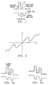
- An alternative resonant tunneling diode structure relies on resonant tunneling through a quantum well in a single band; see Figure 1 which illustrates a AlGaAs/GaAs quantum well.
- U.S.Patent No. 4,912,531 shows lateral resonant tunneling through quantum dots of GaAs surrounded by AlGaAs and with metal electrodes over the tunneling quantum dots to modulate the potential in the quantum dots analogous to MOSFET operation.
- U.S. Patent No. 5,234,848 discloses resonant tunneling diodes formed laterally in a semiconductor wafer which allows simple layout and interconnection of such devices.
- lateral resonant tunneling structures In contrast to vertical resonant tunneling structures which may use planar grown layers for the very thin tunneling barriers, lateral resonant tunneling structures essentially must form tunneling barriers by lithography to define the location of the barriers followed by etching and filling with barrier material.
- lithography of lines 1-15 nm wide lies well beyond the capability of standard integrated circuit optical lithography, so special approaches have been taken, such as electron beam (e-beam) or ion beam lithography.
- e-beam electron beam
- ion beam lithography the known methods are difficult to perform.
- U.S.Patent No. 4,599,790 discloses a method for fabrication of a microwave MESFET gate with gate length on the order of 0.1 mm. The method uses oblique depositions of metal on an opening in a photoresist layer to define a sublithographic opening, and then etches a trench in the underlying layer using this sublithographic opening. Lastly, gate metal deposition fills the trench to form a recessed gate.
- the present invention provides lateral resonant tunneling structures and fabrication methods which include sublithographic elements formed by multiple angled depositions for linewidth definition with two or more tunneling barriers plus the quantum well between being simultaneously defined.
- Figures 1-3b are band diagrams of a known resonant tunneling diode together with a current-voltage diagram.
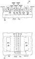
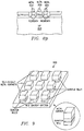
- Figures 4a-b illustrate a first preferred embodiment resonant tunneling diode in cross sectional elevation and plan views.
- Figures 5a-c are band diagrams for the first preferred embodiment diode with various biases.
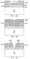
- Figures 6a-k show fabrication steps of the first preferred embodiment method.
- Figures 7a-b illustrate a multiple resonant tunneling preferred embodiment structure.
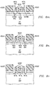
- FIGS 8a-p show fabrication steps of the second preferred embodiment method.
- Figure 9 illustrates in perspective view an array of quantum dots preferred embodiment resonant tunneling structure.
- Figures 10a-c are plan views of steps in fabrication of the array of quantum dots.
- FIGS 11a-f show fabrication steps of another preferred embodiment method.
- Figures 4a-b heuristically show first preferred embodiment resonant tunneling diode, generally denoted by reference numeral 400, in cross sectional elevation and plan views as including gallium arsenide (GaAs) anode 402 with aluminum gallium arsenide (Al X Ga l-X As) cladding 403, AlGaAs tunneling barrier 404, GaAs quantum well 406 with AlGaAs cladding 407, AlGaAs tunneling barrier 408, GaAs cathode 410 with AlGaAs cladding 411, anode metal contact 422, and cathode metal contact 420 all on semi-insulating GaAs substrate 430.
- GaAs gallium arsenide
- Al X Ga l-X As aluminum gallium arsenide
- AlGaAs tunneling barrier 404 AlGaAs tunneling barrier 404
- GaAs quantum well 406 with AlGaAs cladding 407 AlGaAs tunnel
- Tunneling barriers 404/408 are each about 2 nm thick (horizontal direction in Figures 4a-b) and about 20 mm wide (vertical direction in Figure 4b).
- Anode 402 and cathode 410 are about 50 nm thick (vertical direction in Figure 4a) with the AlGaAs claddings 403 and 411 about 100 nm thick on each side of the GaAs.
- Quantum well 406 is about 6 nm long (horizontal in Figure 4a) and 50 nm thick with AlGaAs cladding 407 about 100 nm thick on each side of the GaAs.
- barriers 404/408 primarily impacts the tunneling current magnitude and not the resonance levels which derive from the quantum well dimensions and the barrier heights.
- the GaAs and AlGaAs are doped n-type, and the conduction band discontinuity implies the GaAs (anode, quantum well, and cathode) capture the conduction band electrons from the AlGaAs (modulation doping) leaving a positive charge in the AlGaAs.
- Metal contacts 420 and 422 are about 10 mm by 20 mm (plan view) and connect to the anode and cathode GaAs.
- quantum well 406 as 6 nm by 50 nm implies the edges of the lowest few conduction subbands should be on the order of 100 meV above the conduction band edge due to the two quantized components of crystal momentum in the quantum well.
- the quantum well effectively has a one-dimensional (in the vertical direction in Figure 4b) character and could be termed a quantum wire with the resonant tunneling transversely through the quantum wire.
- FIG. 5a-c represents the band diagram for room temperature electron conduction through diode 400.
- a zero bias produces no current
- a bias of approximately 100 mV across diode 400 yields the first resonant peak current
- a bias of approximately 150 mV across diode 400 leads to the first valley current.
- the majority of the applied bias between anode and cathode appears across the barriers and quantum well.
- Tunneling barriers 404/408 are fabricated by sublithographic trenching followed by AlGaAs regrowth to fill the trenches.
- the AlGaAs of the tunneling barriers may have a composition differing from the AlGaAs cladding the GaAs.
- Figures 6a-d illustrate in cross sectional elevation views a first preferred embodiment method of fabrication of diode 400 which includes the following steps: (1) Begin with four-inch-diameter, semi-insulating GaAs wafer 600 with (100) orientation and 500 mm thickness as the growth substrate. Then grow (such as by metalorganic chemical vapor deposition or molecular beam epitaxy) the epitaxial layers as listed in following Table I; note that AlGaAs denotes Al X Ga l-X As for X a fraction such 0.4, and that silicon provides the n-type doping.
- nitrided wafer 600 into a plasma etcher and anisotropically etch nitride 620 to remove about 80-100 nm. This effectively removes nitride 620 from horizontal areas and leaves only nitride filaments 622 on the vertical sidewalls of the PMMA.
- the etch exposes AlGaAs, but with an etch chemistry of fluoride provides selectivity for nitride over AlGaAs. See Figure 6c. Note that a moderate overetch does not effect the width of the opening and the size of the exposed portion of AlGaAs due to the verticality of the original nitride 620 sidewalls as shown in Figure 6b.
- metal 630-632-634 as the etch mask for an anisotropic plasma etch of AlGaAs and GaAs with chlorine but without BCl3 for breakthrough to limit the erosion of metal ridge 630.
- This forms a trench on each side of metal ridge 630 having a width of 2 nm and a depth of between 130 and 200 nm. See Figure 6j. (9) Insert the wafer into an MBE growth chamber and grow AlGaAs to fill the trench around metal ridge 630; this will form the tunneling barriers, and the portion of GaAs beneath metal ridge 630 will form the quantum well.
- the AlGaAs does not grow on the metal or nitride; see Figure 6k.
- step (9) An alternative which preserves metal ridge 630 follows the same steps up through the AlGaAs regrowth to form the tunneling barriers in step (9) and then repeats the photoresist spin on and partial etchback as in step (7) and Figures 6f-g.
- the thinned metal 632-634 is stripped with a wet etch (or plasma etch) while the remaining photoresist protects metal ridge 630.
- step (10) and strip the nitride and PMMA (plus photoresist) and form ohmic contacts by liftoff.
- a contact to metal ridge 630 may be formed and used to modulate energy levels in the quantum well.
- Figures 7a-b show a preferred embodiment multiple peaked lateral resonant tunneling structure, generally denoted by reference numeral 700, in cross sectional elevation and plan views, respectively, as including InGaAs quantum wells 710, 712, 714 clad with InAlAs, InAlAs tunneling barriers 720, 722, 724, 726 abutting the quantum wells, InGaAs anode 702, InGaAs cathode 704, metal anode contact 732, metal cathode contact 734, InAlAs buffer layer 736, and InP substrate wafer 708.
- the InGaAs heterojunction with AlGaAs has a conduction band discontinuity of about 0.6 eV, so n-type dopants in the InAlAs cladding on the InGaAs modulation dope the InGaAs.
- the multiple quantum wells and barriers implies a multipeaked current-voltage behavior.
- a preferred embodiment method of fabrication of the multiple lateral resonant tunneling essentially follows the method of Figures 6a-k but with a repetition of the metal ridge formation and thereby achieves multiple tunneling barriers.
- the multiple lateral resonant tunneling fabrication method includes the following steps: (1) Begin with four-inch-diameter, semi-insulating InP wafer 800 with (100) orientation and 500 mm thickness.
- the doping level of the n-type InAlAs and InGaAs is roughly 1 x 10¹⁸ atoms/cm3.
- FIG. 8b illustrates the conformal deposition that leaves an depression of width about 20 nm as illustrated.
- the thickness of nitride 820 can be accurately controlled by a slow, low temperature, low pressure deposition, and the nitride thickness determines the width of the depression.
- metal ridges 830-832-834 provide support for the overlying photoresist. If thin ridges of photoresist were to be placed directly on the InAlAs, a problem of sticking to the surface would occur and be exacerbated by the large height-to-width ratio of the ridges. However, metal ridges 830-832-834 stick well to the InAlAs and provide support for the photoresist.
- Figure 9 heuristically illustrates in perspective view an array of quantum dots preferred embodiment, generally denoted by reference numeral 900, as including metal contacts over quantum dots in an array with separation of the dots by tunneling barriers.
- the size of the array can easily be increased by repetition of the fabrication process which resembles the sublithographic line formation of the preceding embodiments.
- Array of quantum dots 900 may be fabricated by essentially two repetitions of the method for fabrication of the multiple resonant tunneling diode. In particular, form three metal ridges as in Figures 8a-n. Then apply another layer of PMMA and e-beam define another 100-nm wide line perpendicular to the line leading to the metal ridges; Figure 10a shows a plan view of a portion showing the exposed InGaAs cladding in the 100 nm wide opening in the PMMA where the opening crosses the three metal ridges.
- Figure 10b is the plan view.
- the preferred embodiments may be altered by omission of the conformal nitride (or other dielectric) layer used to reduce the e-beam defined opening in the PMMA as in Figures 6b-c and 8b-c.
- the opening reduction without conformal dielectric deposition preferred embodiment method proceeds with the following steps: (1) Begin with four-inch-diameter, semi-insulating InP wafer 1100 as the growth substrate. Then grow the undoped epitaxial layers as listed in following Table III; note that InGaAs denotes In X Ga l-X As for X a fraction such 0.4.
- Table III Layer Material Thickness Cladding InP 5 nm Quantum well InGaAs 30 nm Buffer InP 100 nm Substrate InP 500 mm The buffer layer provides a low defect surface for the quantum well growth.
- (2) Spin PMMA onto layered wafer 1100 to a thickness of about 150 nm. Then use an e-beam to expose a minimum linewidth (50 nm wide) line which is 25 mm long in the PMMA; the quantum well will lie along the center of this line. Develop the PMMA; see Figure 11a.
- the etching gas mixture is chlorine plus argon at about equal flows and at a total pressure of about 10 ⁇ 5 Torr. This forms trenches 1141-1142 on each side of metal ridge 1130, each trench having a width of 5 nm and a depth of between 130 and 200 nm.
- the InP and InGaAs may grow as high resistivity polycrystalline on titanium 1130; see Figure 11e which suggests the boundary between epitaxial and polycrystalline growth with a broken line. Alternatively, the InP and InGaAs may not nucleate on the titanium and not grow at all, analogous to Figures 6j-k. MOCVD conditions dictate the growth type.
- the carriers (electrons) in the InGaAs quantum well are provided by modulation doping from the n+ InP and accumulate at the InGaAs-InP interface 1150 adjacent to the n+ InP.
- the InP in the trenches form tunneling barriers for these carriers and the region at the interface between the tunneling barriers forms a quantum wire as previously noted.
- the preferred embodiments may be varied in many ways while retaining one or more of the features of angled deposition for shadowing to define tunneling barrier thicknesses, simultaneous two directional shadowing to define both a quantum well and tunneling barrier lateral dimension, forming multiple adjacent (coupled) resonant tunneling barriers and quantum wells with a single trench etching and refill by repeated angled and conformal depositions to define thicknesses, and forming metal to assist attachment of resist to semiconductor surfaces.
- angles of deposition of the material for creating the overhang could be multiple and varied between (i) close to perpendicular provided no deposition occurs on the semiconductor surface (thus the height-to-width aspect ratio of the opening in the PMMA or resist or nitride filaments determines how close to perpendicular the deposition directions can be) and (ii) close to parallel provided sufficient material can build up to form an overhang.
- the angled depositions could be repeated; for example, with the structure of Figure 8j angled depositions could be used again on the nitride to again define small thicknesses between nitride and vertically deposited metal by overhang.
- the tunneling barriers and quantum well(s) could be varied: the tunneling barriers could be thinner for higher current, the tunneling barriers could be of differing thicknesses, and the quantum well thickness could be varied to adjust the resonant levels up or down.
- the thickness of the tunneling barriers is controlled by the overhang of the angled deposition(s), so a wide range of thicknesses are easily made.
- the materials could be varied such as InAlAs barrier for InGHaAs wells in InP, and so forth.
Landscapes
- Engineering & Computer Science (AREA)
- Chemical & Material Sciences (AREA)
- Nanotechnology (AREA)
- Physics & Mathematics (AREA)
- Mathematical Physics (AREA)
- Theoretical Computer Science (AREA)
- Crystallography & Structural Chemistry (AREA)
- Bipolar Transistors (AREA)
- Semiconductor Lasers (AREA)
- Light Receiving Elements (AREA)
Applications Claiming Priority (2)
| Application Number | Priority Date | Filing Date | Title |
|---|---|---|---|
| US309994 | 1994-09-20 | ||
| US08/309,994 US5529952A (en) | 1994-09-20 | 1994-09-20 | Method of fabricating lateral resonant tunneling structure |
Publications (2)
| Publication Number | Publication Date |
|---|---|
| EP0703626A2 true EP0703626A2 (de) | 1996-03-27 |
| EP0703626A3 EP0703626A3 (de) | 1996-08-07 |
Family
ID=23200543
Family Applications (1)
| Application Number | Title | Priority Date | Filing Date |
|---|---|---|---|
| EP95114532A Withdrawn EP0703626A3 (de) | 1994-09-20 | 1995-09-14 | Struktur mit Resonanztunneleffekt und Herstellungsverfahren |
Country Status (3)
| Country | Link |
|---|---|
| US (1) | US5529952A (de) |
| EP (1) | EP0703626A3 (de) |
| JP (2) | JPH08181335A (de) |
Cited By (7)
| Publication number | Priority date | Publication date | Assignee | Title |
|---|---|---|---|---|
| FR2876498A1 (fr) * | 2004-10-12 | 2006-04-14 | Commissariat Energie Atomique | Procede de realisation d'heterostructures resonnantes a transport planaire |
| WO2007003576A1 (fr) * | 2005-06-30 | 2007-01-11 | Commissariat A L'energie Atomique | Nanostructures a resistance differentielle negative et leur procede de fabrication |
| EP1029359A4 (de) * | 1997-11-10 | 2007-06-06 | Don L Kendall | Quanten-kämme und -spitze |
| FR2896239A1 (fr) * | 2006-01-16 | 2007-07-20 | Commissariat Energie Atomique | Nanostructures a 0, 1, 2 et 3 dimensions, a resistance differentielle negative et procede de fabrication de ces nanostructures |
| EP1507293A4 (de) * | 2002-05-22 | 2008-10-15 | Fujitsu Ltd | Verfahren zur quanten-dot-bildung, quantenhalbleiterbauelement und verfahren zu seiner herstellung |
| CN100449713C (zh) * | 2006-12-14 | 2009-01-07 | 上海交通大学 | 量子逻辑器件的隧穿二极管制备方法 |
| EP1974369A4 (de) * | 2005-12-30 | 2010-11-24 | Chen Chung Chin | Verfahren zur mikrominiaturisierung einer nanostruktur |
Families Citing this family (7)
| Publication number | Priority date | Publication date | Assignee | Title |
|---|---|---|---|---|
| US5654558A (en) * | 1994-11-14 | 1997-08-05 | The United States Of America As Represented By The Secretary Of The Navy | Interband lateral resonant tunneling transistor |
| US6479368B1 (en) | 1998-03-02 | 2002-11-12 | Kabushiki Kaisha Toshiba | Method of manufacturing a semiconductor device having a shallow trench isolating region |
| US6967140B2 (en) * | 2000-03-01 | 2005-11-22 | Intel Corporation | Quantum wire gate device and method of making same |
| US7463661B2 (en) * | 2002-02-27 | 2008-12-09 | National Institute Of Advanced Industrial Science And Technology | Quantum nano-structure semiconductor laser |
| US7138341B1 (en) * | 2004-07-07 | 2006-11-21 | Hewlett-Packard Development Company, L.P. | Process for making a memory structure |
| US10927450B2 (en) * | 2018-12-19 | 2021-02-23 | Applied Materials, Inc. | Methods and apparatus for patterning substrates using asymmetric physical vapor deposition |
| US10927451B2 (en) * | 2019-02-08 | 2021-02-23 | Applied Materials, Inc. | Methods and apparatus for patterning substrates using asymmetric physical vapor deposition |
Family Cites Families (13)
| Publication number | Priority date | Publication date | Assignee | Title |
|---|---|---|---|---|
| JPS5277682A (en) * | 1975-12-24 | 1977-06-30 | Fujitsu Ltd | Manufacture of semiconductor device |
| US4214966A (en) * | 1979-03-20 | 1980-07-29 | Bell Telephone Laboratories, Incorporated | Process useful in the fabrication of articles with metallized surfaces |
| JPS5671981A (en) * | 1979-11-19 | 1981-06-15 | Sumitomo Electric Ind Ltd | Preparation method of semiconductor system |
| US4525919A (en) * | 1982-06-16 | 1985-07-02 | Raytheon Company | Forming sub-micron electrodes by oblique deposition |
| US4599790A (en) * | 1985-01-30 | 1986-07-15 | Texas Instruments Incorporated | Process for forming a T-shaped gate structure |
| US4872947A (en) * | 1986-12-19 | 1989-10-10 | Applied Materials, Inc. | CVD of silicon oxide using TEOS decomposition and in-situ planarization process |
| JPH01241132A (ja) * | 1988-03-23 | 1989-09-26 | Oki Electric Ind Co Ltd | 半導体素子の電極およびその製造方法 |
| JPH022142A (ja) * | 1988-06-13 | 1990-01-08 | Mitsubishi Electric Corp | 電界効果トランジスタ及びその製造方法 |
| US5234848A (en) * | 1991-11-05 | 1993-08-10 | Texas Instruments Incorporated | Method for fabricating lateral resonant tunneling transistor with heterojunction barriers |
| JP3034709B2 (ja) * | 1992-10-20 | 2000-04-17 | 沖電気工業株式会社 | ゲート電極の形成方法 |
| US5346851A (en) * | 1992-11-20 | 1994-09-13 | Texas Instruments Incorporated | Method of fabricating Shannon Cell circuits |
| JPH06244157A (ja) * | 1993-02-12 | 1994-09-02 | Nippon Steel Corp | 半導体装置の製造方法 |
| US5362372A (en) * | 1993-06-11 | 1994-11-08 | Applied Materials, Inc. | Self cleaning collimator |
-
1994
- 1994-09-20 US US08/309,994 patent/US5529952A/en not_active Expired - Lifetime
-
1995
- 1995-09-14 EP EP95114532A patent/EP0703626A3/de not_active Withdrawn
- 1995-09-20 JP JP7241538A patent/JPH08181335A/ja active Pending
-
2007
- 2007-07-25 JP JP2007193482A patent/JP2007324617A/ja not_active Ceased
Cited By (9)
| Publication number | Priority date | Publication date | Assignee | Title |
|---|---|---|---|---|
| EP1029359A4 (de) * | 1997-11-10 | 2007-06-06 | Don L Kendall | Quanten-kämme und -spitze |
| EP1507293A4 (de) * | 2002-05-22 | 2008-10-15 | Fujitsu Ltd | Verfahren zur quanten-dot-bildung, quantenhalbleiterbauelement und verfahren zu seiner herstellung |
| US7755080B2 (en) | 2002-05-22 | 2010-07-13 | Fujitsu Limited | Method for forming quantum dot, and quantum semiconductor device and method for fabricating the same |
| FR2876498A1 (fr) * | 2004-10-12 | 2006-04-14 | Commissariat Energie Atomique | Procede de realisation d'heterostructures resonnantes a transport planaire |
| US8193525B2 (en) | 2004-10-12 | 2012-06-05 | Commissariat A L'energie Atomique | Method for producing planar transporting resonance heterostructures |
| WO2007003576A1 (fr) * | 2005-06-30 | 2007-01-11 | Commissariat A L'energie Atomique | Nanostructures a resistance differentielle negative et leur procede de fabrication |
| EP1974369A4 (de) * | 2005-12-30 | 2010-11-24 | Chen Chung Chin | Verfahren zur mikrominiaturisierung einer nanostruktur |
| FR2896239A1 (fr) * | 2006-01-16 | 2007-07-20 | Commissariat Energie Atomique | Nanostructures a 0, 1, 2 et 3 dimensions, a resistance differentielle negative et procede de fabrication de ces nanostructures |
| CN100449713C (zh) * | 2006-12-14 | 2009-01-07 | 上海交通大学 | 量子逻辑器件的隧穿二极管制备方法 |
Also Published As
| Publication number | Publication date |
|---|---|
| EP0703626A3 (de) | 1996-08-07 |
| JPH08181335A (ja) | 1996-07-12 |
| JP2007324617A (ja) | 2007-12-13 |
| US5529952A (en) | 1996-06-25 |
Similar Documents
| Publication | Publication Date | Title |
|---|---|---|
| US5593908A (en) | Lateral resonant tunneling | |
| JP2007324617A (ja) | 横方向共振トンネリング | |
| US7247891B2 (en) | Semiconductor device and method for fabricating the same | |
| JP3319472B2 (ja) | 半導体装置とその製造方法 | |
| EP1109226A2 (de) | Halbleiteranordnung und Verfahren zu ihrer Herstellung, das das Niederfrequenzgeräusch vermindert | |
| US5283448A (en) | MESFET with indium gallium arsenide etch stop | |
| US4751195A (en) | Method of manufacturing a heterojunction bipolar transistor | |
| EP0478923B1 (de) | Verfahren zum Herstellen selbst-ausrichtender bipolarer Transistoren mit Heteroübergang | |
| EP0855748B1 (de) | Heteroübergangsfeldeffekttransistor und Verfahren zu dessen Herstellung | |
| EP0656646A1 (de) | Herstellungsverfahren von Vorrichtungen mit vergrabenen Schichten durch epitaxiales Wachstum | |
| US4868633A (en) | Selective epitaxy devices and method | |
| EP0507434A2 (de) | Verfahren zur Herstellung von Halbleietervorrichtungen | |
| US5013682A (en) | Method for selective epitaxy using a WSI mask | |
| JP4465890B2 (ja) | 半導体装置の製造方法 | |
| CN114883192B (zh) | 绝缘衬底上硅与iii-v族器件的单片异质集成结构及制备方法 | |
| US5471078A (en) | Self-aligned heterojunction bipolar transistor | |
| US6828603B2 (en) | Hetero-bipolar transistor with a sub-collector layer having a first portion and plural second portions | |
| JP4026347B2 (ja) | 化合物半導体バイポーラトランジスタの製造方法 | |
| US5629215A (en) | Method of fabricating and contacting ultra-small three terminal semiconductor devices | |
| JP3747391B2 (ja) | 化合物半導体装置及びその製造方法 | |
| JP2003045898A (ja) | 半導体装置およびその製造方法 | |
| JP2658513B2 (ja) | 電界効果トランジスタ | |
| EP0786147A2 (de) | Laser mit streifenform in einem kanal | |
| JP2924007B2 (ja) | 化合物半導体装置及びその製造方法 | |
| JP3225902B2 (ja) | 半導体装置の製造方法 |
Legal Events
| Date | Code | Title | Description |
|---|---|---|---|
| PUAI | Public reference made under article 153(3) epc to a published international application that has entered the european phase |
Free format text: ORIGINAL CODE: 0009012 |
|
| AK | Designated contracting states |
Kind code of ref document: A2 Designated state(s): DE FR GB IT NL |
|
| PUAL | Search report despatched |
Free format text: ORIGINAL CODE: 0009013 |
|
| AK | Designated contracting states |
Kind code of ref document: A3 Designated state(s): DE FR GB IT NL |
|
| 17P | Request for examination filed |
Effective date: 19970207 |
|
| 17Q | First examination report despatched |
Effective date: 19980702 |
|
| STAA | Information on the status of an ep patent application or granted ep patent |
Free format text: STATUS: THE APPLICATION IS DEEMED TO BE WITHDRAWN |
|
| 18D | Application deemed to be withdrawn |
Effective date: 20000216 |