EP0703634A1 - Cavite resonante et filtre utilisant cet element - Google Patents
Cavite resonante et filtre utilisant cet element Download PDFInfo
- Publication number
- EP0703634A1 EP0703634A1 EP95913401A EP95913401A EP0703634A1 EP 0703634 A1 EP0703634 A1 EP 0703634A1 EP 95913401 A EP95913401 A EP 95913401A EP 95913401 A EP95913401 A EP 95913401A EP 0703634 A1 EP0703634 A1 EP 0703634A1
- Authority
- EP
- European Patent Office
- Prior art keywords
- external conductor
- fixed electrode
- electrode
- fixed
- input terminal
- Prior art date
- Legal status (The legal status is an assumption and is not a legal conclusion. Google has not performed a legal analysis and makes no representation as to the accuracy of the status listed.)
- Granted
Links
Images

























Classifications
-
- H—ELECTRICITY
- H01—ELECTRIC ELEMENTS
- H01P—WAVEGUIDES; RESONATORS, LINES, OR OTHER DEVICES OF THE WAVEGUIDE TYPE
- H01P1/00—Auxiliary devices
- H01P1/20—Frequency-selective devices, e.g. filters
-
- H—ELECTRICITY
- H01—ELECTRIC ELEMENTS
- H01P—WAVEGUIDES; RESONATORS, LINES, OR OTHER DEVICES OF THE WAVEGUIDE TYPE
- H01P1/00—Auxiliary devices
- H01P1/20—Frequency-selective devices, e.g. filters
- H01P1/201—Filters for transverse electromagnetic waves
- H01P1/205—Comb or interdigital filters; Cascaded coaxial cavities
-
- H—ELECTRICITY
- H01—ELECTRIC ELEMENTS
- H01P—WAVEGUIDES; RESONATORS, LINES, OR OTHER DEVICES OF THE WAVEGUIDE TYPE
- H01P1/00—Auxiliary devices
- H01P1/20—Frequency-selective devices, e.g. filters
- H01P1/207—Hollow waveguide filters
- H01P1/208—Cascaded cavities; Cascaded resonators inside a hollow waveguide structure
-
- H—ELECTRICITY
- H01—ELECTRIC ELEMENTS
- H01P—WAVEGUIDES; RESONATORS, LINES, OR OTHER DEVICES OF THE WAVEGUIDE TYPE
- H01P7/00—Resonators of the waveguide type
-
- H—ELECTRICITY
- H01—ELECTRIC ELEMENTS
- H01P—WAVEGUIDES; RESONATORS, LINES, OR OTHER DEVICES OF THE WAVEGUIDE TYPE
- H01P7/00—Resonators of the waveguide type
- H01P7/04—Coaxial resonators
-
- H—ELECTRICITY
- H01—ELECTRIC ELEMENTS
- H01P—WAVEGUIDES; RESONATORS, LINES, OR OTHER DEVICES OF THE WAVEGUIDE TYPE
- H01P7/00—Resonators of the waveguide type
- H01P7/06—Cavity resonators
Definitions
- the present invneiton relates to a resonator that is used for the elimination of noise, the splitting and synthesis of signals, etc., in radio communication devices, broadcast devices, and so on, and also relates to a filter comprising this resonator.
- Resonators composed of capacitors and coils which are lumped-parameter circuit elements, or helical resonators have been conventionally used in relatively low frequency bands, such as short wave and ultrashort wave bands.
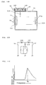
- Fig. 1 is a vertical cross section of a conventional helical resonator
- Fig. 2 is a horizontal cross section thereof.
- This helical resonator comprises an external conductor 201 ; a capacity formation electrode 203 ; insulators 2041 and 2042 ; a helical resonance element 202 at one end mechanically fixed to and electrically connected with the inside wall of the external conductor 201 , wound coil-like in its middle portion, attached at the other end to the capacity formation electrode 203 , and fixed to the inside wall of the external conductor 201 via the insulators 2041 and 2042 ; a movable electrode 205 ; a drive screw 206 to one end of which the movable electrode 205 is attached, and which passes through the external conductor 201 ; a lock nut 207 that is used to fix the drive screw 206 to the external conductor 201 ; and input/output coupling elements and input/output terminals (not shown).
- the resonance frequency can be finely tuned by rotating the drive screw 206 forward or backward to move the movable electrode 205 ahead or back so that the capacity of the electrode 203 can be varied.
- the conventional resonator described above has the following drawbacks.
- the helical resonance element 202 is formed by the winding of a metallic wire or a relatively thin rod-shaped conductor in the form of a coil, not only is the heat-radiating surface area of the helical resonance element 202 itself small, but the thermal conductivity into the external conductor 201 is poor, so the heat produced by power loss in the helical resonance element 202 is not effectively radiated from the helical resonance element 202 and the external conductor 201 , and the resonance frequency fluctuates as a result of distortion due to the elevated temperature of the various constituent components of the resonator.
- the ends of the helical resonance element 202 are directly or indirectly supported by and fixed to the inside wall of the external conductor 201 , but the middle portion is not supported by any support, and is instead formed so that it maintains a coiled posture by its own rigidity, so vibration resistance is poor, fabrication is difficult, and the cost is high.
- a helical resonance element Because of its high impedance, a helical resonance element has inferior withstand voltage characteristics.
- a resonator comprises: an external conductor; a resonance capacity element comprising a dielectric plate fixed at the upper and lower ends to the upper and lower walls, respectively, of the external conductor, and electrodes made of a metal plate or a metal thin layer provided on the front and back sides of the dielectric plate, wherein the lower end of one of the electrodes is electrically connected to the lower wall of the external conductor, and a gap is formed between the upper end of the electrode and the upper wall of the external conductor, while the upper end of the other electrode is electrically connected to the upper wall of the external conductor, and a gap is formed between the lower end of the other electrode and the lower wall of the external conductor; an input terminal; an output terminal; and means for connecting one of the electrodes of the resonance capacity element to the input terminal and the output terminal in a high-frequency fashion.
- Another resonator comprises: an external conductor; a resonance capacity element comprising a dielectric plate fixed at the upper and lower ends to the upper and lower walls, respectively, of the external conductor, and electrodes made of a metal plate or a metal thin layer provided on the front and back sides of the dielectric plate, wherein the lower end of one of the electrodes is electrically connected to the lower wall of the external conductor, and a gap is formed between the upper end of said one electrode and the upper wall of the external conductor, while the upper end of the other electrode is electrically connected to the upper wall of the external conductor, and a gap is formed between the lower end of said other electrode and the lower wall of the external conductor; an input terminal; an output terminal; two inductance elements or two capacity elements for the compensation of transmission characteristics connected in series between the input terminal and the output terminal; and means for connecting one of the electrodes of the resonance capacity element to the connection point of the two inductance elements or the two capacity elements in a high-frequency fashion.
- a filter according to the present invention comprises: a common external conductor; a plurality of resonance capacity elements connected in series in a high-frequency fashion and comprising a plurality of dielectric plates provided at suitable intervals in the external conductor and fixed at the upper and lower ends to the upper and lower walls, respectively, of the external conductor, and electrodes made of a metal plate or a metal thin layer provided on the front and back sides of each dielectric plate, wherein the lower end of one of the electrodes is electrically connected to the lower wall of the external conductor, and a gap is formed between the upper end of said one electrode and the upper wall of the external conductor, while the upper end of the other electrode is electrically connected to the upper wall of the external conductor, and a gap is formed between the lower end of the other electrode and the lower wall of the external conductor; an input terminal; an output terminal; means for connecting one of the electrodes of the top resonance capacity element of the plurality of resonance capacity elements to the input terminal in a high-frequency fashion; and means for connecting one of the electrodes of the
- Another resonator comprises: an external conductor; a variable resonance capacity element comprising a hollow cylinder composed of a solid dielectric whose lower end portion is fixed to the lower wall of said external conductor and whose upper end portion faces the upper wall of the external conductor a suitable distance away, a fixed electrode composed of a metal thin layer that adheres around the outer surface of the hollow cylinder and whose lower end portion is electrically connected to the lower wall of the external conductor, and a hollow or solid cylindrical movable electrode that is coaxial with the fixed electrode and is attached to the upper wall of the external conductor so that the insertion length of the movable electrode into the hollow cylinder can be varied; an input terminal; an output terminal; and means for connecting the fixed electrode to the input terminal and the output terminal in a high-frequency fashion.
- Another resonator comprises : an external conductor; a variable resonance capacity element comprising a hollow cylinder composed of a solid dielectric whose lower end portion is fixed to the lower wall of the external conductor and whose upper end portion faces the upper wall of the external conductor a suitable distance away, a fixed electrode composed of a metal thin layer that adheres around the outer surface of the hollow cylinder and whose lower end portion is electrically connected to the lower wall of the external conductor, and a hollow or solid cylindrical movable electrode that is coaxial with the fixed electrode and is attached to the upper wall of the external conductor so that the insertion length of the movable elctrode into the hollow cylinder can be varied; an input terminal; an output terminal; two inductance elements or two capacity elements for the compensation of transmission characteristics connected in series between the input terminal and the output terminal; and means for connecting the fixed electrode to the connecting point of the two inductance elements or the two capacity elements in a high-frequency fashion.
- Another filter according the present invention comprises: an external conductor; a plurality of variable resonance capacity elements connected in series in a high-frequency fashion and comprising a plurality of hollow cylinders provided at suitable intervals and composed of a solid dielectric whose lower end portion is fixed to the lower wall of the external conductor and whose upper end portion faces the upper wall of the external conductor a suitable distance away, a fixed electrode composed of a metal thin layer that is provided on each of the hollow cylinder, adheres around the outer surface of the hollow cylinders, and whose lower end portion is electrically connected to the lower wall of the external conductor, and a hollow or solid cylindrical movable electrode that is coaxial with the fixed electrode and is attached to the upper wall of the external conductor so that the insertion length of the movable electrode into the hollow cylinder can be varied; an input terminal; an output terminal; means for connecting the top resonance capacity element of the plurality of resonance capacity elements to the input terminal in a high-frequency fashion; and means for connecting the last resonance capacity element of the plurality of resonance capacity elements
- a resonator comprises: an external conductor; a variable resonance capacity element comprising of a fixed electrode composed of a hollow cylindrical conductor whose lower end portion is fixed to the lower wall of the external conductor and whose upper end portion faces the upper wall of the external conductor a suitable distance away and a movable electrode composed of a hollow or solid cylindrical conductor that is coaxial with the fixed electrode and is attached to the upper wall of the external conductor so that the insertion length of the movable electrode into the fixed electrode can be varied; an input terminal; an output terminal; and means for connecting the fixed electrode to the input terminal and the output terminal in a high-frequency fashion.
- Another filter according to the present invention comprises: an external conductor; a plurality of variable resonance capacity elements connected in series in a high-frequency fashion, provided at suitable intervals, and comprising of a fixed electrode composed of a hollow cylindrical conductor whose lower end portion is fixed to the lower wall of the external conductor and whose upper end portion faces the upper wall of the external conductor a suitable distance away and a movable electrode composed of a hollow or solid cylindrical conductor that is coaxial with the fixed electrode and is attached to the upper wall of the external conductor so that the insertion length of the movable electrode into the fixed electrode can be varied; an input terminal; an output terminal; means for connecting the fixed electrode of the top resonance capacity element of the plurality of resonance capacity elements to the input terminal in a high-frequency fashion; and means for connecting the fixed electrode of the last resonance capacity element of the plurality of resonance capacity elements to the output terminal in a high-frequency fashion.
- Another resonator comprises: an external conductor; a variable resonance capacity element comprising a hollow cylinder composed of a solid dielectric whose upper and lower end portions face the upper and lower walls, respectively, of the external conductor a suitable distance away, first fixed electrode composed of a metal thin layer that adheres around the inner surface of the hollow cylinder and whose lower end portion is electrically connected to the lower wall of the external conductor, a second fixed electrode composed of a metal thin layer that adheres around the outer surface of hollow cylinder and whose upper end portion is electrically connected to the upper wall of the external conductor, and a hollow or solid cylindrical movable electrode that is coaxial with the first and second fixed electrodes and is attached to the upper wall of the external conductor so that the insertion length into the above-mentioned hollow cylinder can be varied; an input terminal; an output terminal; and means for connecting the second fixed electrode to the input terminal and the output terminal in a high-frequency fashion.
- Another resonator comprises: an external conductor; a variable resonance capacity element comprising a hollow cylinder composed of a solid dielectric whose upper and lower end portions face the upper and lower walls, respectively, of the external conductor a suitable distance away, a first fixed electrode composed of a metal thin layer that adheres around the inner surface of the hollow cylinder and whose lower end portion is electrically connected to the lower wall of the external conductor, a second fixed electrode composed of a metal thin layer that adheres around the outer surface of the hollow cylinder and whose upper end portion is electrically connected to the upper wall of the external conductor, and a hollow or solid cylindrical movable electrode that is coaxial with the first and second fixed electrodes and is attached to the upper wall of the external conductor so that the insertion length of the movable electrode into the hollow cylinder can be varied; an input terminal; an output terminal; two inductance elements or two capacity elements for the compensation of transmission characteristics connected in series between the input terminal and the output terminal; and means for connecting the second fixed electrode to the connecting point
- Another filter according to the present invention comprises: a common external conductor; a plurality of variable resonance capacity elements connected in series in a high-frequency fashion and comprising a hollow cylinder composed of a solid dielectric whose upper and lower end portions face the upper and lower walls, respectively, of the external conductor a suitable distance away, a first fixed electrode composed of a metal thin layer that adheres around the inner surface of the said hollow cylinder and whose lower end portion is electrically connected to the lower wall of the external conductor, a second fixed electrode composed of a metal thin layer that adheres around the outer surface of the hollow cylinder and whose upper end portion is electrically connected to the upper wall of the external conductor, and a hollow or solid cylindrical movable electrode that is coaxial with the first and second fixed electrodes and is attached to the upper wall of the external conductor so that the insertion length of the movable electrode into the hollow cylinder can be varied; an input terminal; an output terminal; and means for connecting the second fixed electrode of the top resonance capacity element of the plurality of resonance capacity elements to the
- Another resonator comprises: an external conductor; a variable resonance capacity element comprising a first fixed electrode composed of a metal hollow cylinder whose lower end portion is fixed to the lower wall of the external conductor, a second fixed electrode composed of a metal hollow cylinder that is provided coaxially with the first fixed electrode with a gap on the outside of the first fixed electrode, and whose upper end portion is fixed to the upper wall of the external conductor, and a hollow or solid cylindrical movable electrode that is coaxial with the first and second fixed electrodes and is attached to the upper wall of the external conductor so that the insertion length of the movabe electrode into the first fixed electrode can be varied; an input terminal; an output terminal; and means for connecting the second fixed electrode to the input terminal and the output terminal in a high-frequency fashion.
- Another resonator comprises: an external conductor; a variable resonance capacity element comprising a first fixed electrode composed of a metal hollow cylinder whose lower end portion is fixed to the lower wall of the external conductor, a second fixed electrode composed of a metal hollow cylinder that is provided coaxially with the first fixed electrode with a gap on the outside of said first fixed electrode, and whose upper end portion is fixed to the upper wall of the external conductor, and a hollow or solid cylindrical movable electrode that is coaxial with the first and second fixed electrodes and is attached to the upper wall of the external conductor so that the insertion length of the movable electrode into the first fixed electrode can be varied; an input terminal; an output terminal; two inductance elements or two capacity elements for the compensation of transmission characteristics connected in series between the input terminal and the output terminal; and means for connecting the second fixed electrode to the connection point of the two inductance elements or the two capacity elements in a high-frequency fashion.
- Another filter according to the present invention comprises: a common external conductor; a plurality of variable resonance capacity elements connected in series in a high-frequency fashion, provided at suitable intervals and comprising a first fixed electrode composed of a metal hollow cylinder whose lower end portion is fixed to the lower wall of the external conductor, a second fixed electrode composed of a metal hollow cylinder that is provided coaxially with the first fixed electrode with a gap on the outside of the first fixed electrode, and whose upper end portion is fixed to the upper wall of the external conductor, and a hollow or solid cylindrical movable electrode that is coaxial with the first and second fixed electrodes and is attached to the upper wall of the external conductor so that the insertion length of the movable electrode into the first fixed electrode can be varied; an input terminal; an output terminal; means for connecting the second fixed electrode of the top resonance capacity element of the plurality of resonance capacity elements to the input terminal in a high-frequency fashion; and means for connecting the second fixed electrode of the last resonance capacity element of the plurality of resonance capacity elements to the output terminal in
- the resonator according to the present invention has good thermal conductivity between the resonance capacity element and the external conductor because of the relatively large thermal radiation surface area of the resonance capacity element, so heat is effectively radiated from the resonance capacity element and the external conductor, and therefore the rise in the temperature of the various resonator components is kept low and there is extremely little fluctuation in resonance frequency caused by distortion of the components as a result of elevated temperature. Furthermore, the structure is extremely simple and mechanically tough, so the product has excellent vibration resistance. The withstand voltage characteristics are also good because of the low impedance of the resonator.
- the range over which the capacity can be varied is wider and the resonance frequency can be set over a wider range, so resonators with a greater variety of resonance frequencies can be formed using parts of the same configurations and the same dimensions, and the costs entailed can therefore be lowered.
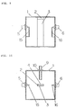
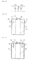
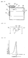
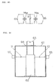
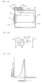
- Fig. 3 is a vertical cross section of the resonator of the first embodiment according to the present invention
- Fig. 4 is a horizontal cross section thereof
- Fig. 5 is a vertical cross section rotated 90° from Fig. 3.
- the resonator of this embodiemnt comprises a cubic external conductor 1 , a slender ribbon-shaped dielectric plate 2 , capacity formation electrodes 3 and 4 , an input terminal 5 , an output terminal 6 , an input coupling wire 7 , an output coupling wire 8 , a resonance frequency fine-tuning element 9 , and a lock nut 10 that is used to fix the fine-turning element 9 .
- the external conductor 1 may also be a bottomed cylinder.
- the upper and lower ends of the dielectric plate 2 are fixed by an adhesive agent or other suitable means to the upper and lower walls, respectively, of the external conductor 1 .
- the capacity formation electrodes 3 and 4 are made of metal thin layers bonded to the front and back of the dielectric plate 2 , or of metal plates applied to the front and back of the dielectric plate 2 . As shown in Fig. 5, regardless of whether the capacity formation electrodes 3 and 4 are made of a metal thin layer or a metal plate, the lower end of one of the electrodes (in this case the capacity formation electrode 3 ) is electrically connected to the lower wall of the external conductor 1 , and a gap of suitable width is provided between the upper end of the capacity formation electrode 3 and the upper wall of the external conductor 1 so that both may not be electrically connected each other.
- the upper end of the capacity formation electrode 4 is electrically connected to the upper wall of the external conductor 1 , and a gap of suitable width is provided between the lower end of the capacity formation electrode 4 and the lower wall of the external conductor 1 so that both may not be electrically connected each other.
- the input terminal 5 and the output terminal 6 both consist of coaxial plugs, for example, and the external conductor that forms each coaxial plug is connected to the external conductor 1 .
- One end of the input coupling wire 7 is connected to the internal conductor of the input terminal 5 , and the other end is connected to the capacity formation electrode 3 .
- One end of the output coupling wire 8 is connected to the internal conductor of the output terminal 6 , and the other end is connected to the capacity formation electrode 3 .
- the fine-tuning element 9 is in this case made of a metal screw threaded into the wall of the external conductor 1 .
- a parallel resonance circuit whose equivalent circuit is shown in Fig. 6, is composed of the distributed inductance resulting from the external conductor 1 and the capacity of the resonance capacity element formed by the dielectric plate 2 and the capacity formation electrodes 3 and 4 .
- a symbol R represents the resonance circuit
- a symbol M 5R represents the input magnetic field coupling coefficient
- a symbol M R6 represents the output magnetic field coupling coefficient.
- the electromagnetic field distribution in this resonator becomes as shown in Figs. 4 and 5.
- the broken line H marked with arrows in Fig. 4 represents the magnetic field
- the solid arrowed line E in Fig. 5 represents the electric field vector
- the solid arrowed line I represents the current.
- this resonator is a low impedance type with good withstand voltage characteristics.
- the Q (Q d ) of the resonance capacity element consisting of the dielectric plate 2 and the capacity formation electrodes 3 and 4 can be ignored. Since the electromagnetic energy that can be accumulated in this resonator will correspond to the volume of the external conductor 1 , and the resistance in the metal portion of this resonator can be kept extremely low, an extremely large unloaded Q can be obtained.
- the magnitude of the unloaded Q (Q u ) when the external conductor 1 and the capacity formation electrodes 3 and 4 are made of copper in this resonator will vary with the ratio of the inductance to the capacity in the resonator.
- the inventor was able to obtain the following experimental equation for unloaded Q (Q u ) through the use of prototypes.
- tap coupling with the coupling wires 7 and 8 was given as an example of means for coupling in a high-frequency fashion the input terminal 5 with the capacity formation electrode 3 , and the output terminal 6 with the capacity formation electrode 3 .
- means for capacitively coupling the input terminal 5 with the capacity formation electrode 3 via the capacity element 11 and means for capacitively coupling the output terminal 6 with the capacity formation 3 via the capacity element 12 may also be used, as shown in Fig. 7.
- probes 13 and 14 may be used as the input/output coupling means, as shown in Fig. 8.
- Loops 15 and 16 may also be used as the input/output coupling means, as shown in Figs. 9 and 10 which are the vertical cross section and the horizontal cross section, respectively, of the resonator.
- the capacity formation electrode 3 that forms the resonance capacity element is coupled in high-frequency fashion to the input terminal 5 and the output terminal 6 .
- the present invention can also be implemented with a structure in which the capacity formation electrode 4 is coupled in high-frequency fashion to the input terminal 5 and the output terminal 6 .
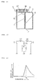
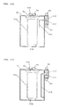
- Fig. 11 is a vertical cross section of the resonator of the second embodiment according to the present invention
- Fig. 12 is an equivalent circuit diagram thereof
- Fig. 13 is a diagram illustrating the transmission characteristics thereof.
- a low-pass filter circuit is composed of inductance elements 17 and 18 for the compensation of transmission characteristics, interposed between the connection terminals 5 and 6 for an external circuit, and a capacity element 19 connected between the capacity formation electrode 3 and the connection point of the inductance elements 17 and 18 .
- the slope of the attenuation characteristic curve in the frequency region lower than the resonance frequency f0 is steep, while the slope of the attenuation characteristic curve in the frequency region higher than the resonance frequency f0 is gentle, and a transmission inhibition band is formed in the frequency region including the resonance frequency f0.
- the resonance frequency f0 of the circuit composed of the resonance circuit R and the coupling-use capacity element 19 changes according to the capacity of the coupling-use capacity element 19 .
- the fine tuning of the resonance frequency can also be performed by the provision of an adjustment element simlilar to the resonance frequency fine-tuning element 9 , as shown in Fig. 4.
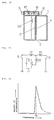
- Fig. 14 is a vertical cross section of the resonator of the third embodiment according to the present invention
- Fig. 15 is an equivalent circuit diagram thereof
- Fig. 16 is a diagram illustrating the transmission characteristics thereof.
- This embodiment differs from the second embodiment shown in Fig. 11 in that the coupling of the connection point of the inductance elements 17 and 18 with the capacity formation electrode is performed by tap coupling using an inductance element 20 , and in that the resonance frequency f0 of the circuit composed of the resonance circuit R and the coupling-use inductance element 20 changes according to the inductance of the inductance element 20 .
- the rest of the structure and operation is substantially the same as in the second embodiment shown in Fig. 11.
- Fig. 17 is a vertical cross section of the resonator of the fourth embodiment according to the present invention
- Fig. 18 is an equivalent circuit diagram thereof
- Fig. 19 is a diagram illustrating the transmission characteristics thereof.
- This embodiment differs from the second embodiment shown in Fig. 11 in that the inductance elements 17 and 18 in the second embodiment shown in Fig. 11 are replaced with capacity elements 21 and 22 .
- the rest of the structure is the same as in the second shown in Fig. 11.
- the slope of the attenuation characteristic curve in the frequency region lower than the resonance frequency f0 is gentle, while the slope of the attenuation characteristic curve in the frequency region higher than the resonance frequency f0 is steep, and a transmission inhibition band is formed in the frequency region including the resonance frequency f0.
- Fig. 20 is a vertical cross section of the resonator of the fifth embodiment according to the present invention
- Fig. 21 is an equivalent circuit diagram thereof
- Fig. 22 is a diagram illustrating the transmission characteristics thereof.
- This embodiment is the same as the fourth embodiment shown in Fig. 17 in that the capacity elements 21 and 22 are used as transmission characteristic compensation elements, and is the same as the embodiment shown in Fig. 14 in that tap coupling is performed using the inductance element 20 .
- the rest of the structure is the same as in the fourth embodiment shown in Fig. 17.
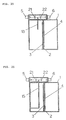
- Figs. 23, 24, 25, and 26 are vertical cross sections of the sixth, seventh, eighth, and ninth embodiments of the present invention, respectively.
- the resonator shown in Fig. 23 has a probe 13 in place of the coupling element 19 of the second embodiment shown in Fig. 11; the resonator shown in Fig. 24 has a loop 15 in place of the coupling element 19 of the second embodiment shown in Fig. 11; the resonator shown in Fig. 25 has a probe 13 in place of the coupling element 19 of the fourth embodiment shown in Fig. 17; and the resonator shown in Fig. 26 has a loop 15 in place of the coupling element 19 of the fourth embodiment shown in Fig. 17.
- the rest of the structure in the respective Figs. is the same as the structure in Figs. 11 or 17.
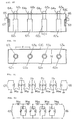
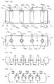
- Fig. 27 is a cross section of a filter constructed using a plurality of the resonators shown in Fig. 11.
- This filter comprises an external conductor 1C , partition walls 1S1 , 1S2 , and 1S3 , resonance capacity elements CE1 , CE2 , CE3 , and CE4 , external circuit connection terminals 5 and 6 , inductance elements 171 , 181 , 172 , 182 , 173 , 183 , 174 , and 184 for the compensation of transmission characteristics, and coupling capacity elements 191 , 192 , 193, and 194 .
- the resonance capacity elements CE1 through CE4 have the same structure as the resonance capacity element shown in Fig. 3. Specifically, electrodes made of a metal thin plate or a metal plate are provided on the front and back sides of a dielectric plate whose upper and lower ends are fixed to the upper and lower walls, respectively, of a common external conductor IC , the lower end of one of the electrodes is electrically connected to the lower wall of the common external conductor IC , and a gap is formed between the upper end of said one electrode and the upper wall of the common external conductor IC , while the upper end of the other electrode is electrically connected to the upper wall of the external conductor IC , and a gap is formed between the lower end of the other electrode and the lower wall of the external conductor IC .
- Fig. 28 is an equivalent circuit diagram of the filter shown in Fig. 27.
- Symbols R1 through R4 represent resonance circuits composed of the common external conductor IC and the resonance capacity elements CE1 through CE4 ;
- reference numerals 171 , 1871 through 1873 , and 184 represent inductance elements for the compensation of transmission characteristics;
- the reference numeral 1871 represents a synthetic inductance element of the inductance elements 181 and 172 in Fig. 27;
- the reference numeral 1872 represents a synthetic inductance element of the inductance elements 182 and 173 ;
- the reference numeral 1873 represents a synthetic inductance element of the inductance elements 183 and 174 ;
- reference numerals 191 through 194 represent coupling capacity elements.
- the transmission characteristic of the filter shown in Fig. 27 is the superimposition of the transmission characteristics of the resonators at all stages composing this filter, that is, the superimposition of the transmission characteristics substantially the same as the transmission characteristics shown in Fig. 13.
- the resonance frequencies (f0 in Fig. 13) of all stages composed of a resonator and a coupling-use capacity element are represented by f01 through f04, respectively. Suitable adjustment of these resonance frequencies such that they approach each other, for instance, allows a region of inhibition with a large amount of attenuation to be realized, while adjustment of these resonance frequencies f01 through f04 to adequately separated values allows a region of inhibition with a wide range of frequency to be realized.
- Fig. 29 is an equivalent circuit diagram of a filter constructed using a plurality of the resonators shown in Fig. 14.
- the reference numerals 201 through 204 represent coupling-use inductance elements (tap coupling), and the rest of the symbols are the same as in Fig. 24.
- the transmission characteristics of this filter represented by the equivalent circuit shown in Fig. 29, is the superimposition of the transmission characteristics of the resonators at all stages composing this filter, that is, the superimposition of the transmission characteristics substantially the same as the transmission characteristics shown in Fig. 16. Suitable adjustment of each resonance frequency allows the frequency range and the amount of attenuation in the synthesis inhibition region to be suitably adjusted.
- Fig. 30 is a vertical cross section of a filter constructed using the resonator shown in Fig. 20.
- This filter comprises an external conductor 1C , partition walls 1S1 , 1S2 , and 1S3 , resonance capacity elements CE1 , CE2 , CE3 , and CE4 , external circuit connection terminals 5 and 6 , inductance elements 211 , 221 , 212 , 222 , 213 , 223 , 214 , and 224 for the compensation of transmission characteristics, and inductance elements 201 , 202 , 203 , and 204 for the tap coupling.
- Fig. 31 is an equivalent circuit diagram of the filter shown in Fig. 30.
- Symbols R1 through R4 represent resonance circuits
- reference numerals 211 , 2211 through 2213 , and 224 represent capacity elements for the compensation of transmission characteristics
- the reference numerals 2211 represents a synthetic capacity element of the capacity elements 221 and 212 in Fig. 26
- the reference numeral 2212 represents a synthetic capacity element of the capacity elements 222 and 213
- the reference numeral 2213 represents a synthetic capacity element of the capacity elements 223 and 214
- reference numerals 201 through 204 represent inductance elements for tap coupling.
- the transmission characteristics of the filter shown in Fig. 30 is the superimposition of the transmission characteristics of the resonators at all stages composing this filter, that is, the superimposition of the transmission characteristics substantially the same as the transmission characteristics shown in Fig. 22. Suitable adjustment of these resonance frequencies allows the frequency range and the amount of attenuation in the synthesis inhibition region to be suitably adjusted.
- Fig. 32 is an equivalent circuit diagram of a filter constructed using the resonator shown in Fig. 17.
- Reference numerals 191 through 194 represent coupling-use capacity elements, and the rest of the symbols are the same as in Fig. 31.
- the transmission characteristics of this filter expressed by the equivalent circuit shown in Fig. 32 is the superimposition of the transmission characteristics of the resonators at all stages composing this filter, that is, the superimposition of the transmission characteristics substantially the same as the transmission characteristics shown in Fig. 19. Suitable adjustment of these resonance frequencies allows the frequency range and the amount of attenuation in the synthesis inhibition region to be suitably adjusted.
- Figs. 27 through 32 illustrate examples in which four resonance capacity elements are provided, that is, when the order n of the circuit is 4, the present invention can also be implemented when order of the circuit is suitably increased or decreased.
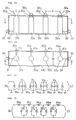
- Fig. 33 is a vertical cross section of a filter constructed using the resonator shown in Fig. 3, and Fig. 34 is a horizontal cross section thereof.
- This filter comprises an external conductor 1C , resonance capacity elements CE1 , CE2 , CE3 , and CE4 having the same structure as that described for Fig. 23, an input terminal 5 , an output terminal 6 , an input coupling wire 7 , an output coupling wire 8 , resonance frequency fine-tuning elements 91 , 92 , 93 , and 94 , and lock nuts 101 , 102 , 103 , and 104 that is used to fix the fine-tuning elements 91 , 92 , 93 , and 94 .
- Fig. 35 is an equivalent circuit diagram of the filter shown in Figs. 33 and 34.
- Symbols R1 through R4 represent resonance circuits
- the symbol M51 represents the input magnetic field coupling coefficient
- the symbol M46 represents the output magnetic field coupling coefficient
- symbols M12 through M34 represent interstage magnetic field coupling coefficients.
- Fig. 36 is a converted equivalent circuit diagram of the equivalent circuit diagram shown in Fig. 35. The symbols are the same as in Fig. 35.
- Figs. 33 through 36 illustrate examples in which the order n of the circuit is 4, the present invention can also be implemented when the order of the circuit is suitably increased or decreased.
- Figs. 33 through 36 illustrate examples in which the input/output coupling elements consist of the tap coupling wires 7 and 8 , a capacity coupling element composed of the capacitors 11 and 12 or the probes 13 and 14 or a magnetic field coupling element composed of the loops 15 and 16 shown in Figs. 7 through 10 may also be used to implement the present invention.
- the permissible ripple L r within the pass band is expressed by the following equation (2).
- L r 10 log ⁇ (S + 1) 2 / 4S ⁇ (dB)
- the permissible ripple L r is determined from the above equation, the order n of the circuit is also determined, the element value g1 is determined from equation (3), and the element values g2 through g n are determined from equation (4).
- the input/output magnetic field coupling coefficients and the interstage magnetic field coupling coefficients can be determined from equations (11) and (12) and the pass band width Bwr, the required center frequency f0 of the band-pass filter, and the element values g1 through g n determined from equations (3) and(4).
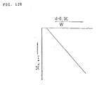
- Fig. 39 illustrates an example of the relation between the interstage magnetic field coupling coefficient and the center spacing of adjacent resonance capacity elements, obtained as a result of repeated experimentation with prototypes by the inventor.
- the axis of abscissa represents (d - 0.3C)/W where d is the center spacing of adjacent resonance capacity elements (see Fig. 33), C is the width of the resonance capacity element (see Fig. 33), and W is the width of the common external conductor (see Fig. 34).
- the axis of ordinate represents the interstage magnetic field coupling coefficient M k, k+1 .
- L (dB) 10 log ⁇ 1 + [(S - 1) 2 /4S]T 2 n (x) ⁇
- x is the normalized frequency
- f is an arbitrary transmission frequency
- Bwr is the permissible pass band frequency width
- S is the permissible voltage standing-wave ratio (VSWR) within the pass band.
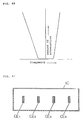
- Fig. 40 is a diagram illustrating an example of the transmission characteristics of the filter shown in Figs. 33 through 36.
- the axis of abscissa represents the frequency, and the axis of ordinate represents the amount of attenuation.
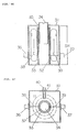
- Figs. 27, 30, 33, and 34 all give examples in which resonance capacity elements are provided such that the width directions of the resonance capacity elements CE1 through CE4 will be parallel to the lengthwise direction of the common external conductor IC , in all of the embodiments, as shown by the cross section of principal components in Fig. 41 (a cross section similar to Fig. 34), the present invention can also be implemented with the resonance capacity elements CE1 through CE4 arranged such that their width directions are at a right angle to the lengthwise direction of the common external conductor IC .
- a band-pass filter having the required transmission characteristics can be realized through suitable correction of the value of C in the axis of abscissa (d - 0.3C)/W of Fig. 39, which is used to determine the center spacing of the resonance capacity elements, or in other words, since the value of C corresponds to the width of the resonance capacity elements, through correction of the value of C to a value that corresponds to the thickness of the resonance capacity element when the resonance capacity elements are arranged as shown in Fig. 41.
- Fig. 42 is a vertical cross section of a band-pass filter in which the interstage coupling consists of capacitive coupling (a cross section at the same location as in Fig. 33).
- This filter comprises an external conductor 1C , resonance capacity elements CE1 through CE4 , an input terminal 5 , an output terminal 6 , an input coupling capacity element 2351 , interstage coupling capacity elements 2312 , 2323 , and 2334 , and an output coupling capacity element 2346 .
- Fig. 43 is an equivalent circuit diagram of the band-pass filter shown in Fig. 42.
- Symbols R1 through R4 represent resonance circuits
- the reference numeral 2351 represents the input coupling capacity
- reference numerals 2312 through 2334 represent interstage coupling capacities
- the reference numeral 2346 represents the output coupling capacity.
- Fig. 44 is a converted equivalent circuit diagram of the equivalent circuit diagram shown in Fig. 43.
- Fig. 42 shows an example in which the input/output coupling elements consist of capacity elements, tap coupling wires, probes, loops, or other such high-frequency coupling means may also be used.
- Fig. 45 is a diagram illustrating an example of the transmission characteristics of the band-pass filter shown in Fig. 42.
- the axis of abscissa represents the frequency, and the axis of ordinate represents the amount of attenuation.
- Fig. 46 is a vertical cross section of the resonator of the tenth embodiment according to the present invention.
- Fig. 47 is a horizontal cross section thereof.
- the resonator of this embodiment comprises a cubic external conductor 31 ; a variable resonance capacity element 32 made of a solid dielectric hollow cylinder, a fixed electrode 33 , and a movable electrode 34 ; a lock nut 35 that is used to fix the movable electrode 34 ; an input terminal 36 ; an output terminal 37 ; an input coupling wire 38 ; an output coupling wire 39 ; a resonance frequency fine-tuning element 40 ; and a lock nut 41 .
- the external conductor 31 may also be a bottomed cylinder.
- the lower end of the hollow cylinder 32 is fixed to the lower wall of the external conductor 31 by an adhesive agent or another suitable means, and the upper end faces the upper wall of the external conductor 31 a suitable distance away.
- the fixed electrode 33 is made of silver or another metal thin layer bonded around the outside of the hollow cylinder 32 , and the lower end thereof is electrically connected to the lower wall of the external conductor 31 by soldering or another suitable means.
- the movable electrode 34 is made of a solid or hollow cylindrical conductor (such as copper) with a threaded outside, and is screwed into the threaded hole in the upper wall of the external conductor 31 coaxially with the fixed electrode 33 .
- the insertion length of the movable electrode 34 into the hollow cylinder 32 , and therefore the insertion length of the movable electorde 34 into the fixed electrode 33 can be varied through the rotation of the movable electorde 34 in a forward or reverse direction to move the movable electrode 34 forward and backward.
- the movable electorde 34 can be fixed through the lock nut 35 .
- the input terminal 6 and the output terminal 7 consist, for example, of coaxial plugs, and the external conductor forming these coaxial plugs is connected to the external conductor 31 .
- the input coupling wire 38 is connected at one end to the internal conductor of the coaxial plug 36 , and at the other end to the fixed electrode 33 .
- the output coupling wire 39 is connected at one end to the internal conductor of the coaxial plug 37 , and at the other end to the fixed electrode 33 .
- the fine-tuning element 40 is made, for example, of a metal screw threaded into the wall of the external conductor 31 , and is fixed through the lock nut 41 .
- a parallel resonator circuit whose equivalent circuit is shown in Fig. 48, is formed by the distributed inductance of the external conductor 31 and the capacity of the variable resonance capacity element composed of the solid dielectric hollow cylinder 32 , the fixed electrode 33 , and the movable electrode 34 .
- the symbol R represents the resonance circuit
- the symbol M 6R represents the input magnetic field coupling coefficient
- the symbol M R7 represents the output magnetic field coupling coefficient.
- the electromagnetic field distribution in this resonator will be such that the electric field vector is expressed by the solid arrowed line E in Fig. 46, the current by the solid arrowed line I in Fig. 46, and the magnetic field by the broken line H in Fig. 47.
- this resonator is a low impedance type with good withstand voltage characteristics.
- the Q (Q u ) of the variable resonance capacity element composed of the solid dielectric hollow cylinder 32 , the fixed electrode 33 , and the movable electrode 34 can be ignored. Since the electromagnetic energy that can be accumulated in this resonator will correspond to the volume of the external conductor 31 , and the resistance in the metal portion of this resonator can be kept extremely low, an extremely large unloaded Q can be obtained.
- Fig. 46 illustrates an example in which tap coupling by the coupling wires 38 and 39 is used as means for coupling in high-frequency fashion the input terminal 36 with the fixed electrode 33 , and the output terminal 37 with the fixed electrode 33
- means for capacitively coupling the input terminal 36 with the fixed electrode 33 via the capacity element 42 and means for capacitively coupling the output terminal 37 with the fixed electrode 33 via the capacity element 43 may also be used, as shown in Fig. 49.
- probes 44 and 45 may be used as the input/output coupling means, as shown in Fig. 50, or loops 46 and 47 may be used as the input/output coupling means, as shown in Fig. 51.
- Figs. 49 through 51 correspond to cross sections of Fig. 47 viewed from below with the side wall on the bottom (from the front) removed from the external conductor 31 and hereinafter the same applies to cross sections similar to Figs. 49 through 51, such as Fig. 52.
- Fig. 52 is a vertical cross section of the resonator of the eleventh embodiment according to the present invention.
- a low-pass filter circuit is composed of inductance elements 48 and 49 for the compensation of transmission characteristics, interposed between the connection terminals 36 and 37 for the external circuit, and a capacity element 20 connected between the connection point of the inductance elements 48 and 49 and the fixed electrode 33 forming the resonance capacity element.
- the slope of the attenuation characteristic curve in the frequency region lower than the resonance frequency f0 is steep, while the slope of the attenuation characteristic curve in the frequency region higher than the resonance frequency f0 is gentle, and a transmission inhibition band is formed in the frequency region including the resonance frequency f0.
- Fig. 53 is an equivalent circuit diagram of the resonator shown in Fig. 52.
- the symbol R represents a resonance circuit composed of the external conductor 31 and the variable resonance capacity element, and the rest of the symbols are the same as in Fig. 52.
- the resonance frequency f0 of the circuit composed of the resonance circuit R and the coupling-use capacity element 52 changes according to the capacity of the coupling-use capacity element 50 , and the fine tuning of the resonance frequency can be performed by the provision of an adjustment element that is the same as the resonance frequency fine-tuning element 40 shown in Fig. 47.
- Fig. 55 is a vertical cross section of the resonator of the twelfth embodiment according to the present invention.
- This embodiment differs from the eleventh embodiment shown in Fig. 52 in that the coupling of the connection point of the inductance elements 48 and 49 with the fixed electrode 33 is performed by tap coupling using an inductance element 51 , and in that the resonance frequency f0 of the circuit composed of the resonance circuit R and the coupling-use inductance element 51 changes according to the inductance of the inductance element 51 .
- the rest of the structure and operation is substantially the same as in the eleventh embodiment shown in Fig. 52.
- Fig. 56 is an equivalent circuit diagram of the resonator shown in Fig. 55. Except for the inductance element 51 , all of the symbols are the same as in Fig. 53.
- Fig. 57 where the asix of abscissa and the axis of ordinate are the same as in Fig. 54, is a diagram illustrating the transmission characteristics of the resonator shown in Fig. 55, which is substantially the same as the characteristics shown in Fig. 54.
- Fig. 58 is a vertical cross section of the resonator of the thirteenth embodiment according to the present invention. This embodiment differs from the eleventh embodiment shown in Fig. 52 in that the inductance elements 48 and 49 used in the eleventh embodiment shown in Fig. 52 are replaced with capacity elements 52 and 53 . The rest of the structure is the same as in the eleventh embodiment shown in Fig. 52.
- Fig. 59 is an equivalent circuit diagram of the resonator shown in Fig. 58. Except for the capacity elements 52 and 53 , all of the symbols are the same as in Fig. 53.
- Fig. 60 where the axis of abscissa and the axis of ordinate are the same as in Fig. 54, is a diagram illustrating the transmission characteristics of the resonator shown in Fig. 58.
- the slope of the attenuation characteristic curve in the frequency region lower than the resonance frequency f0 is gentle, while the slope of the attenuation characteristic curve in the frequency region higher than the resonance frequency f0 is steep, and a transmission inhibition band is formed in the frequency region including the resonance frequency f0.
- Fig. 61 is a vertical cross section of the resonator of the fourteenth embodiment according to the present invention.
- This embodiment is the same as the embodiment shown in Fig. 58 in that the capacity elements 52 and 53 are used as transmission characteristic compensation elements, and is the same as the twelfth embodiment shown in Fig. 55 in that the coupling element is formed such that tap coupling will be performed using the inductance element 51 .
- the rest of the structure is the same as in the thirteenth embodiment shown in Fig. 58.
- Fig. 62 is an equivalent circuit diagram of the resonator shown in Fig. 61. Except for the inductance element 51 , all of the symbols are the same as in Fig. 59.
- Fig. 63 where the axis of abscissa and the axis of ordinate are the same as in Fig. 60, is a diagram illustrating the transmission characteristics of the resonator shown in Fig. 61, which is substantially the same as the characteristics shown in Fig. 60.
- Figs. 64 through 67 are cross sections illustrating the fifteenth through eighteenth embodiments according to the present invention.
- the resonator shown in Fig. 64 has a probe 44 in place of the coupling element 50 in the embodiment shown in Fig. 52;
- the resonator shown in Fig. 65 has a loop 46 in place of the coupling element 50 in the embodiment shown in Fig. 52;
- the resonator shown in Fig. 66 has a probe 44 in place of the coupling element 50 in the embodiment shown in Fig. 58 ;
- the resonator shown in Fig. 67 has a loop 46 in place of the coupling element 50 in the embodiment shown in Fig. 58.
- the rest of the structure in the respective Figs. is the same as the structure in Fig. 52 or 58.
- Fig. 68 is a vertical cross section of a filter constructed using the resonator shown in Fig. 46, and Fig. 69 is a horizontal cross section thereof.
- This filter comprises an external conductor 31C , fixed electrodes 331 through 334 which are the same as the fixed electrode 33 shown in Fig. 46, variable electrodes 341 through 344 that make up the variable resonance capacity element along with the fixed electrodes 331 through 334 and are the same as the movable electrode 34 shown in Fig. 46, lock nuts 351 through 354 which are used to fix the variable electrodes 341 through 344 , an input terminal 36 , an output terminal 37 , an input coupling wire 38 , an output coupling wire 39 , resonance frequency fine-tuning elements 401 through 404 , and lock nuts 411 through 414 that are used to fix the fine-tuning elements 401 through 404 .
- Fig. 70 is an equivalent circuit diagram of the filter shown in Figs. 68 and 69.
- Symbols R1 through R4 represent resonance circuits
- the symbol M61 represents the input magnetic field coupling coefficient
- the symbol M47 represents the output magnetic field coupling coefficient
- symbols M12 through M34 represent the interstage magnetic field coupling coefficients.
- Fig. 71 is a converted equivalent circuit diagram of the equivalent circuit diagram shown in Fig. 70, and the symbols are the same as in Fig. 70.
- Figs. 68 through 71 illustrate an example in which the input/output coupling elements is made of the tap coupling wires 38 and 39
- a capacity coupling element composed of the capacitors 42 and 43 or the probes 44 and 45 or a magnetic field coupling element composed of the loops 46 and 47 may also be used to implement the present invention, as shown in Figs. 49 through 51.
- the band-pass filter shown in Fig. 68 through 71 can be designed in the same manner as the band-pass filter shown in Figs. 33 through 36.
- Fig. 72 is a diagram illustrating an example of the relation between the interstage magnetic field coupling coefficient and the center spacing of adjacent resonance capacity elements, obtained as a result of repeated experimentation with prototypes by the inventor.
- the axis of abscissa represents (d - 0.3C)/W where d is the center spacing of adjacent resonance capacity elements (see Fig. 68), C is the external diameter of the fixed electrodes 331 through 334 that form the variable resonance capacity element (see Fig. 68), and W is the width of the external conductor 31C (see Fig. 69).
- the axis of ordinate represents the interstage magnetic field coupling coefficient M k, k+1 .
- FIG. 40 An example of the transmission characteristics of the filter shown in Figs. 68 through 71 is shown in Fig. 40.
- Fig. 73 is a vertical cross section of a band-pass filter in which the interstage coupling consists of capacitive coupling.
- This filter comprises an external conductor 31C , fixed electrodes 331 through 334 , lock nuts 351 through 354 , an input terminal 36 , an output terminal 37 , an input coupling capacity element 5461 , interstage coupling capacity elements 5412 through 5434 , and an output coupling capacity element 5447 .
- Fig. 74 is an equivalent circuit diagram of the band-pass filter shown in Fig. 73.
- Symbols R1 through R4 represent resonance circuits
- the reference numeral 5461 represents the input coupling capacity
- the reference numerals 5412 through 5434 represent the interstage coupling capacity
- the reference numeral 5447 represents the output coupling capacity.
- Fig. 75 is a converted equivalent circuit diagram of the equivalent circuit diagram shown in Fig. 74, and the symbols are the same as in Fig. 74.
- Fig. 73 shows an example in which the input/output coupling elements are made of capacity elements, tap coupling wires, probes, loops, or other such high-frequency coupling means may also be used.
- FIG. 40 An example of the transmission characteristics of the band-pass filter shown in Fig. 73 is shown in Fig. 40.
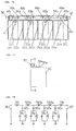
- Fig. 76 is a vertical cross section of a filter constructed using the resonator shown in Fig. 52.
- Fig. 77 is a right side view of Fig. 76.
- This filter comprises an external conductor 31C , partition walls 31S1 through 31S3 made of conductor plates, fixed electrodes 331 through 334 , movable electrodes 341 through 344 , lock nuts 351 through 354 that are used to fix the movable electrodes 341 through 344 , external circuit connection terminals 36 and 37 ; inductance elements 481 through 484 and 491 through 494 for the compensation of transmission characteristics, and coupling capacity elements 501 through 504 .
- Fig. 78 is an equivalent circuit diagram of the filter shown in Fig. 76.
- Symbols R1 through R4 represent resonance circuits comprising a common external conductor 31C and variable resonance capacity elements composed of fixed electrode 331 through 334 and movable electrodes 341 through 344 ;
- the reference numerals 481 , 4981 through 4983 , and 494 represent inductance elements for the compensation of transmission characteristics;
- the reference numeral 4981 represents a synthetic inductance element of the inductance elements 491 and 482 shown in Fig.
- the reference numeral 4982 represents a synthetic inductance element of the inductance elements 492 and 483
- the reference numeral 4983 represents a synthetic inductance element of the inductance elements 493 and 484
- the reference numerals 501 through 504 represent coupling-use capacity elements.
- the transmission characteristics of the filter shown in Fig. 76 is the superimposition of the transmission characteristics of the resonators at all stages composing this filter, that is, the superimposition of the transmission characteristics substantially the same as the transmission characteristics shown in Fig. 54.
- the resonance frequencies (f0 in Fig. 54) of all stages composed of a resonator and a coupling-use capacity element are represented by f01 through f04, respectively. Suitable adjustment of these resonance frequencies such that they approach each other, for instance, allows a region of inhibition with a large amount of attenuation to be realized, while adjustment of these resonance frequencies f01 through f04 to adequately separated values allows a region of inhibition with a wide range of frequency to be realized.
- Fig. 79 is an equivalent circuit diagram of a filter constructed using the filter shown in Fig. 55.
- Reference numerals 511 through 514 represent tap coupling-use inductance elements, and the rest of the symbols are the same as in Fig. 78.
- the transmission characteristics of this filter expressed by the equivalent circuit shown in Fig. 79 is the superimposition of the transmission characteristics of the resonators at all stages composing this filter, that is, the superimposition of the transmission characteristics substantially the same as the transmission characteristics shown in Fig. 57. Suitable adjustment of resonance frequency at each stage allows the frequency range and the amount of attenuation in the synthesis inhibition region to be suitably adjusted.
- Fig. 80 is a vertical cross section of a filter constructed using the resonator shown in Fig. 61.
- This filter comprises an external conductor 31C , partition walls 31S1 through 31S3 made of conductor plates, fixed electrodes 331 through 334 , movable electrodes 341 through 344 , external circuit connection terminals 36 and 37 , inductance elements 521 through 524 and 531 through 534 for the compensation of transmission characteristics and tap coupling inductance elements 511 through 514 .
- Fig. 81 is an equivalent circuit diagram of the filter shown in Fig. 80.
- Symbols R1 through R4 represent resonance circuits
- the reference numerals 5211 , 5321 through 5323 , and 534 represent capacity elements for the compensation of transmission characteristics
- the reference numeral 5321 represents a synthetic capacity element of the capacity elements 531 and 522 in Fig. 80
- the reference numeral 5322 represents a synthetic capacity element of the capacity elements 532 and 533
- the reference numeral 5323 represents a synthetic capacity element of the capacity elements 533 and 524
- the reference numerals 511 through 514 represent inductance elements for tap coupling.
- the transmission characteristics of the filter shown in Fig. 80 is the superimposition of the transmission characteristics of the resonators at all stages composing this filter, that is, the superimposition of the transmission characteristics substantially the same as the transmission characteristics shown in Fig. 63. Suitable adjustment of resonance frequency at each stage allows the frequency range and the amount of attenuation in the synthesis inhibition region to be suitably adjusted.
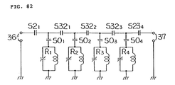
- Fig. 82 is an equivalent circuit diagram of a filter constructed using the resonator shown in Fig. 58.
- Reference numerals 201 through 204 represent coupling-use capacity elements, and the rest of the symbols are the same as in Fig. 81.
- the transmission characteristics of the filter expressed by the equivalent circuit shown in Fig. 82 is the superimposition of the transmission characteristics of the resonators at all the stages composing this filter, that is, the superimposition of the transmission characteristics substantially the same as the transmission characteristics shown in Fig. 60. Suitable adjustment of the resonance frequency at each stage allows the frequency range and the amount of attenuation in the synthesis inhibition region to be suitably adjusted.
- Figs. 68 through 82 illustrate examples in which four variable resonance capacity elements are provided, that is, when the order n of the circuit is 4, the present invention can also be implemented when the order n of the circuit is suitably increased or decreased.
- filters shown in Figs. 68 through 82 are Combline-type filters, the present invention can also be applied to interdigital filters.
- Fig. 83 is a vertical cross section of the resonator of the nineteenth embodiment according to the present invention, and Fig. 84 is a horizontal cross section thereof.
- the resonator of this embodiment comprises a cubic external conductor 61 ; a fixed electrode 62 made of a hollow cylindrical conductor, a movable electrode 63 ; a lock nut 64 that is used to fix the movable electrode 63 ; an input terminal 65 ; an output terminal 66 ; an input coupling loop 67 ; an output coupling loop 68 ; a resonance frequency fine-tuning element 69 ; and a lock nut 70 that is used to fix the fine-tuning element 69 .
- the external conductor 61 may also be a bottomed cylinder.
- the lower end of the fixed electrode 62 is fixed to the lower wall of the external conductor 61 , and the upper end faces the upper wall of the external conductor 61 a suitable distance away.
- the lower end of the fixed electrode 62 is fixed, for example, by screwing a flange that is integrally attached to the lower end of the fixed electrode 62 to the lower wall of the external conductor 61 .
- the movable electrode 63 is made of a solid or hollow cylindrical conductor (such as copper) with a threaded outside, and is screwed into the threaded hole formed in the upper wall of the external conductor 61 coaxially with the fixed electrode 62 .
- the insertion length of the movable electrode 63 into the holow cylinder 62 can be varied through the rotation of the movable electrode 62 in a forward or reverse direction to move the movable electrode 63 forward or backward.
- the input terminal 65 and the output terminal 66 is made, for example, of coaxial plugs, and the external conductor that forms these coaxial plugs is connected to the external conductor 61 .
- the fine-tuning element 69 is made, for example, of a metal screw threaded into the wall of the external conductor 61 .
- a parallel resonator circuit whose equivalent circuit is shown in Fig. 85, is formed by the distributed inductance in the external conductor 61 and the capacity in the variable resonance capacity element composed of the fixed electrode 62 and the movable electrode 63 .
- the symbol R represents the resonance circuit
- the symbol M 5R represents the input magnetic field coupling coefficient
- the symbol M R6 represents the output magnetic field coupling coefficient.
- the electromagnetic field distribution in this resonator will be such that the electric field vector is expressed by the solid arrowed line E in Fig. 83, the current by the solid arrowed line I , and the magnetic field by the broken line H in Fig. 84.
- this resonator is a low impedance type with good withstand voltage characteristics.
- the electromagnetic energy that can be accumulated in this resonator will correspond to the volume of the external conductor 61 , and the resistance in the metal portion of this resonator can be kept extremely low, so that an extremely large unloaded Q can be obtained.
- the inventor was able to obtain the following experimental equation (15) for the unloaded Q (Q u ) through the use of prototypes whose external conductor 61 , the fixed electrode 62 , and the movable electrode 63 of this resonator are made of copper, although the magnitude of the unloaded Q (Q u ) will vary with the ratio of inductance to the capacity of the resonator.
- Q u ⁇ 20 f 0 1 ⁇ 2 ⁇ SH where f0 is the resonance frequency (MHz) and SH is the height (cm) of the external conductor 61 (see Fig. 83).
- Fig. 83 illustrates an example in which a resonance frequency fine-tuning element 69 and a lock nut 70 are provided, the present invention can also be implemented with these components omitted. Also, Fig. 83 illustrates an example in which loops 67 and 68 are provided as means for coupling in high-frequency fashion the input terminal 65 with the fixed electrode 62 and the output terminal 66 with the fixed electrode 62 , means for capacitively coupling the input terminal 65 with the fixed electrode 62 via the capacity element 71 and means for capacitively coupling the output terminal 66 with the fixed electrode 62 via the capacity element 72 may also be used, as shown in Fig. 86.
- probes 73 and 74 may be used as the input/output coupling means, as shown in Fig. 87, or tap coupling may be performed using coupling wires 75 and 76 as the input/output coupling means, as shown in Fig. 88.
- Figs. 86 through 88 are the cross sections of Fig. 84, omitting the lower side wall of the external conductor 61 .
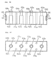
- Fig. 89 is a vertical cross section of a filter constructed using the resonator shown in Fig. 83, and Fig. 90 is a horizontal cross section thereof.
- This filter comprises an external conductor 61C , fixed electrodes 621 through 624 , movable electrodes 631 through 634 , lock nuts 641 through 644 that are used to fix the movable electrodes 631 through 634 , an input terminal 65 , an output terminal 66 , an input coupling loop 67 , and an output coupling loop 68 .
- Fig. 91 is an equivalent circuit diagram of the filter shown in Figs. 89 and 90.
- Symbols R1 through R4 represent resonance circuits
- the symbol M51 represents the input magnetic field coupling coefficient
- the symbol M46 represents the output magnetic field coupling coefficient
- symbols M12 through M34 represent the interstage magnetic field coupling coefficients.
- Fig. 92 is a converted equivalent circuit diagram of the equivalent circuit diagram shown in Fig. 91, and the symbols are the same as in Fig. 91.
- the band-pass filter shown in Figs. 89 through 92 can be designed in the same manner as the band-pass filter shown in Figs. 33 through 36.
- Fig. 93 illustrates an example of the relation between the interstage magnetic field coupling coefficient and the center spacing of adjacent resonance capacity elements, obtained as a result of repeated experimentation with prototypes by the inventor.
- the axis of abscissa represents (d - 0.3C)/W where d is the center spacing of adjacent resonance capacity elements (see Fig. 90), C is the external diameter of each of the fixed electrodes 21 through 24 that form the variable resonance capacity element (see Fig. 89), and W is the width of the common shield case 61C (see Fig. 90).
- the axis of ordinate represents the interstage magnetic field coupling coefficient M k, k+1 .
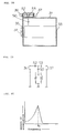
- Fig. 94 is a diagram illustrating an example of the transmission characteristics over the wide band of the filter shown in Figs. 89 through 92.
- the axis of abscissa represents the frequency (MHz), with graduations of 300 MHz and a resonance frequency f0 of 565 MHz, while the axis of ordinate represents the amount of attenuation (dB), with graduations of 10 dB.
- Fig. 95 is an enlarged transmission characteristics diagram near the resonance frequency f0 in Fig. 94.
- the axis of abscissa represents the frequency (MHz), with graduations of 5 MHz, while the axis of ordinate represents the amount of attenuation (dB), with graduations of 5 dB.
- the harmonic components of the resonance frequency f0 are greatly attenuated, since this characteristic is also a characteristic of the resonators composing this filter, the resonator shown in Fig. 83 will have substantially the same characteristics as a lumped constant type of resonator composed of a coil and a capacitor, which are lumped-constant circuit elements.
- the irregular waveform present near an attenuation of -80 dB to -100 dB in Fig. 94 is believed to be noise admixed in the measurement device circuit.
- the filter shown in Figs. 89 through 92 is constructed such that the required electrical characteristics will be obtained by setting the center spacing of the variable resonance capacity elements according to the required interstage magnetic field coupling coefficient, the required electrical characteristics can also be obtained by arranging the variable resonance capacity elements at a suitable fixed interval and interposing conventional interstage magnetic field coupling adjustment elements between adjacent variable resonance capacity elements.
- Fig. 96 is a vertical cross section illustrating an example of the above, and Fig. 97 is a horizontal cross section of the same.
- reference numerals 7711 through 7732 represent conventional interstage magnetic field coupling adjustment elements made of round or square rod-shaped or ribbon-shaped conductors.
- the axial direction of the interstage magnetic field coupling adjustment elements 7711 through 7732 between adjacent fixed electrodes 621 and 622 , 622 and 623 , and 623 and 624 is parallel to the axial direction of the fixed electrodes 621 through 624 , and the both ends of each of the interstage magnetic field coupling adjustment elements 7711 through 7732 are electrically and mechanically connected to the upper and lower walls of the common shield case 61C .
- the interstage magnetic field coupling coefficient can be adjusted to the required value by forming each of the interstage magnetic field coupling adjustment elements 7711 through 7732 in a suitable thickness, or by suitably increasing or decreasing the number of interstage magnetic field coupling adjustment elements interposed between the adjacent variable resonance capacity elements.
- Fig. 98 is also a vertical cross section of a filter constructed such that the interstage magnetic field coupling coefficient is adjusted by means of interstage magnetic field coupling adjustment elements
- Fig. 99 is a horizontal cross section thereof.
- reference numerals 781 through 783 represent conventional interstage magnetic field coupling adjustment elements in the shape of a plate.
- Each plate is at a right angle to the lengthwise direction of the common shield case 61C between adjacent fixed electrodes 621 and 622 , 622 and 623 , and 623 and 624 , each edge of the plate is electrically connected to the upper and lower walls and both side walls of the common shield case 61C , and a magnetic field coupling hole is formed in each plate.
- the interstage magnetic field coupling coefficient can be suitably adjusted according to the surface area of the magnetic field coupling holes formed in the interstage magnetic field coupling adjustment elements 781 through 783 .
- Fig. 100 is a vertical cross section of another example of a filter constructed using the resonator shown in Fig. 83.
- This filter comprises an external conductor 61C , fixed electrodes 621 through 624 , movable electrodes 631 through 634 , lock nuts 641 through 644 that are used to fix the movable electrodes 631 through 634 , an input terminal 65 , and output terminal 66 , an input coupling-use probe 73 , an output coupling-use probe 74 , partition walls 791 through 793 made of conductor plates, capacity formation electrodes 8011 through 8032 , and connection conductors 811 through 813 .
- connection conductors 811 through 813 are inserted through and fixed to the partition walls 791 through 793 while maintaining insulation between connection conductors 81 1 through 813 and the partition walls 791 through 793 .
- the connection conductor 811 connects the electrodes 8011 with the electrode 8012 , and capacitively couples the resonator including the fixed electrode 621 with the resonator including the fixed electrode 622 .
- the other resonators are similarly coupled.
- Fig. 101 is also a vertical cross section of a filter in which the neighbouring stages are coupled by capacitive coupling.
- capacity formation electrodes 821 through 823 having U-shaped cross sections, and rotary support shafts 831 through 833 that are rotatably attached to the upper wall of the common shield case 61C maintaining insulation between the support shafts 83 1 through 833 and the upper wall of the common shield case 61C , are provided in place of the partition walls 791 through 793 , the capacity formation electrodes 8011 through 8032 , and the connection conductors 811 through 813 of the filter in Fig. 100.
- the support shaft 831 When the support shaft 831 is rotated, the electrode 821 supported by this support shaft 831 also rotates, thereby changing the interstage coupling capacity coefficient.
- the other neighbouring stages are similarly coupled.
- the filters in the embodiments shown in Figs. 89, 90, and 96 through 101 are examples of cases in which the order of the circuit is 4, the present invention can also be implemented with this order suitably increased or decreased.
- the resonators shown in Figs. 83 and 86 through 88 can be operated as a band elimination filter by connecting one of the terminals to an external circuit using one of the methods shown in Figs. 52, 55, 58, 61, 64 through 67, and so on.
- a band elimination filter of which the elimination band width, the amount of attenuation, etc., can be set and changed at will can be constructed by replacing the various variable capacity elements in Figs. 76 through 82 with the variable capacity element in Fig. 83.
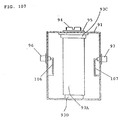
- Fig. 102 is a vertical cross section of the resonator of the twentieth embodiment according to the present invention
- Fig. 103 is a horizontal cross section thereof.
- the resonator in this embodiment comprises a cubic external conductor 91 ; a solid dielectric hollow cylinder 92 made of ceramic; a variable resonance capacity element composed of fixed electrodes 93A and 93B , and a movable electrode 94 ; a fixing member 93C that is used to fix the fixed electrode 93A , a fixing member 93D that is used to fix the fixed electrode 93B , a lock nut 95 that is used to fix the movable electrode 94 ; an input terminal 96 ; an output terminal 97 ; an input coupling wire 98 ; an output coupling wire 99 ; a resonance frequency fine-tuning element 100 ; and a lock nut 101 .
- the external conductor 91 may also be a bottomed cylinder.
- the upper and lower ends of the hollow cylinder 92 are a suitable distance apart from, and face the upper and lower walls, respectively, of the external conductor 91 .
- the fixed electrode 93A , 93B are made of a metal thin layer such as silver that is bonded-around the inside and outside, respectively, of the hollow cylinder 92 .
- the upper end of the fixed electrode 93A is soldered to the inner side of the conductive fixing member 93C , which is in the form of a flanged hollow cylinder, and the flange of the fixing member 93C is fixed by a screw to the upper wall of the external conductor 91 .
- the lower end of the fixed electrode 93B is attached in elastic contact with the upper portion of the conductive fixing member 93D whose upper portion is provided with a plurality of slits to achieve elasticity and which is in the form of a bottomed hollow cylinder.
- This fixing member 93D is fixed to the lower wall of the external conductor 91 by a screw, using the threaded hole formed in the bottom of itself.
- the movable electrode 94 made of a solid or hollow cylindrical conductor (such as copper) threaded around its outside, and is screwed into the threaded hole formed in the upper wall of the external conductor 91 coaxially with the fixed electrodes 93A and 93B .
- the insertion length of the movable electrode 94 into the hollow cylinder 92 , and therefore the insertion length of the movable electrode 94 into the fixed electrode 93B can be varied by the rotation of the movable electrode 94 in a forward or reverse direction to move the movable electrode 94 forward or backward.
- the movable electrode 94 is fixed by the lock nut 95 .
- the input terminal 96 and the output terminal 97 consist, for example, of coaxial plugs, and the external conductor that forms these coaxial plugs is connected to the external conductor 91 .
- the input coupling wire 98 is connected at one end to the internal conductor of the coaxial plug 96 , and at the other end to the fixed electrode 93A .
- the output coupling wire 99 is connected at one end to the internal conductor of the coaxial plug 97 , and at the other end to the fixed electrode 93A .
- the fine-tuning element 100 is made of a metal screw threaded into the wall of the external conductor 91 , and is fixed by a lock nut 101 .
- a parallel resonance circuit whose equivalent circuit is shown in Fig. 104, is formed by the distributed inductance of the external conductor 91 and the capacity of the variable resonance capacity element composed of the solid dielectric hollow cylinder 92 , the fixed electrodes 93A and 93B , and the movable electrode 94 .
- the symbol R represents the resonance circuit
- the symbol M 6R represents the input magnetic field coupling coefficient
- the symbol M R7 represents the output magnetic field coupling coefficient.
- the electromagnetic field distribution in this resonator will be such that the electric field vector is expressed by the solid arrowed line E in Fig. 102, the current by the solid arrowed line I in Fig. 102, and the magnetic field by the broken line H in Fig. 103.
- this resonator is a low impedance type with good withstand voltage characteristics.
- the Q (Q u ) of the variable resonance capacity element consisting of the solid dielectric hollow cylinder 92 , the fixed electrodes 93A and 93B , and the movable electrode 94 can be ignored.
- the electronic energy that can be accumulated in this resonator will correspond to the volume of the external conductor 91 , and the resistance in the metal portion of this resonator can be kept extremely low, so that an extremely large unloaded Q can be obtained.
- Fig. 102 illustrates an example of a case in which tap coupling by the coupling wires 98 and 99 is used as means for coupling in high-frequency fashion the input terminal 96 with the fixed electrode 93A , and the output terminal 97 with the fixed electrode 93A
- means for capacitively coupling the input terminal 96 with the fixed electrode 93A via the capacity element 102 and means for capacitively coupling the output terminal 97 with the fixed electrode 93A via the capacity element 103 may also be used, as shown in Fig. 105, or probes 104 and 105 may be used as the input/output coupling means, as shown in Fig. 106.
- loops 106 and 107 may be used as the input/output coupling means, as shown in Fig. 107.
- Figs. 105 through 107 correspond to the cross section of Fig. 103 viewed from below, omitting the lower side wall of external conductor 91 , and hereinafter the same applies to Fig. 108 similar to Figs. 105 through 107.
- Fig. 108 is a vertical cross section of the resonator of the twenty-first embodiment according to the present invention.
- a low-pass filter circuit is formed by inductance elements 108 and 109 for the compensation of transmission characteristics, interposed between the connection terminals 96 and 97 with the external circuit, and a capacity element 110 connected between the fixed electrode 93A that forms the resonance capacity element and the connection point of the inductance elements 108 and 109 .
- the slope of the attenuation characteristic curve in the frequency region lower than the resonance frequency f0 is steep, while the slope of the attenuation characteristic curve in the frequency region higher than the resonance frequency f0 is gentle, and a transmission inhibition band is formed in the frequency region including the resonance frequency f0.
- Fig. 109 is an equivalent circuit diagram of the resonator shown in Fig. 108.
- the symbol R represents the resonance circuit composed of the external conductor 91 and the variable resonance capacity element, and the rest of the symbols are the same as in Fig. 108.
- the resonance frequency f0 of the circuit composed of the resonance circuit R and the coupling-use capacity element 112 changes according to the capacitance of the coupling-use capacity element 110 , and the fine tuning of the resonance frequency can be performed by the provision of an adjustment element similar to the resonance frequency fine-tuning element 100 shown in Fig. 103.
- Fig. 111 is a vertical cross section of the resonator of the twenty-second embodiment according to the present invention.
- This embodiment differs from the twenty-first embodiment shown in Fig. 108 in that the coupling of the connection point of the inductance elements 108 and 109 with the fixed electrode 93A is performed by tap coupling using an inductance element 111 , and in that the resonance frequency f0 of the circuit composed of the resonance circuit R and the coupling-use inductance element 111 changes according to the inductance of the inductance element 111 .
- the rest of the structure and operation is substantially the same as in the twenty-first embodiment shown in Fig. 108.
- Fig. 112 is an equivalent circuit diagram of the resonator shown in Fig. 111. Except for the inductance element 111 , all of the symbols are the same as in Fig. 109.
- Fig. 113 where the axis of abscissa and the axis of ordinate are the same as in Fig. 110, is a diagram illustrating the transmission characteristics of the resonator shown in Fig. 111, which is substantially the same as the characteristics shown in Fig. 110.
- Fig. 114 is a vertical cross section of the resonator of the twenty-third embodiment according to the present invention. This embodiment differs from the twenty-first embodiment shown in Fig. 108 in that the inductance elements 108 and 109 used in the twenty-first embodiment shown in Fig. 108 are replaced with capacity elements 112 and 113 . The rest of the structure is the same as in the twenty-first embodiment shown in Fig. 108.
- Fig. 115 is an equivalent circuit diagram of the resonator shown in Fig. 114. Except for the capacity elements 112 and 113 , all of the symbols are the same as in Fig. 109.
- Fig. 116 where the axis of abscissa and the axis of ordinate are the same as in Fig. 110, is a diagram illustrating the transmission characteristics of the resonator shown in Fig. 114.
- the slope of the attenuation characteristic curve in the frequency region lower than the resonance frequency f0 is gentle, while the slope of the attenuation characteristic curve in the frequency region higher than the resonance frequency f0 is steep, and a transmission inhibition band is formed in the frequency region including the resonance frequency f0.
- Fig. 117 is a vertical cross section of the resonator of the twenty-fourth embodiment according to the present invention.
- This embodiment is the same as the twenty-third embodiment shown in Fig. 115 in that the capacity elements 112 and 113 are used as transmission characteristic compensation elements, and is the same as the twenty-second embodiment shown in Fig. 111 in that tap coupling is performed using the inductance element 111 as a coupling element.
- the rest of the structure is the same as in the twenty-third embodiment shown in Fig. 114.
- Fig. 118 is an equivalent circuit diagram of the resonator shown in Fig. 117. Except for the inductance element 111 , all of the symbols are the same as in Fig. 115.
- Fig. 119 where the axis of abscissa and the axis of ordinate are the same as in Fig. 116, is a diagram illustrating the transmission characteristics of the resonator shown in Fig. 117, which is substantially the same as the characteristics shown in Fig. 116.
- Figs. 120 through 123 are cross sections illustrating the twenty-fifth through twenty-eighth embodiments of the present invention.
- the resonator in Fig. 120 has a probe 104 in place of the coupling element 110 shown in Fig. 108; the resonator in Fig. 121 has a loop 106 in place of the coupling element 110 shown in Fig. 108; the resonator in Fig. 122 has a probe 104 in place of the coupling element 110 shown in Fig. 114; and the resonator in Fig. 123 has a loop 106 in place of the coupling element 110 shown in Fig. 114.
- the rest of the structure in the respective figs. are the same as the structure in Fig. 108 or 114.
- Fig. 124 is a vertical cross section of a filter constructed using the resonator shown in Fig. 102, and Fig. 125 is a horizontal cross section thereof.
- This filter comprises an external conductor 91C ; fixed electrodes 93A1 through 93A4 and 93B1 through 93B4 similar to the fixed electrodes 93A and 93B shown in Fig. 102; solid dielectric hollow cylinders 921 through 924 similar to the solid dielectric hollow cylinder 92 shown in Fig.
- variable electrodes 941 through 944 that make up the variable resonance capacity element along with the fixed electrodes 93A1 through 93A4 and 93B1 through 93B4 and are similar to the movable electrode 94 shown in Fig.
- lock nuts 951 through 954 that are used to fix the variable electrodes 941 through 944 ; an input terminal 96 ; an output terminal 97 ; an input coupling wire 98 ; an output coupling wire 99; resonance frequency fine-tuning elements 1001 through 1004 ; and lock nuts 1011 through 1014 that are used to fix the fine-tuning elements 1001 through 1004 .
- Fig. 126 is an equivalent circuit diagram of the filter shown in Figs. 124 and 125.
- Symbols R1 through R4 represent resonance circuits
- the symbol M61 represents the input magnetic field coupling coefficient
- the symbol M47 represents the output magnetic field coupling coefficient
- symbols M12 through M34 represent the interstage magnetic field coupling coefficients.
- Fig. 127 is a converted equivalent circuit diagram of the equivalent circuit diagram shown in Fig. 126, and the symbols are the same as in Fig. 126.
- Figs. 124 through 127 illustrate a case in which the input/output coupling elements are made of the tap coupling wires 98 and 99
- a capacity coupling element made of the capacitors 102 and 103 or the probes 104 and 105 or a magnetic field coupling element made of the loops 106 and 107 shown in Figs. 105 through 107 may also be used to implement the present invention.
- the band-pass filter shown in Figs. 124 through 127 can be designed in the same manner as the band-pass filter shown in Figs. 33 through 36.
- Fig. 128 illustrates an example of the relation between the interstage magnetic field coupling coefficient and the center spacing of adjacent resonance capacity elements, obtained as a result of repeated experimentation with prototypes by the inventors.
- the axis of abscissa represents (d - 0.3C)/W where d is the center spacing of adjacent resonance capacity elements (see Fig. 124), C is the external diameter of the fixed electrodes 93A1 through 93A4 that form the variable resonance capacity element (see Fig. 124), and W is the width of the external conductor 91C (see Fig. 125).
- the axis of ordinate represent the interstage magnetic field coupling coefficient M k, k+1 .
- FIG. 40 An example of the transmission characteristics of the filter shown in Figs. 124 through 127 is shown in Fig. 40.
- Fig. 129 is a vertical cross section of a band-pass filter in which the interstage coupling consists of capacitive coupling.
- This filter comprises an external conductor 91C ; fixed electrodes 93A1 through 93A4 , solid dielectric hollow cylinders 921 through 924 and fixed electrodes 93B1 through 93B4 that are provided concentrically to the interiors of the fixed electrodes 93A1 through 93A4 , although not shown in the Fig. 129; fixing members 93C1 through 93C4 ; fixing members 93D1 through 93D4 ; lock nuts 951 through 954 ; an input terminal 96 ; an output terminal 97 ; an input coupling capacity element 11461 ; interstage coupling capacity elements 11412 through 11434 ; and an output coupling capacity element 11447 .
- Fig. 130 is an equivalent circuit diagram of the band-pass filter shown in Fig. 129.
- Symbols R1 through R4 represent resonance circuits
- the reference numeral 11461 is the input coupling capacity
- reference numeral 11412 through 11434 represent the interstage coupling capacity
- the reference numerals 11447 represent the output coupling capacity.
- Fig. 131 is a converted equivalent circuit diagram of the equivalent circuit diagram shown in Fig. 130, and the symbols are the same as in Fig. 130.
- Fig. 129 illustrates an example of a case in which the input/output coupling elements consist of capacity elements, tap coupling wires, probes, loops, or other such high-frequency coupling means may also be used.
- FIG. 40 An example of the transmission characteristics of the band-pass filter shown in Fig. 129 is shown in Fig. 40.
- variable resonance capacity element shown in Fig. 102 (comprising the solid dielectric hollow cylinder 92 , the fixed electrodes 93A and 93B , the fixing members 93C and 93D , the movable electrode 94 , and the lock nut 95 ) instead of the variable resonance capacity element of the filter in Fig. 76 or 80 (comprising the solid dielectric hollow cylinder 32 , the fixed electrode 33 , the movable electrode 34 , and the lock nut 35 of the resonator shown in Fig. 46 ).
- the transmission characteristics will be the same as the transmission characteristics of the filter in Fig. 76 or 80 except that the usable frequency band will be lower because of the fixed capacity produced by the solid dielectric hollow cylinder 92 and the fixed electrodes 93A and 93B .
- the fixed electrodes 93A and 93B can be constructed from a hollow cylinder made of a metal conductor that has been strengthened by making the walls thicker, and an air layer can be used instead of the hollow cylinder 92 made of a solid dielectric.
Landscapes
- Physics & Mathematics (AREA)
- Electromagnetism (AREA)
- Control Of Motors That Do Not Use Commutators (AREA)
Applications Claiming Priority (10)
| Application Number | Priority Date | Filing Date | Title |
|---|---|---|---|
| JP6087807A JP2631268B2 (ja) | 1994-03-31 | 1994-03-31 | 共振器及びこの共振器より成るろ波器 |
| JP87807/94 | 1994-03-31 | ||
| JP8780794 | 1994-03-31 | ||
| JP28412494 | 1994-10-25 | ||
| JP284124/94 | 1994-10-25 | ||
| JP28412494A JPH08125405A (ja) | 1994-10-25 | 1994-10-25 | 共振器及びこの共振器より成るろ波器 |
| JP5197195 | 1995-02-15 | ||
| JP51971/95 | 1995-02-15 | ||
| JP5197195A JPH08222915A (ja) | 1995-02-15 | 1995-02-15 | 共振器及びこの共振器より成るろ波器 |
| PCT/JP1995/000629 WO1995027318A1 (fr) | 1994-03-31 | 1995-03-31 | Cavite resonante et filtre utilisant cet element |
Publications (3)
| Publication Number | Publication Date |
|---|---|
| EP0703634A1 true EP0703634A1 (fr) | 1996-03-27 |
| EP0703634A4 EP0703634A4 (fr) | 1996-07-24 |
| EP0703634B1 EP0703634B1 (fr) | 2003-02-26 |
Family
ID=27294500
Family Applications (1)
| Application Number | Title | Priority Date | Filing Date |
|---|---|---|---|
| EP95913401A Expired - Lifetime EP0703634B1 (fr) | 1994-03-31 | 1995-03-31 | Cavite resonante et filtre utilisant cet element |
Country Status (7)
| Country | Link |
|---|---|
| US (1) | US5691675A (fr) |
| EP (1) | EP0703634B1 (fr) |
| KR (1) | KR100323895B1 (fr) |
| CN (1) | CN1111923C (fr) |
| DE (1) | DE69529715T2 (fr) |
| FI (1) | FI115425B (fr) |
| WO (1) | WO1995027318A1 (fr) |
Cited By (3)
| Publication number | Priority date | Publication date | Assignee | Title |
|---|---|---|---|---|
| GB2312993A (en) * | 1996-05-07 | 1997-11-12 | Adc Solitra Oy | Radio-frequency resonant filter arrangement |
| WO1998028813A3 (fr) * | 1996-12-20 | 1998-09-11 | Ericsson Telefon Ab L M | Boucle reglable fixe |
| US9515362B2 (en) | 2010-08-25 | 2016-12-06 | Commscope Technologies Llc | Tunable bandpass filter |
Families Citing this family (9)
| Publication number | Priority date | Publication date | Assignee | Title |
|---|---|---|---|---|
| SE513293C2 (sv) * | 1998-12-18 | 2000-08-21 | Ericsson Telefon Ab L M | Fästanordning vid kontaktövergång |
| US6404307B1 (en) | 1999-12-06 | 2002-06-11 | Kathrein, Inc., Scala Division | Resonant cavity coupling mechanism |
| US6329305B1 (en) | 2000-02-11 | 2001-12-11 | Agere Systems Guardian Corp. | Method for producing devices having piezoelectric films |
| SE527798C2 (sv) * | 2004-10-19 | 2006-06-07 | Powerwave Technologies Sweden | Ett DC-extraherande arrangemang |
| EP2882033A1 (fr) * | 2013-12-09 | 2015-06-10 | Centre National De La Recherche Scientifique | Résonateur et filtre radiofréquence |
| US9755288B2 (en) * | 2014-09-29 | 2017-09-05 | Alcatel-Lucent Shanghai Bell Co., Ltd. | Methods and devices for integrating radio frequency and other signals within a conductor |
| WO2016164603A1 (fr) * | 2015-04-07 | 2016-10-13 | Plasma Igniter, LLC | Coupleur et filtre directionnels à radiofréquence |
| WO2016174424A2 (fr) * | 2015-04-28 | 2016-11-03 | David Rhodes | Filtre à micro-ondes accordable et multiplexeur de micro-ondes accordable |
| CN111404510A (zh) | 2020-04-21 | 2020-07-10 | 安徽安努奇科技有限公司 | 谐振电路和滤波器件 |
Family Cites Families (16)
| Publication number | Priority date | Publication date | Assignee | Title |
|---|---|---|---|---|
| CH315733A (de) * | 1953-08-26 | 1956-08-31 | Patelhold Patentverwertung | Schwingsystem für Ultrakurzwellen |
| US4053856A (en) * | 1976-02-03 | 1977-10-11 | Fisher Sidney T | Quasi-toroidal inductor and resonator |
| JPS5535560A (en) * | 1978-09-04 | 1980-03-12 | Matsushita Electric Ind Co Ltd | Coaxial type filter |
| DE2947519C2 (de) * | 1979-11-24 | 1983-02-10 | Herfurth Gmbh, 2000 Hamburg | Schwingkreisanordnung |
| JPS6218963Y2 (fr) * | 1980-01-11 | 1987-05-15 | ||
| JPS5879301A (ja) * | 1981-11-06 | 1983-05-13 | Mitsubishi Electric Corp | 高周波ろ波器 |
| JPS58105602A (ja) * | 1981-12-18 | 1983-06-23 | Fujitsu Ltd | 誘電体フイルタ |
| JPS5915304A (ja) * | 1982-07-15 | 1984-01-26 | Matsushita Electric Ind Co Ltd | 同軸型誘電体共振器 |
| FR2535547B1 (fr) * | 1982-10-29 | 1988-09-16 | Thomson Csf | Resonateurs bi-rubans et filtres realises a partir de ces resonateurs |
| US4614925A (en) * | 1983-07-05 | 1986-09-30 | Matsushita Electric Industrial Co., Ltd. | Resonator filters on dielectric substrates |
| JPS6014504A (ja) * | 1983-07-05 | 1985-01-25 | Matsushita Electric Ind Co Ltd | 同調器 |
| US4568985A (en) * | 1983-07-11 | 1986-02-04 | Datacopy Corporation | Electronic camera scanning mechanism |
| GB2163009B (en) * | 1984-08-10 | 1987-11-04 | Marconi Co Ltd | High-frequency electrical network |
| JPS6161503A (ja) * | 1984-08-31 | 1986-03-29 | Murata Mfg Co Ltd | 誘電体共振器 |
| JPH01103001A (ja) * | 1987-10-15 | 1989-04-20 | Murata Mfg Co Ltd | 誘電体フィルタ |
| SU1741200A1 (ru) * | 1989-05-11 | 1992-06-15 | Новосибирский электротехнический институт связи им.Н.Д.Псурцева | Перестраиваемый резонатор |
-
1995
- 1995-03-31 US US08/556,905 patent/US5691675A/en not_active Expired - Fee Related
- 1995-03-31 EP EP95913401A patent/EP0703634B1/fr not_active Expired - Lifetime
- 1995-03-31 KR KR1019950705375A patent/KR100323895B1/ko not_active Expired - Fee Related
- 1995-03-31 CN CN95190422A patent/CN1111923C/zh not_active Expired - Fee Related
- 1995-03-31 DE DE69529715T patent/DE69529715T2/de not_active Expired - Fee Related
- 1995-03-31 WO PCT/JP1995/000629 patent/WO1995027318A1/fr not_active Ceased
- 1995-11-29 FI FI955759A patent/FI115425B/fi not_active IP Right Cessation
Cited By (6)
| Publication number | Priority date | Publication date | Assignee | Title |
|---|---|---|---|---|
| GB2312993A (en) * | 1996-05-07 | 1997-11-12 | Adc Solitra Oy | Radio-frequency resonant filter arrangement |
| GB2312993B (en) * | 1996-05-07 | 1998-07-01 | Adc Solitra Oy | Filter |
| US5874872A (en) * | 1996-05-07 | 1999-02-23 | Adc Solitra Oy | Filter |
| WO1998028813A3 (fr) * | 1996-12-20 | 1998-09-11 | Ericsson Telefon Ab L M | Boucle reglable fixe |
| US6005452A (en) * | 1996-12-20 | 1999-12-21 | Telefonaktiebolget Lm Ericsson | Fixed tuneable loop |
| US9515362B2 (en) | 2010-08-25 | 2016-12-06 | Commscope Technologies Llc | Tunable bandpass filter |
Also Published As
| Publication number | Publication date |
|---|---|
| KR960703278A (ko) | 1996-06-19 |
| FI955759A0 (fi) | 1995-11-29 |
| KR100323895B1 (ko) | 2002-06-24 |
| EP0703634A4 (fr) | 1996-07-24 |
| CN1111923C (zh) | 2003-06-18 |
| WO1995027318A1 (fr) | 1995-10-12 |
| CN1128585A (zh) | 1996-08-07 |
| EP0703634B1 (fr) | 2003-02-26 |
| FI955759L (fi) | 1996-01-22 |
| US5691675A (en) | 1997-11-25 |
| DE69529715T2 (de) | 2003-09-11 |
| FI115425B (fi) | 2005-04-29 |
| DE69529715D1 (de) | 2003-04-03 |
Similar Documents
| Publication | Publication Date | Title |
|---|---|---|
| US5319328A (en) | Dielectric filter | |
| FI78198C (fi) | Oeverfoeringsledningsresonator. | |
| US4578656A (en) | Microwave microstrip filter with U-shaped linear resonators having centrally located capacitors coupled to ground | |
| US4386328A (en) | High frequency filter | |
| US5691675A (en) | Resonator with external conductor as resonance inductance element and multiple resonator filter | |
| US4757285A (en) | Filter for short electromagnetic waves formed as a comb line or interdigital line filters | |
| CA2094314A1 (fr) | Resonateur helicoidal | |
| CA2352166A1 (fr) | Filtres accordables electriquement a varactors dielectriques | |
| US2527608A (en) | Constant impedance network | |
| US4682131A (en) | High-Q RF filter with printed circuit board mounting temperature compensated and impedance matched helical resonators | |
| US3959749A (en) | Filter of the distributed constants type | |
| KR0141975B1 (ko) | 절연된 필터 단을 갖는 다단 모노리딕식 세라믹 대역 소거 필터 | |
| US3936776A (en) | Interspersed double winding helical resonator with connections to cavity | |
| US2892163A (en) | Band-pass filters | |
| JP2655133B2 (ja) | 共振器及びこの共振器より成るろ波器 | |
| US4075583A (en) | Low loss tuneable filter | |
| JPH08222915A (ja) | 共振器及びこの共振器より成るろ波器 | |
| JPH0416012A (ja) | ノイズ・フイルタ | |
| JP2631268B2 (ja) | 共振器及びこの共振器より成るろ波器 | |
| JPH0229241B2 (ja) | Taiikitsukarohaki | |
| JP2516857B2 (ja) | リング共振器及びこのリング共振器を用いたろ波器 | |
| JPH11214905A (ja) | 共振器及びこの共振器を用いたフィルタ | |
| JPH08125405A (ja) | 共振器及びこの共振器より成るろ波器 | |
| JPH06188607A (ja) | ノッチフィルタ及びこのノッチフィルタを用いて成るノッチダイプレクサ | |
| JPH05183305A (ja) | 帯域通過ろ波器 |
Legal Events
| Date | Code | Title | Description |
|---|---|---|---|
| PUAI | Public reference made under article 153(3) epc to a published international application that has entered the european phase |
Free format text: ORIGINAL CODE: 0009012 |
|
| AK | Designated contracting states |
Kind code of ref document: A1 Designated state(s): DE FR GB SE |
|
| 17P | Request for examination filed |
Effective date: 19960410 |
|
| A4 | Supplementary search report drawn up and despatched | ||
| AK | Designated contracting states |
Kind code of ref document: A4 Designated state(s): DE FR GB SE |
|
| RHK1 | Main classification (correction) |
Ipc: H01P 1/20 |
|
| 17Q | First examination report despatched |
Effective date: 19990527 |
|
| GRAH | Despatch of communication of intention to grant a patent |
Free format text: ORIGINAL CODE: EPIDOS IGRA |
|
| GRAH | Despatch of communication of intention to grant a patent |
Free format text: ORIGINAL CODE: EPIDOS IGRA |
|
| GRAA | (expected) grant |
Free format text: ORIGINAL CODE: 0009210 |
|
| RAP1 | Party data changed (applicant data changed or rights of an application transferred) |
Owner name: NIHON DENGYO KOSAKU CO. LTD. |
|
| AK | Designated contracting states |
Designated state(s): DE FR GB SE |
|
| REG | Reference to a national code |
Ref country code: GB Ref legal event code: FG4D |
|
| REF | Corresponds to: |
Ref document number: 69529715 Country of ref document: DE Date of ref document: 20030403 Kind code of ref document: P |
|
| REG | Reference to a national code |
Ref country code: SE Ref legal event code: TRGR |
|
| ET | Fr: translation filed | ||
| PLBE | No opposition filed within time limit |
Free format text: ORIGINAL CODE: 0009261 |
|
| STAA | Information on the status of an ep patent application or granted ep patent |
Free format text: STATUS: NO OPPOSITION FILED WITHIN TIME LIMIT |
|
| 26N | No opposition filed |
Effective date: 20031127 |
|
| PGFP | Annual fee paid to national office [announced via postgrant information from national office to epo] |
Ref country code: SE Payment date: 20060208 Year of fee payment: 12 |
|
| PGFP | Annual fee paid to national office [announced via postgrant information from national office to epo] |
Ref country code: GB Payment date: 20060302 Year of fee payment: 12 |
|
| PGFP | Annual fee paid to national office [announced via postgrant information from national office to epo] |
Ref country code: FR Payment date: 20060327 Year of fee payment: 12 |
|
| PGFP | Annual fee paid to national office [announced via postgrant information from national office to epo] |
Ref country code: DE Payment date: 20060526 Year of fee payment: 12 |
|
| GBPC | Gb: european patent ceased through non-payment of renewal fee |
Effective date: 20070331 |
|
| REG | Reference to a national code |
Ref country code: FR Ref legal event code: ST Effective date: 20071130 |
|
| PG25 | Lapsed in a contracting state [announced via postgrant information from national office to epo] |
Ref country code: DE Free format text: LAPSE BECAUSE OF NON-PAYMENT OF DUE FEES Effective date: 20071002 |
|
| PG25 | Lapsed in a contracting state [announced via postgrant information from national office to epo] |
Ref country code: GB Free format text: LAPSE BECAUSE OF NON-PAYMENT OF DUE FEES Effective date: 20070331 |
|
| PG25 | Lapsed in a contracting state [announced via postgrant information from national office to epo] |
Ref country code: SE Free format text: LAPSE BECAUSE OF NON-PAYMENT OF DUE FEES Effective date: 20070401 |
|
| PG25 | Lapsed in a contracting state [announced via postgrant information from national office to epo] |
Ref country code: FR Free format text: LAPSE BECAUSE OF NON-PAYMENT OF DUE FEES Effective date: 20070402 |