EP0703634B1 - Resonator und diesen verwendendes filter - Google Patents
Resonator und diesen verwendendes filter Download PDFInfo
- Publication number
- EP0703634B1 EP0703634B1 EP95913401A EP95913401A EP0703634B1 EP 0703634 B1 EP0703634 B1 EP 0703634B1 EP 95913401 A EP95913401 A EP 95913401A EP 95913401 A EP95913401 A EP 95913401A EP 0703634 B1 EP0703634 B1 EP 0703634B1
- Authority
- EP
- European Patent Office
- Prior art keywords
- fixed electrode
- external conductor
- resonator
- elements
- hollow cylinder
- Prior art date
- Legal status (The legal status is an assumption and is not a legal conclusion. Google has not performed a legal analysis and makes no representation as to the accuracy of the status listed.)
- Expired - Lifetime
Links
Images




Classifications
-
- H—ELECTRICITY
- H01—ELECTRIC ELEMENTS
- H01P—WAVEGUIDES; RESONATORS, LINES, OR OTHER DEVICES OF THE WAVEGUIDE TYPE
- H01P1/00—Auxiliary devices
- H01P1/20—Frequency-selective devices, e.g. filters
-
- H—ELECTRICITY
- H01—ELECTRIC ELEMENTS
- H01P—WAVEGUIDES; RESONATORS, LINES, OR OTHER DEVICES OF THE WAVEGUIDE TYPE
- H01P1/00—Auxiliary devices
- H01P1/20—Frequency-selective devices, e.g. filters
- H01P1/201—Filters for transverse electromagnetic waves
- H01P1/205—Comb or interdigital filters; Cascaded coaxial cavities
-
- H—ELECTRICITY
- H01—ELECTRIC ELEMENTS
- H01P—WAVEGUIDES; RESONATORS, LINES, OR OTHER DEVICES OF THE WAVEGUIDE TYPE
- H01P1/00—Auxiliary devices
- H01P1/20—Frequency-selective devices, e.g. filters
- H01P1/207—Hollow waveguide filters
- H01P1/208—Cascaded cavities; Cascaded resonators inside a hollow waveguide structure
-
- H—ELECTRICITY
- H01—ELECTRIC ELEMENTS
- H01P—WAVEGUIDES; RESONATORS, LINES, OR OTHER DEVICES OF THE WAVEGUIDE TYPE
- H01P7/00—Resonators of the waveguide type
-
- H—ELECTRICITY
- H01—ELECTRIC ELEMENTS
- H01P—WAVEGUIDES; RESONATORS, LINES, OR OTHER DEVICES OF THE WAVEGUIDE TYPE
- H01P7/00—Resonators of the waveguide type
- H01P7/04—Coaxial resonators
-
- H—ELECTRICITY
- H01—ELECTRIC ELEMENTS
- H01P—WAVEGUIDES; RESONATORS, LINES, OR OTHER DEVICES OF THE WAVEGUIDE TYPE
- H01P7/00—Resonators of the waveguide type
- H01P7/06—Cavity resonators
Definitions
- the present invention relates to a resonator that is used for the elimination of noise, the splitting and synthesis of signals, etc., in radio communication devices, broadcast devices, and so on, and also relates to a filter comprising this resonator.
- Resonators composed of capacitors and coils which are lumped-parameter circuit elements, or helical resonators have been conventionally used in relatively low frequency bands, such as short wave and ultrashort wave bands.
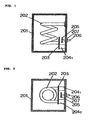
- Fig. 1 is a vertical cross section of a conventional helical resonator
- Fig. 2 is a horizontal cross section thereof.
- This helical resonator comprises an external conductor 201; a capacitor electrode 203; insulators 204 1 and 204 2 ; a helical resonance element 202 at one end mechanically fixed to and electrically connected with the inside wall of the external conductor 201 , wound coil-like in its middle portion, attached at the other end to the capacitor electrode 203 , and fixed to the inside wall of the external conductor 201 via the insulators 204 1 and 204 2 ; a movable electrode 205 ; a drive screw 206 to one end of which the movable electrode 205 is attached, and which passes through the external conductor 201 ; a lock nut 207 that is used to fix the drive screw 206 to the external conductor 201 ; and input/output coupling elements and input/output terminals (not shown)
- the resonance frequency can be finely tuned by rotating the drive screw 206 forward or backward to move the movable electrode 205 ahead or back so that the capacity of the electrode 203 can be varied.
- the conventional resonator described above has the following drawbacks.
- the helical resonance element 202 is formed by the winding of a metallic wire or a relatively thin rod-shaped conductor in the form of a coil, not only is the heat-radiating surface area of the helical resonance element 202 itself small, but the thermal conductivity into the external conductor 201 is poor, so the heat produced by power loss in the helical resonance element 202 is not effectively radiated from the helical resonance element 202 and the external conductor 201 , and the resonance frequency fluctuates as a result of distortion due to the elevated temperature of the various constituent components of the resonator.
- the ends of the helical resonance element 202 are directly or indirectly supported by and fixed to the inside wall of the external conductor 201, but the middle portion is not supported by any support, and is instead formed so that it maintains a coiled posture by its own rigidity, so vibration resistance is poor, fabrication is difficult, and the cost is high.
- a helical resonance element Because of its high impedance, a helical resonance element has inferior withstand voltage characteristics.
- CH-A-315 733 discloses a resonator comprising an outer cylindrical conductor and an inner cylindrical conductor. A first terminal is connected to the inner conductor, whereas a second terminal is connected to the outer conductor. The end portions of the inner and outer conductors are short circuited. The other end portions are connected to a capacity.
- the resonator according to the present invention comprises:
- a preferred embodiment of the resonator according to the present invention comprises a hollow cylinder composed of a solid dielectric whose upper and lower end portions face the upper and lower walls respectively, of the external conductor a suitable distance away, a first fixed electrode composed of a metal thin layer that adheres around the inner surface of the hollow cylinder and whose lower end portion is electrically connected to the lower wall of the external conductor, the second fixed electrode being composed of a metal thin layer that adheres around the outer surface of the hollow cylinder and whose upper end portion is electrically connected to the upper wall of the external conductor.
- the means for connecting the fixed electrode to the input terminal and the output terminal in a high-frequency fashion comprises two inductance elements or two capacity elements for the compensation of transmission characteristics connected in series between the input terminal and the output terminal; and the connecting point of the two inductance elements or the two capacity elements being connected to the second fixed electrode in a high-frequency fashion.
- a filter according to the present invention comprises:
- the resonator according to the present invention has good thermal conductivity between the capacitor element and the external conductor because of the relatively large thermal radiation surface area of the resonance capacity element, so heat is effectively radiated from the capacitor element and the external conductor, and therefore the rise in the temperature of the various resonator components is kept low and there is extremely little fluctuation in resonance frequency caused by distortion of the components as a result of elevated temperature. Furthermore, the structure is extremely simple and mechanically tough, so the product has excellent vibration resistance. The withstand voltage characteristics are also good because of the low impedance of the resonator.
- the range over which the capacity can be varied is wider and the resonance frequency can be set over a wider range, so resonators with a greater variety of resonance frequencies can be formed using parts of the same configurations and the same dimensions, and the costs entailed can therefore be lowered.
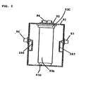
- Fig. 3 is a vertical cross section of the resonator according to the present invention
- Fig. 4 is a horizontal cross section thereof.
- the resonator in this embodiment comprises a cubic external conductor 91; a solid dielectric hollow cylinder 92 made of ceramic; a variable capacitor element composed of fixed electrodes 93A and 93B, and a movable electrode 94; a fixing member 93C that is used to fix the fixed electrode 93A, a fixing member 93D that is used to fix the fixed electrode 93B, a lock nut 95 that is used to fix the movable electrode 94; an input terminal 96; an output terminal 97; an input coupling wire 98; an output coupling wire 99; a resonance frequency fine-tuning element 100; and a lock nut 101.
- the external conductor 91 may also be a bottomed cylinder.
- the upper and lower ends of the hollow cylinder 92 are a suitable distance apart from, and face the upper and lower walls, respectively, of the external conductor 91.
- the fixed electrode 93A, 93B are made of a metal thin layer such as silver that is bonded around the inside and outside, respectively, of the hollow cylinder 92.
- the upper end of the fixed electrode 93A is soldered to the inner side of the conductive fixing member 93C, which is in the form of a flanged hollow cylinder, and the flange of the fixing member 93C is fixed by a screw to the upper wall of the external conductor 91.
- the lower end of the fixed electrode 93B is attached in elastic contact with the upper portion of the conductive fixing member 93D whose upper portion is provided with a plurality of slits to achieve elasticity and which is in the form of a bottomed hollow cylinder.
- This fixing member 93D is fixed to the lower wall of the external conductor 91 by a screw, using the threaded hole formed in the bottom of itself.
- the movable electrode 94 made of a solid or hollow cylindrical conductor (such as copper) threaded around its outside, and is screwed into the threaded hole formed in the upper wall of the external conductor 91 coaxially with the fixed electrodes 93A and 93B.
- the insertion length of the movable electrode 94 into the hollow cylinder 92, and therefore the insertion length of the movable electrode 94 into the fixed electrode 93B can be varied by the rotation of the movable electrode 94 in a forward or reverse direction to move the movable electrode 94 forward or backward.
- the movable electrode 94 is fixed by the lock nut 95.
- the input terminal 96 and the output terminal 97 consist, for example, of coaxial plugs, and the external conductor that forms these coaxial plugs is connected to the external conductor 91.
- the input coupling wire 98 is connected at one end to the internal conductor of the coaxial plug 96, and at the other end to the fixed electrode 93A.
- the output coupling wire 99 is connected at one end to the internal conductor of the coaxial plug 97, and at the other end to the fixed electrode 93A.
- the fine-tuning element 100 is made of a metal screw threaded into the wall of the external conductor 91, and is fixed by a lock nut 101.
- a parallel resonance circuit whose equivalent circuit is shown in Fig. 5, is formed by the distributed inductance of the external conductor 91 and the capacity of the variable capacitor element composed of the solid dielectric hollow cylinder 92, the fixed electrodes 93A and 93B, and the movable electrode 94.
- the symbol R represents the resonance circuit
- the symbol M 6R represents the input magnetic field coupling coefficient
- the symbol M R7 represents the output magnetic field coupling coefficient.
- the electromagnetic field distribution in this resonator will be such that the electric field vector is expressed by the solid arrowed line E in Fig. 3, the current by the solid arrowed line I in Fig. 3 , and the magnetic field by the broken line H in Fig. 4.
- this resonator is a low impedance type with good withstand voltage characteristics.
- the Q (Q u ) of the variable capacitor element consisting of the solid dielectric hollow cylinder 92, the fixed electrodes 93A and 93B, and the movable electrode 94 can be ignored.
- the electronic energy that can be accumulated in this resonator will correspond to the volume of the external conductor 91, and the resistance in the metal portion of this resonator can be kept extremely low, so that an extremely large unloaded Q can be obtained.
- FIG. 3 illustrates an example of a case in which tap coupling by the coupling wires 98 and 99 is used as means for coupling in high-frequency fashion the input terminal 96 with the fixed electrode 93A, and the output terminal 97 with the fixed electrode 93A
- means for capacitively coupling the input terminal 96 with the fixed electrode 93A via the capacity element 102 and means for capacitively coupling the output terminal 97 with the fixed electrode 93A via the capacity element 103 may also be used, as shown in Fig. 6
- probes 104 and 105 may be used as the input/output coupling means, as shown in Fig. 7.
- loops 106 and 107 may be used as the input/output, coupling means, as shown in Fig. 8.
- Figs. 6 through 8 correspond to the cross section of Fig. 4 viewed from below, omitting the lower side wall of external conductor 91, and hereinafter the same applies to Fig, 9 similar to Figs. 6 through 8.
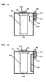
- Fig. 9 is a vertical cross section of the resonator of a further embodiment according to the present invention.
- a low-pass filter circuit is formed by inductance elements 108 and 109 for the compensation of transmission characteristics, interposed between the connection terminals 96 and 97 with the external circuit, and a capacity element 110 connected between the fixed electrode 93A that forms the capacitor element and the connection point of the inductance elements 108 and 109.
- Fig. 10 is an equivalent circuit diagram of the resonator shown in Fig. 9.
- the symbol R represents the resonance circuit composed of the external conductor 91 and the variable capacitor element, and the rest of the symbols are the same as in Fig. 9.
- the resonance frequency f 0 of the circuit composed of the resonance circuit R and the coupling-use capacity element 112 changes according to the capacitance of the coupling-use capacity element 110, and the fine tuning of the resonance frequency can be performed by the provision of an adjustment element similar to the resonance frequency fine-tuning element 100 shown in Fig. 4.
- Fig. 12 is a vertical cross section of the resonator of a further embodiment according to the present invention.
- This embodiment differs from the twelfth embodiment shown in Fig. 9 in that the coupling of the connection point of the inductance elements 108 and 109 with the fixed electrode 93A is performed by tap coupling using an inductance element 111, and in that the resonance frequency f 0 of the circuit composed of the resonance circuit R and the coupling-use inductance element 111 changes according to the inductance of the inductance element 111.
- the rest of the structure and operation is substantially the same as in the embodiment shown in Fig. 9.
- Fig. 13 is an equivalent circuit diagram of the resonator shown in Fig. 12. Except for the inductance element 111, all of the symbols are the same as in Fig. 10.
- Fig. 14 where the axis of abscissa and the axis of ordinate are the same as in Fig. 11, is a diagram illustrating the transmission characteristics of the resonator shown in Fig. 12, which is substantially the same as the characteristics shown in Fig. 11.
- Fig. 15 is a vertical cross section of the resonator of a further embodiment according to the present invention. This embodiment differs from the twelfth embodiment shown in Fig. 9 in that the inductance elements 108 and 109 used in the embodiment shown in Fig. 9 are replaced with capacity elements 112 and 113. The rest of the structure is the same as in the embodiment shown in Fig. 9.
- Fig. 16 is an equivalent circuit diagram of the resonator shown in Fig. 15. Except for the capacity elements 112 and 113, all of the symbols are the same as in Fig. 10.
- Fig. 17 where the axis of abscissa and the axis of ordinate are the same as in Fig. 11 , is a diagram illustrating the transmission characteristics of the resonator shown in Fig. 15.
- the slope of the attenuation characteristic curve in the frequency region lower than the resonance frequency f 0 is gentle, while the slope of the attenuation characteristic curve in the frequency region higher than the resonance frequency f 0 is steep, and a transmission inhibition band is formed in the frequency region including the resonance frequency f 0 .
- Fig. 18 is a vertical cross section of the resonator of a further embodiment according to the present invention.
- This embodiment is the same as the fourteenth embodiment shown in Fig. 16 in that the capacity elements 112 and 113 are used as transmission characteristic compensation elements, and is the same as the embodiment shown in Fig. 12 in that tap coupling is performed using the inductance element 111 as a coupling element.
- the rest of the structure is the same as in the embodiment shown in Fig. 15.
- Fig. 19 is an equivalent circuit diagram of the resonator shown in Fig. 18. Except for the inductance element 111, all of the symbols are the same as in Fig. 72.
- Fig. 20 where the axis of abscissa and the axis of ordinate are the same as in Fig. 17, is a diagram illustrating the transmission characteristics of the resonator shown in Fig. 18, which is substantially the same as the characteristics shown in Fig. 17.
- Figs. 21 through 24 are cross sections illustrating further embodiments of the present invention.
- the resonator in Fig. 21 has a probe 104 in place of the coupling element 110 shown in Fig. 9 ;
- the resonator in Fig. 22 has a loop 106 in place of the coupling element 110 shown in Fig. 9;
- the resonator in Fig. 23 has a probe 104 in place of the coupling element 110 shown in Fig. 15 ;
- the resonator in Fig. 80 has a loop 106 in place of the coupling element 110 shown in Fig. 15.
- the rest of the structure in the respective figs. are the same as the structure in Fig. 9 or 15.
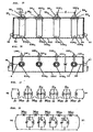
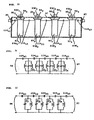
- Fig. 25 is a vertical cross section of a filter constructed using the resonator shown in Fig. 3, and Fig. 26 is a horizontal cross section thereof.
- This filter comprises an external conductor 91C; fixed electrodes 93A 1 through 93A 4 and 93B 1 through 93B 4 similar to the fixed electrodes 93A and 93B shown in Fig. 3 ; solid dielectric hollow cylinders 92 1 through 92 4 similar to the solid dielectric hollow cylinder 92 shown in Fig.
- fixing members 93C 1 through 93C 4 that are used to fix the fixed electrodes 93A 1 through 93A 4
- fixing members 93D 1 through 93D 4 that are used to fix the fixed electrodes 93B 1 through 93B 4
- variable electrodes 94 1 through 94 4 that make up the variable resonance capacity element along with the fixed electrodes 93A 1 through 93A 4 and 93B 1 through 93B 4 and are similar to the movable electrode 94 shown in Fig.
- lock nuts 95 1 through 95 4 that are used to fix the variable electrodes 94 1 through 94 4 ; an input terminal 96; an output terminal 97; an input coupling wire 98; an output coupling wire 99; resonance frequency fine-tuning elements 100 1 through 100 4 ; and lock nuts 101 1 through 101 4 that are used to fix the fine-tuning elements 100 1 through 100 4 .
- Fig. 27 is an equivalent circuit diagram of the filter shown in Figs. 25 and 26.
- Symbols R 1 through R 4 represent resonance circuits
- the symbol M 61 represents the input magnetic field coupling coefficient
- the symbol M 47 represents the output magnetic field coupling coefficient
- symbols M 12 through M 34 represent the interstage magnetic field coupling coefficients.
- Fig. 28 is a converted equivalent circuit diagram of the equivalent circuit diagram shown in Fig. 27, and the symbols are the same as in Fig. 27.
- Figs. 25 through 28 illustrate a case in which the input/output coupling elements are made of the tap coupling wires 98 and 99, a capacity coupling element made of the capacitors 102 and 103 or the probes 104 and 105 or a magnetic field coupling element made of the loops 106 and 107 shown in Figs. 5 through 8 may also be used to implement the present invention.
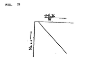
- Fig. 29 illustrates an example of the relation between the interstage magnetic field coupling coefficient and the center spacing of adjacent resonance capacity elements, obtained as a result of repeated experimentation with prototypes by the inventor.
- the axis of abscissa represents (d - 0.3C)/W where d is the center spacing of adjacent capacitor elements (see Fig. 25), C is the external diameter of the fixed electrodes 93A 1 through 93A 4 that form the variable capacitor element (see Fig. 25), and W is the width of the external conductor 91C (see Fig. 26).
- the axis of ordinate represent the interstage magnetic field coupling coefficient M k, k+1.
- Fig. 30 is a vertical cross section of a band-pass filter in which the interstage coupling consists of capacitive coupling.
- This filter comprises an external conductor 91C; fixed electrodes 93A 1 through 93A 4 , solid dielectric hollow cylinders 92 1 through 92 4 and fixed electrodes 93B 1 through 93B 4 that are provided concentrically to the interiors of the fixed electrodes 93A 1 through 93A 4 , although not shown in the Fig. 30 ; fixing members 93C 1 through 93C 4 ; fixing members 93D 1 through 93D 4 ; lock nuts 95 1 through 95 4 ; an input terminal 96; an output terminal 97 ; an input coupling capacity element 114 61 ; interstage coupling capacity elements 114 12 through 114 34 ; and an output coupling capacity element 114 47 .
- Fig. 31 is an equivalent circuit diagram of the band-pass filter shown in Fig. 30 .
- Symbols R 1 through R 4 represent resonance circuits
- the reference numeral 114 61 is the input coupling capacity
- reference numeral 114 12 through 114 34 represent the interstage coupling capacity
- the reference numerals 114 47 represent the output coupling capacity.
- Fig. 32 is a converted equivalent circuit diagram of the equivalent circuit diagram shown in Fig. 31, and the symbols are the same as in Fig. 31.
- Fig. 30 illustrates an example of a case in which the input/output coupling elements consist of capacity elements, tap coupling wires, probes, loops, or other such high-frequency coupling means may also be used.
- the fixed electrodes 93A and 93B can be constructed from a hollow cylinder made of a metal conductor that has been strengthened by making the walls thicker, and an air layer can be used instead of the hollow cylinder 92 made of a solid dielectric.
Landscapes
- Physics & Mathematics (AREA)
- Electromagnetism (AREA)
- Control Of Motors That Do Not Use Commutators (AREA)
Claims (4)
- Resonator, umfassend:dadurch gekennzeichnet, dass eine aus einem hohlen Metallzylinder zusammensetzte zweite Festelektrode (93A, 93A1-93A4) koaxial mit der ersten Festelektrode (93B) mit einem Spalt an der Außenseite der ersten Festelektrode (93B) bereitgestellt ist, und deren oberer Endteil an der oberen Wand des Außenleiters (91) befestigt ist, und dass Einrichtungen (98, 99) zum Anschluss der zweiten Festelektrode (93A, 93A1-93A4) am Eingabeanschluss (96) und Abgabeanschluss (97) auf Hochfrequenz-Art bereitgestellt sind.einen Außenleiter (91);ein variables Kondensator-Element, umfassend eine erste Festelektrode (93B), zusammengesetzt aus einem hohlen Metallzylinder, dessen unterer Endteil an der unteren Wand des Außenleiters (91) befestigt ist, und eine bewegliche hohle oder massive zylindrische Elektrode (94), welche mit der ersten Festelektrode (93B) koaxial und an der oberen Wand des Auβenleiters (91) so befestigt ist, dass die Einfügungslänge der beweglichen Elektrode (94) in die erste Festelektrode (93B) verändert werden kann; undeinen Eingabeanschluss (96) und einen Ausgabeanschluss (97);
- Resonator gemäß Anspruch 1, bei dem ein aus einem festen Dielektrum zusammengesetzter Hohzylinder (92) vorgesehen ist, deren oberer und unterer Endteil der oberen bzw. unteren Wand des Außenleiters (91) in einem geeigneten Abstand gegenüberliegen, wobei die erste Festelektrode (93B) aus einer dünnen Metallschicht zusammengesetzt ist, welche um die Innenfläche des Hohlzylinders (92) herum haftet, und deren unterer Endteil an die untere Wand des Außenleiters (91) elektrisch angeschlossen ist, und wobei die zweite Festelektrode (93 A, 93A1-93A4) aus einer dünnen Metallschicht zusammengesetzt ist, welche um die Außenfläche des Hohlzylinders (92) herum haftet, und deren oberer Endteil an die obere Wand des Außenleiters (91) elektrisch angeschlossen ist.
- Resonator gemäß Anspruch 1 oder 2, bei dem die Einrichtungen zum Verbinden der Festelektrode mit dem Eingabeanschluss und dem Ausgabeanschluss auf Hochfrequenz-Art zwei Induktivitätselemente (108, 109) oder zwei Kapazitätselemente (112, 113) zum Ausgleich der Übertragungscharakteristika umfasst, welche zwischen dem Eingabeanschluss (96) und dem Ausgabeanschluss (97) in Reihe angeschlossen sind, wobei der Anschlusspunkt der beiden Induktivitätselemente oder der beiden Kapazitätselemente an die zweite Festelektrode (93A) auf Hochfrequenz-Art angeschlossen ist.
- Filter, umfassend:einen Außenleiter (91C);eine Vielzahl variabler Kondensatorelemente (114) gemäß einem der Ansprüche 1 oder 2, die in Reihe auf Hochfrequenz-Art angeschlossen und in geeigneten Abständen bereitgestellt sind; undeine Vorrichtung (11461) zur Verbindung der zweiten Elektrode (93) des obersten Kondensator-Elements der Vielzahl von Kondensator-Elementen mit dem Eingabeanschluss (96) auf Hochfrequenz-Art, und eine Vorrichtung (11447) zur Verbindung der zweiten Festelektrode (93) des letzten Kondensator-Elements der Vielzahl von Kondensatorelementen mit dem Abgabeanschluss (97) auf Hochfrequenz-Art.
Applications Claiming Priority (10)
| Application Number | Priority Date | Filing Date | Title |
|---|---|---|---|
| JP6087807A JP2631268B2 (ja) | 1994-03-31 | 1994-03-31 | 共振器及びこの共振器より成るろ波器 |
| JP87807/94 | 1994-03-31 | ||
| JP8780794 | 1994-03-31 | ||
| JP28412494 | 1994-10-25 | ||
| JP284124/94 | 1994-10-25 | ||
| JP28412494A JPH08125405A (ja) | 1994-10-25 | 1994-10-25 | 共振器及びこの共振器より成るろ波器 |
| JP5197195 | 1995-02-15 | ||
| JP51971/95 | 1995-02-15 | ||
| JP5197195A JPH08222915A (ja) | 1995-02-15 | 1995-02-15 | 共振器及びこの共振器より成るろ波器 |
| PCT/JP1995/000629 WO1995027318A1 (en) | 1994-03-31 | 1995-03-31 | Resonator and filter using it |
Publications (3)
| Publication Number | Publication Date |
|---|---|
| EP0703634A1 EP0703634A1 (de) | 1996-03-27 |
| EP0703634A4 EP0703634A4 (de) | 1996-07-24 |
| EP0703634B1 true EP0703634B1 (de) | 2003-02-26 |
Family
ID=27294500
Family Applications (1)
| Application Number | Title | Priority Date | Filing Date |
|---|---|---|---|
| EP95913401A Expired - Lifetime EP0703634B1 (de) | 1994-03-31 | 1995-03-31 | Resonator und diesen verwendendes filter |
Country Status (7)
| Country | Link |
|---|---|
| US (1) | US5691675A (de) |
| EP (1) | EP0703634B1 (de) |
| KR (1) | KR100323895B1 (de) |
| CN (1) | CN1111923C (de) |
| DE (1) | DE69529715T2 (de) |
| FI (1) | FI115425B (de) |
| WO (1) | WO1995027318A1 (de) |
Families Citing this family (12)
| Publication number | Priority date | Publication date | Assignee | Title |
|---|---|---|---|---|
| FI110393B (fi) * | 1996-05-07 | 2003-01-15 | Solitra Oy | Suodatin |
| SE518119C2 (sv) * | 1996-12-20 | 2002-08-27 | Ericsson Telefon Ab L M | Resonansfilter med justerbar filtermekanism |
| SE513293C2 (sv) * | 1998-12-18 | 2000-08-21 | Ericsson Telefon Ab L M | Fästanordning vid kontaktövergång |
| US6404307B1 (en) | 1999-12-06 | 2002-06-11 | Kathrein, Inc., Scala Division | Resonant cavity coupling mechanism |
| US6329305B1 (en) | 2000-02-11 | 2001-12-11 | Agere Systems Guardian Corp. | Method for producing devices having piezoelectric films |
| SE527798C2 (sv) * | 2004-10-19 | 2006-06-07 | Powerwave Technologies Sweden | Ett DC-extraherande arrangemang |
| WO2012025946A1 (en) | 2010-08-25 | 2012-03-01 | Commscope Italy S.R.L. | Tunable bandpass filter |
| EP2882033A1 (de) * | 2013-12-09 | 2015-06-10 | Centre National De La Recherche Scientifique | Hochfrequenzresonator und Filter |
| US9755288B2 (en) * | 2014-09-29 | 2017-09-05 | Alcatel-Lucent Shanghai Bell Co., Ltd. | Methods and devices for integrating radio frequency and other signals within a conductor |
| WO2016164603A1 (en) * | 2015-04-07 | 2016-10-13 | Plasma Igniter, LLC | Radio frequency directional coupler and filter |
| WO2016174424A2 (en) * | 2015-04-28 | 2016-11-03 | David Rhodes | A tuneable microwave filter and a tuneable microwave multiplexer |
| CN111404510A (zh) | 2020-04-21 | 2020-07-10 | 安徽安努奇科技有限公司 | 谐振电路和滤波器件 |
Family Cites Families (16)
| Publication number | Priority date | Publication date | Assignee | Title |
|---|---|---|---|---|
| CH315733A (de) * | 1953-08-26 | 1956-08-31 | Patelhold Patentverwertung | Schwingsystem für Ultrakurzwellen |
| US4053856A (en) * | 1976-02-03 | 1977-10-11 | Fisher Sidney T | Quasi-toroidal inductor and resonator |
| JPS5535560A (en) * | 1978-09-04 | 1980-03-12 | Matsushita Electric Ind Co Ltd | Coaxial type filter |
| DE2947519C2 (de) * | 1979-11-24 | 1983-02-10 | Herfurth Gmbh, 2000 Hamburg | Schwingkreisanordnung |
| JPS6218963Y2 (de) * | 1980-01-11 | 1987-05-15 | ||
| JPS5879301A (ja) * | 1981-11-06 | 1983-05-13 | Mitsubishi Electric Corp | 高周波ろ波器 |
| JPS58105602A (ja) * | 1981-12-18 | 1983-06-23 | Fujitsu Ltd | 誘電体フイルタ |
| JPS5915304A (ja) * | 1982-07-15 | 1984-01-26 | Matsushita Electric Ind Co Ltd | 同軸型誘電体共振器 |
| FR2535547B1 (fr) * | 1982-10-29 | 1988-09-16 | Thomson Csf | Resonateurs bi-rubans et filtres realises a partir de ces resonateurs |
| US4614925A (en) * | 1983-07-05 | 1986-09-30 | Matsushita Electric Industrial Co., Ltd. | Resonator filters on dielectric substrates |
| JPS6014504A (ja) * | 1983-07-05 | 1985-01-25 | Matsushita Electric Ind Co Ltd | 同調器 |
| US4568985A (en) * | 1983-07-11 | 1986-02-04 | Datacopy Corporation | Electronic camera scanning mechanism |
| GB2163009B (en) * | 1984-08-10 | 1987-11-04 | Marconi Co Ltd | High-frequency electrical network |
| JPS6161503A (ja) * | 1984-08-31 | 1986-03-29 | Murata Mfg Co Ltd | 誘電体共振器 |
| JPH01103001A (ja) * | 1987-10-15 | 1989-04-20 | Murata Mfg Co Ltd | 誘電体フィルタ |
| SU1741200A1 (ru) * | 1989-05-11 | 1992-06-15 | Новосибирский электротехнический институт связи им.Н.Д.Псурцева | Перестраиваемый резонатор |
-
1995
- 1995-03-31 US US08/556,905 patent/US5691675A/en not_active Expired - Fee Related
- 1995-03-31 EP EP95913401A patent/EP0703634B1/de not_active Expired - Lifetime
- 1995-03-31 KR KR1019950705375A patent/KR100323895B1/ko not_active Expired - Fee Related
- 1995-03-31 CN CN95190422A patent/CN1111923C/zh not_active Expired - Fee Related
- 1995-03-31 DE DE69529715T patent/DE69529715T2/de not_active Expired - Fee Related
- 1995-03-31 WO PCT/JP1995/000629 patent/WO1995027318A1/ja not_active Ceased
- 1995-11-29 FI FI955759A patent/FI115425B/fi not_active IP Right Cessation
Also Published As
| Publication number | Publication date |
|---|---|
| KR960703278A (ko) | 1996-06-19 |
| FI955759A0 (fi) | 1995-11-29 |
| KR100323895B1 (ko) | 2002-06-24 |
| EP0703634A4 (de) | 1996-07-24 |
| EP0703634A1 (de) | 1996-03-27 |
| CN1111923C (zh) | 2003-06-18 |
| WO1995027318A1 (en) | 1995-10-12 |
| CN1128585A (zh) | 1996-08-07 |
| FI955759L (fi) | 1996-01-22 |
| US5691675A (en) | 1997-11-25 |
| DE69529715T2 (de) | 2003-09-11 |
| FI115425B (fi) | 2005-04-29 |
| DE69529715D1 (de) | 2003-04-03 |
Similar Documents
| Publication | Publication Date | Title |
|---|---|---|
| FI78198B (fi) | Oeverfoeringsledningsresonator. | |
| EP0703634B1 (de) | Resonator und diesen verwendendes filter | |
| JPS6161722B2 (de) | ||
| US6011516A (en) | Multiband antenna with a distributed-constant dielectric resonant circuit as an LC parallel resonant circuit, and multiband portable radio apparatus using the multiband antenna | |
| US3621484A (en) | Helical resonator having variable capacitor which includes windings of reduced diameter as one plate thereof | |
| US3936776A (en) | Interspersed double winding helical resonator with connections to cavity | |
| US4184123A (en) | Double-tuned output circuit for high power devices using coaxial cavity resonators | |
| US2892163A (en) | Band-pass filters | |
| US4626862A (en) | Antenna having coaxial driven element with grounded center conductor | |
| US3448412A (en) | Miniaturized tunable resonator comprising intermeshing concentric tubular members | |
| KR100249838B1 (ko) | 유자형 공진기를 갖는 고주파 필터 | |
| US5576673A (en) | Small, low-pass filter for high power applications | |
| JP2655133B2 (ja) | 共振器及びこの共振器より成るろ波器 | |
| US4075583A (en) | Low loss tuneable filter | |
| EP0443173B1 (de) | Durchstimmbarer monolithischer Breitbandinduktor | |
| JPH0618640A (ja) | 核磁気共鳴検出器 | |
| KR20050036522A (ko) | 공진기 노치 필터 | |
| JP5519947B2 (ja) | 帯域通過フィルタ | |
| JPH06188607A (ja) | ノッチフィルタ及びこのノッチフィルタを用いて成るノッチダイプレクサ | |
| US3098206A (en) | Wave band uhf output network | |
| JP3428928B2 (ja) | 帯域内群遅延一定型誘電体フィルタとそれを用いた歪み補償型増幅器 | |
| JP2631268B2 (ja) | 共振器及びこの共振器より成るろ波器 | |
| JPH08222915A (ja) | 共振器及びこの共振器より成るろ波器 | |
| JPH11214905A (ja) | 共振器及びこの共振器を用いたフィルタ | |
| JP3050538B2 (ja) | 群遅延時間補償形帯域通過フィルタ |
Legal Events
| Date | Code | Title | Description |
|---|---|---|---|
| PUAI | Public reference made under article 153(3) epc to a published international application that has entered the european phase |
Free format text: ORIGINAL CODE: 0009012 |
|
| AK | Designated contracting states |
Kind code of ref document: A1 Designated state(s): DE FR GB SE |
|
| 17P | Request for examination filed |
Effective date: 19960410 |
|
| A4 | Supplementary search report drawn up and despatched | ||
| AK | Designated contracting states |
Kind code of ref document: A4 Designated state(s): DE FR GB SE |
|
| RHK1 | Main classification (correction) |
Ipc: H01P 1/20 |
|
| 17Q | First examination report despatched |
Effective date: 19990527 |
|
| GRAH | Despatch of communication of intention to grant a patent |
Free format text: ORIGINAL CODE: EPIDOS IGRA |
|
| GRAH | Despatch of communication of intention to grant a patent |
Free format text: ORIGINAL CODE: EPIDOS IGRA |
|
| GRAA | (expected) grant |
Free format text: ORIGINAL CODE: 0009210 |
|
| RAP1 | Party data changed (applicant data changed or rights of an application transferred) |
Owner name: NIHON DENGYO KOSAKU CO. LTD. |
|
| AK | Designated contracting states |
Designated state(s): DE FR GB SE |
|
| REG | Reference to a national code |
Ref country code: GB Ref legal event code: FG4D |
|
| REF | Corresponds to: |
Ref document number: 69529715 Country of ref document: DE Date of ref document: 20030403 Kind code of ref document: P |
|
| REG | Reference to a national code |
Ref country code: SE Ref legal event code: TRGR |
|
| ET | Fr: translation filed | ||
| PLBE | No opposition filed within time limit |
Free format text: ORIGINAL CODE: 0009261 |
|
| STAA | Information on the status of an ep patent application or granted ep patent |
Free format text: STATUS: NO OPPOSITION FILED WITHIN TIME LIMIT |
|
| 26N | No opposition filed |
Effective date: 20031127 |
|
| PGFP | Annual fee paid to national office [announced via postgrant information from national office to epo] |
Ref country code: SE Payment date: 20060208 Year of fee payment: 12 |
|
| PGFP | Annual fee paid to national office [announced via postgrant information from national office to epo] |
Ref country code: GB Payment date: 20060302 Year of fee payment: 12 |
|
| PGFP | Annual fee paid to national office [announced via postgrant information from national office to epo] |
Ref country code: FR Payment date: 20060327 Year of fee payment: 12 |
|
| PGFP | Annual fee paid to national office [announced via postgrant information from national office to epo] |
Ref country code: DE Payment date: 20060526 Year of fee payment: 12 |
|
| GBPC | Gb: european patent ceased through non-payment of renewal fee |
Effective date: 20070331 |
|
| REG | Reference to a national code |
Ref country code: FR Ref legal event code: ST Effective date: 20071130 |
|
| PG25 | Lapsed in a contracting state [announced via postgrant information from national office to epo] |
Ref country code: DE Free format text: LAPSE BECAUSE OF NON-PAYMENT OF DUE FEES Effective date: 20071002 |
|
| PG25 | Lapsed in a contracting state [announced via postgrant information from national office to epo] |
Ref country code: GB Free format text: LAPSE BECAUSE OF NON-PAYMENT OF DUE FEES Effective date: 20070331 |
|
| PG25 | Lapsed in a contracting state [announced via postgrant information from national office to epo] |
Ref country code: SE Free format text: LAPSE BECAUSE OF NON-PAYMENT OF DUE FEES Effective date: 20070401 |
|
| PG25 | Lapsed in a contracting state [announced via postgrant information from national office to epo] |
Ref country code: FR Free format text: LAPSE BECAUSE OF NON-PAYMENT OF DUE FEES Effective date: 20070402 |