EP0704732B1 - Integrierter optoelektronischer Verbund und Stecker - Google Patents
Integrierter optoelektronischer Verbund und Stecker Download PDFInfo
- Publication number
- EP0704732B1 EP0704732B1 EP95306828A EP95306828A EP0704732B1 EP 0704732 B1 EP0704732 B1 EP 0704732B1 EP 95306828 A EP95306828 A EP 95306828A EP 95306828 A EP95306828 A EP 95306828A EP 0704732 B1 EP0704732 B1 EP 0704732B1
- Authority
- EP
- European Patent Office
- Prior art keywords
- submount
- substrate
- base
- coupler
- array
- Prior art date
- Legal status (The legal status is an assumption and is not a legal conclusion. Google has not performed a legal analysis and makes no representation as to the accuracy of the status listed.)
- Expired - Lifetime
Links
Images


Classifications
-
- G—PHYSICS
- G02—OPTICS
- G02B—OPTICAL ELEMENTS, SYSTEMS OR APPARATUS
- G02B6/00—Light guides; Structural details of arrangements comprising light guides and other optical elements, e.g. couplings
- G02B6/24—Coupling light guides
- G02B6/42—Coupling light guides with opto-electronic elements
- G02B6/4201—Packages, e.g. shape, construction, internal or external details
- G02B6/4204—Packages, e.g. shape, construction, internal or external details the coupling comprising intermediate optical elements, e.g. lenses, holograms
- G02B6/421—Packages, e.g. shape, construction, internal or external details the coupling comprising intermediate optical elements, e.g. lenses, holograms the intermediate optical component consisting of a short length of fibre, e.g. fibre stub
-
- G—PHYSICS
- G02—OPTICS
- G02B—OPTICAL ELEMENTS, SYSTEMS OR APPARATUS
- G02B6/00—Light guides; Structural details of arrangements comprising light guides and other optical elements, e.g. couplings
- G02B6/24—Coupling light guides
- G02B6/42—Coupling light guides with opto-electronic elements
- G02B6/4201—Packages, e.g. shape, construction, internal or external details
- G02B6/4249—Packages, e.g. shape, construction, internal or external details comprising arrays of active devices and fibres
-
- G—PHYSICS
- G02—OPTICS
- G02B—OPTICAL ELEMENTS, SYSTEMS OR APPARATUS
- G02B6/00—Light guides; Structural details of arrangements comprising light guides and other optical elements, e.g. couplings
- G02B6/24—Coupling light guides
- G02B6/42—Coupling light guides with opto-electronic elements
- G02B6/4201—Packages, e.g. shape, construction, internal or external details
- G02B6/4219—Mechanical fixtures for holding or positioning the elements relative to each other in the couplings; Alignment methods for the elements, e.g. measuring or observing methods especially used therefor
- G02B6/4228—Passive alignment, i.e. without a detection of the degree of coupling or the position of the elements
- G02B6/423—Passive alignment, i.e. without a detection of the degree of coupling or the position of the elements using guiding surfaces for the alignment
- G02B6/4231—Passive alignment, i.e. without a detection of the degree of coupling or the position of the elements using guiding surfaces for the alignment with intermediate elements, e.g. rods and balls, between the elements
-
- G—PHYSICS
- G02—OPTICS
- G02B—OPTICAL ELEMENTS, SYSTEMS OR APPARATUS
- G02B6/00—Light guides; Structural details of arrangements comprising light guides and other optical elements, e.g. couplings
- G02B6/24—Coupling light guides
- G02B6/42—Coupling light guides with opto-electronic elements
- G02B6/4201—Packages, e.g. shape, construction, internal or external details
- G02B6/4219—Mechanical fixtures for holding or positioning the elements relative to each other in the couplings; Alignment methods for the elements, e.g. measuring or observing methods especially used therefor
- G02B6/4228—Passive alignment, i.e. without a detection of the degree of coupling or the position of the elements
- G02B6/4232—Passive alignment, i.e. without a detection of the degree of coupling or the position of the elements using the surface tension of fluid solder to align the elements, e.g. solder bump techniques
-
- G—PHYSICS
- G02—OPTICS
- G02B—OPTICAL ELEMENTS, SYSTEMS OR APPARATUS
- G02B6/00—Light guides; Structural details of arrangements comprising light guides and other optical elements, e.g. couplings
- G02B6/24—Coupling light guides
- G02B6/42—Coupling light guides with opto-electronic elements
- G02B6/4201—Packages, e.g. shape, construction, internal or external details
- G02B6/4219—Mechanical fixtures for holding or positioning the elements relative to each other in the couplings; Alignment methods for the elements, e.g. measuring or observing methods especially used therefor
- G02B6/4236—Fixing or mounting methods of the aligned elements
- G02B6/4238—Soldering
-
- G—PHYSICS
- G02—OPTICS
- G02B—OPTICAL ELEMENTS, SYSTEMS OR APPARATUS
- G02B6/00—Light guides; Structural details of arrangements comprising light guides and other optical elements, e.g. couplings
- G02B6/24—Coupling light guides
- G02B6/42—Coupling light guides with opto-electronic elements
- G02B6/4292—Coupling light guides with opto-electronic elements the light guide being disconnectable from the opto-electronic element, e.g. mutually self aligning arrangements
-
- H—ELECTRICITY
- H10—SEMICONDUCTOR DEVICES; ELECTRIC SOLID-STATE DEVICES NOT OTHERWISE PROVIDED FOR
- H10W—GENERIC PACKAGES, INTERCONNECTIONS, CONNECTORS OR OTHER CONSTRUCTIONAL DETAILS OF DEVICES COVERED BY CLASS H10
- H10W72/00—Interconnections or connectors in packages
- H10W72/50—Bond wires
- H10W72/531—Shapes of wire connectors
- H10W72/536—Shapes of wire connectors the connected ends being ball-shaped
-
- H—ELECTRICITY
- H10—SEMICONDUCTOR DEVICES; ELECTRIC SOLID-STATE DEVICES NOT OTHERWISE PROVIDED FOR
- H10W—GENERIC PACKAGES, INTERCONNECTIONS, CONNECTORS OR OTHER CONSTRUCTIONAL DETAILS OF DEVICES COVERED BY CLASS H10
- H10W72/00—Interconnections or connectors in packages
- H10W72/50—Bond wires
- H10W72/531—Shapes of wire connectors
- H10W72/5363—Shapes of wire connectors the connected ends being wedge-shaped
Definitions
- This invention relates generally to the field of optoelectronics and more specifically is directed to an integrated coupler for coupling laser diodes or photodetectors to optical fibers.
- Optical interconnection of electronic data and communication systems is of great interest as it offers use of small, relatively lightweight cable, large transmission capacity, long transmission distance, and immunity to electromagnetic noise, compared with electrical cables using metallic conductors.
- Potential applications include, but are by no means limited to, telephone transmission lines, subscriber television cable service, and interconnection of subsystems in large computer architectures at different packaging hierarchies, such as chip-to-chip, board-to-board, card-cage to card-cage, and inter-cabinet connections.
- Optical fibers are continuous lengths of finely drawn, highly transparent glass material which can transmit light over long distances.
- Optical fibers must be interfaced to the electronic circuits which generate and process the electrical signals carried by the fibers.
- the electronic circuits drive light emitting semiconductors, such as laser diodes, which produce light pulses fed into the optical fibers.
- the light signals carried by the optical fibers are directed onto photodetectors which convert the optical, i.e. light signals to an electrical signal for further processing by electronic receiver circuitry.
- optical fiber transmission lines are made up of bundles of such fibers for carrying parallel data.
- Data is fed to each optical fiber by a corresponding light emitting element which is electrically modulated such that the light output corresponds to an electrical signal input.
- the light emitting elements are typically formed on a single semiconductor chip, such as a laser diode array, which may for example have twelve mutually independent laser diode emitters spaced along a line on a common face of the chip.
- the individual laser diodes of the array are closely spaced to each other and each emits a cone of light. The cones spread out and begin to overlap at a short distance from the laser chip.
- the laser diode emitters In order to avoid cross-over and interference between the optical signals, the laser diode emitters must be positioned closely to the end faces of the optical fibers comprising the optical transmission link.
- the close spacing between the laser diode emitters, coupled with the small diameter of the fiber end faces and even smaller core diameters, requires precise alignment of the diode array in relation to the optical fiber holder, so that a maximum amount of laser light illuminates the corresponding optical fiber core. Misalignment between the laser diode and the fiber core results in wasted laser output and a consequent weakening of the transmitted light signal.
- Proper alignment of the laser diode array is specially important when single mode optical fibers are employed, due to the very small diameter of the core of such fibers. Multi-mode optical fiber cores are substantially larger in diameter, and alignment of the laser diode array is easier in such case.
- improvement is needed in the packaging of the optoelectronic components, particularly the assemblies used for creating the interface between the electrical and optical portions of the system.
- improvement is needed in regard to the mounting of the light emitting and photo detector devices and their coupling to the optical fibers in order to improve the efficiency and reliability of the optoelectronic interconnects, and to reduce the cost of current assemblies which rely on discrete, precision machined components, require costly, labor intensive active alignment, and offer inadequate thermal and mechanical stability.
- One type of widely used optical fiber connector has an optical fiber holder where the fibers are captive in channels defined between an upper substrate and a lower substrate.
- one substrate has a surface traversed by parallel grooves, each groove having a V-shaped cross-section.
- a flat surface of the other substrate is joined against the grooved surface to define between the two substrates parallel channels of triangular cross-section.
- a fiber ribbon or cable containing one or more optical fibers is clamped between the two substrates and individual fibers extend from the cable or ribbon within corresponding channels and terminate at a common plane surface defined by the two substrates, the fiber ends being arranged along a straight line formed by the junction of the two substrates.
- Each optical fiber has a light transmitting core surrounded by a cladding.
- the diameter of the fiber is normally 125 microns including the cladding.
- the core diameter is 62.5 microns for multi-mode fibers, and only 10 microns for single mode fibers.
- the interior dimensions of the triangular channels are held to very close tolerances so that in cross section the cylindrical fibers make tangential contact with the center of each side surface of the channel.
- the fiber ends as well as the common plane surface of the substrates are highly polished and flat to facilitate close physical contact with a second similar holder for making an optical connection between two lengths of fiberoptic cable. Alignment of the fiber ends between the two connectors is ensured by precisely machined guide pins on one connector mated to equally precise guide holes in the other connector.
- This type of optical fiber connector is available from NGK of Japan with the two substrates made of ceramic material, and in a precision plastic version from US Conec Ltd., of Hickory, North Carolina.
- the optical alignment between the light emitting device and the optical fibers can be affected, diminishing the power delivered by the light emitting device to the optical fibers and in extreme cases disrupting the optoelectronic link.
- the invention disclosed below addresses the aforementioned need by providing an optoelectronic coupler featuring integrated, optically coupled mounting of a light emitting devices/photodetectors and optical fibers.
- the light emitting devices include light emitting semiconductors such as laser diodes.
- the photodetectors include photodiodes.
- an integrated coupler as set out in claim 1.
- the base, the substrate and the submount may be of the same material.
- the presently preferred material is non-metal inorganic materials, and in particular ceramics or glasses.
- ceramics may preferably be alumina, zirconia or a glass ceramics.
- other materials are also suitable such as dimensionally and thermally stable engineering plastics.
- the materials constituting the base, the substrate and the submount are in any case preferably selected so that the differences between the thermal expansion coefficients of the materials is not larger than 2.0 ⁇ 10 -6 /°C for improving thermal and mechanical stability of the integrated mounting.
- the light emitting devices when need in the invention may consist of multiple devices packaged as an array, in which case the array may have one common electrode of one polarity and a number of discrete electrodes of opposite polarity.
- Supply electrode pads can be provided on the substrate by selective metallization of the substrate surface.
- the array may be fixed to the submount by soldering the common electrode to a corresponding supply electrode pad on the submount and connecting the discrete electrodes by wire bonding to discrete supply electrode pads on the submount.
- the discrete electrodes of the array may be soldered to corresponding electrode pads on the submount, and the common electrode wire bonded to a corresponding supply electrode pad on the submount.
- bump pad soldering may be used where the surface tension of molten solder between the light emitting device or photodetecting device and the electrode pads on the submount brings the device into a realigned position, such that upon proper assembly of the submount to the base, the device will be correctly aligned with the cores of the optical fibers in the holder.
- the device can be positioned on the substrate in relation to reference pre-set reference markings. Either of these array mounting and positioning methods may be employed where the submount is integral with the base and the array is mounted directly to the base. Whether the submount is a separate element or is integral with the base, it serves to raise the array to a position where the array is in a common plane with the ends of the optical fibers.
- the light emitting device or photodetecting device array mounted to a separate submount can be assembled to the coupler and aligned with the optical fibers with the aid of guide pins positioned by means of pin guides accurately defined in the coupler.
- a pair of parallel guide pins inserted in the pin guides can be accurately positioned relative to the base and used as a reference for positioning the submount on the base with the array mounted on the submount in optical alignment with the optical fiber ends.
- the guide pins are removed once the submount and the array is assembled to the base.
- the pin guides may also serve to receive the pins of a male connector in one configuration of the coupler unit.
- an optical scrambler unit may also be integrated with the integrated mounting assembly and interposed between the light emitting device array or photodetecting device array and the first fiber ends.
- the scrambler unit is desirably made of the same material as the fiber holder and the base for thermal and mechanical compatibility.
- the scrambler unit can be constructed analogously to the optical fiber holder, by joining a V-grooved upper substrate to a plane surface of a lower substrate.
- the scrambler may be a single block of transparent material with integrally formed lens elements.
- a transparent ceramic may be used for this purpose, and the same ceramic also used for making the optical fiber holder, base and submount components of the integrated holder.
- the integrated coupler can be connected to a fiber optic cable by providing male or female retainers as the connector means configured to interlock with a connector of opposite gender at the end of the fiber optic cable, such that the connector normally attached to the tail is also integrated to the coupler which then combines the functions of on optoelectronic coupler and connector in one compact and rugged package. Airtight mechanical sealing and EMI shielding of an optoelectronic package are readily possible using such an integrated coupler by metallizing the coupler surfaces and sealing the fiber containing channels.
- the substrate and the base may be positioned to each other so that the side of the substrate parallel to the channels and the side of the base parallel to the channels form a common plane.
- the position of the substrate relative to the base may be determined accurately in a direction perpendicular to the channel.
- the submount may be mechanically positioned so that a distance between the side of the submount parallel to the channel and the above common surface is made constant.
- the position of the submount relative to each channel in a direction perpendicular to the channel may be determined accurately.
- Such accurate positioning may be carried out by using accurately machined base, submount and optical fiber holder each manufactured by NGK INSULATORS, LTD. as described below.
- the light emitting device array or photodetecting device array may be positioned accurately relative to the submount so that each light emitting device or photodetecting device may be positioned accurately relative to the corresponding channel and fiber in the channel without the active alignment described above.
- One side of the substrate at which the channels are open and the side of the base perpendicular to the channel may be positioned to each other so that they form a common plane.
- the substrate and the base may be accurately positioned to each other in a direction parallel to the channel.
- the submount and the base may be positioned to each other so that the rear edge of the submount on the opposite side of the front edge opposing to the substrate and the rear side of the base form a common plane.
- the base and the submount may be accurately positioned to each other in a direction parallel to the channel.
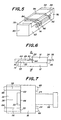
- Figure 1 shows an integrated optoelectronic coupler 10 which has a rectangular base 12 and an optical fiber holder 14 which includes a V-groove substrate 16 and a fiber clamping substrate 18, the assembly of which is better understood by reference to Figures 2 and 8.
- the upper, grooved substrate 16 has a number of parallel grooves 20 which extend fully across the upper substrate 16 between a front side 22 and a rear side 24.
- the upper substrate 16 also defines two parallel pin guide slots 26 with the upper surface 28 of the base 12.
- a laser diode array 30 is fixed to the top surface 33 of a submount 32 which in turn is fixed to the upper surface 28 of the base 12.
- Each groove 20 has a V-shaped cross-section, with two side walls in the groove at a 60 degree angle to each other.
- the top surface 34 of the lower substrate 18 covers the grooves 20, which then form parallel channels 36 of triangular cross-section extending between the opposite sides 22, 24 of the upper substrate 16.
- Each channel has an equilateral triangular cross-section such that a cylindrical optical fiber 40 laid within each groove 20 touches the center of each side wall of the triangular channels, making line contact with each side wall along the length of the channel.
- Each fiber 40 is thus closely contained in a straight line between the upper substrate 16 and lower substrate 18 which together form an optical fiber holder assembly.
- the optical fibers 40 extend from a fiber ribbon 38 clamped between the holder substrates 16 and 18.
- Each fiber 40 terminates at a fiber end face 68 which is polished flat with the front surface 22 of the V-grooved substrate 16.
- the upper substrate 16 and lower substrate 18 are made to very close tolerances by precision machining, as exemplified by the high precision ceramic optical multi-fiber connectors sold by NGK of Japan, through their U.S. distributors NGK-Locke, Inc. of Santa Clara, California.
- the NGK ceramic components features V-grooved substrates for supporting optical fibers in multi-fiber connectors and related assemblies.
- the existing NGK ceramic holders for optical fibers have a lower substrate or base which is of equal width as the width of the upper substrate 16 between its opposite sides 22, 24. It is an improvement to extend the base 12 beyond the front side 22 of the upper substrate 16, also support the submount 32 on a common base 12 with the V-grooved substrate 16, as shown in Figures 1 and 2.
- a side 93 of the substrate 16 parallel to each channel and a side 91 of the base 12 parallel to the channel are positioned to each other so that the sides 93 and 91 form a common plane.
- one side 24 of the substrate 16 at which the channels are opened and a side of the base 12 perpendicular to the channel are positioned to each other so that the side 24 and the side of the base 12 form a common plane.
- the laser diode array 30 has a number light emitting, lasing semiconductor junctions spaced along an active surface 44. Each lasing junction can be powered to emit a cone 46 of cohering light, only two of which are shown in the drawing. Each lasing junction has a corresponding electrode 48 in the form of a metallic pad deposited on the top side of the diode array. A common electrode on the hidden underside of the diode array 30 is soldered to and in electrical contact with a supply electrode 50 formed by surface metallization of the submount 32. Each of the discrete electrodes 48 is connected by wire bonding 52 to a respective supply electrode pads 54 on the substrate surface 33. Electrical power is supplied by a suitable contact arrangement, not shown in the drawings, to the electrode pads 50, 54 for powering the diode array 30.
- Figure 4 shows an alternate mounting of the laser diode 30 to the substrate 32 by the so called "flip-chip" or bump pad mounting.
- the diode array 30 is turned over and the discrete electrode pads 48 are directly bonded by soldering to corresponding supply electrodes 54' deposited on the submount surface 33.
- the common electrode 56 now on the top side of the laser diode 30, is wire bonded at 58 to a corresponding supply electrode 50'.
- the substrate 32, with the laser diode array 30 premounted on its top surface 33, is then bonded to the upper surface 28 of the common base 12, to make up the integrated optoelectronic coupler 10.
- the integrated coupler 10 provides an interface and transition between an electronic circuit where signals are carried by metallic conductors, to an optical transmission line made up of one or more optical fibers.
- alignment of the laser diode array 30 is accomplished by first referencing the position of the array 30 to the submount 32, and then referencing the position of the submount to the V-grooved upper substrate 16.
- Existing manufacturing technology in particular as implemented by the NGK company mentioned earlier, permits the manufacture of the upper substrate 16 with a high degree of dimensional accuracy.
- the submount 32 is likewise machined to close tolerances.
- the diode array 30 is mounted to the submount 30 at a known location, normally the center, between two opposite sides of the submount, specifically between side 56 and its opposite side 58.
- the precise-positioning of the laser array 30 in Figure 3 is accomplished by positioning the array 30 between reference markings 60a and 60b which are accurately placed on the submount 32 by measurement relative to the sides 56, 58.
- the active face 44 of the diode array is aligned against the front edge 62 of the submount. This positioning of the diode array 30 on the submount 32 is done on a heated stage of an assembly microscope which melts solder preapplied to the supply electrode 50 and on the common electrode on the underside of the diode array 30.
- the solder While heated, the solder remains fluid and allows the diode array 30 to be accurately positioned between the reference markings 60a, 60b and against the submount edge 62. once properly positioned, the solder is allowed to cool, or is actively cooled by a cooling system on the microscope stage, thereby fixing the diode array device to the substrate 32.
- Figure 4 shows an alternate approach for accurately referencing the diode array 30 in relation to the opposite sides 56, 58 of the submount 32.
- the supply electrode pads 54' are precisely positioned on the submount surface 33 by means of a photolithographic process in relation to the sides 56, 58.
- the discrete electrode pads 48 of the diode array 30 are dimensioned to match the width of the supply electrodes pads 54'.
- the submount 32 is placed on a heated assembly stage, with the diode array 30 positioned so that the discrete electrode pads 48 each overlie a corresponding supply electrode pad 54'. Preapplied solder on pads 48, 54' melts under the heating, creating a fluid film between the overlying pads 48, 54'.
- the molten solder exhibits substantial surface tension which tends to pull the diode array 30 into alignment with the submount pads 54', thereby correctly positioning the diode array 30 with reference to the sides 56, 58.
- the diode array 30 is also manually aligned against the front edge 62 of the submount 32, as explained in connection with Figure 3.
- the use of surface tension of the molten solder to align a semiconductor chip on a substrate provided with contact pads is known in the industry as "bump pad" mounting, and is known technique.
- the submount 32 is then mounted to the base 12 in alignment with the V-grooved substrate 16 with the aid of parallel guide pins 64 inserted through the pin guides 26.
- the two guide pins 64 are precisely dimensioned cylindrical pins which make a close sliding fit in the pin guide 26.
- the rear ends 66 of the guide pins may be fixed in a suitable holder (not shown in the drawings) which support the guide pins in mutually parallel and precisely spaced apart relationship, matching the spacing between the pin guide 26.
- the guide pins 64 are inserted through the pin guide 26 as shown in Figures 6 through 8, and rest upon the upper surface 28 of the base 12.
- the submount 32 with the laser diode array 30 premounted to it, is then assembled to the base 12.
- the submount 32 is placed on the base surface 28 between the guide pins 64.
- the width of the submount between its opposite surfaces 56, 58 is precisely matched, during its manufacture, to the spacing between the guide pins 64.
- the submount 32 therefore fits precisely between the two pins 64 on the base surface 28, thereby positioning the laser diodes of the array 30 in optical alignment with the end faces 68 of the optical fibers 40.
- the submount is positioned so that a distance between the side 92 (refer to Figure 1) of the submount parallel to the channel and the common plane formed by the sides 91, 93 is made constant, by means of said pins and pinguides.
- the submount 32 and the base 12 are positioned to each other so that the rear edge 70 of the submount 32 and the rear side 72 of the base 12 form a common plane.
- the substrate and the base are positioned to each other so that one side of the submount at which the channels are opened and the side of the base 12 perpendicular to the channel form a common plane.
- the integrated optoelectronic coupler 10 avoids the need for active alignment of the laser diode array 30 to the optical fibers 40, by using precise manufacturing and machining methods currently known and practiced in the industry in combination with novel coupler structures and assembly procedures.
- the gap spacing between the active, light emitting face 44 of the laser diode array and the end faces 40 of the optical fibers is fixed by the width dimension of the substrate 32 measured between its front edge 62 and rear edge 70, the latter being aligned with the rear side 72 of the base 12.
- the preferred material for use in making the submount 32 is the same material used for the V-grooved substrate 16 and the base 12.
- optical fibers 40 are currently commercially marketed by the aforementioned NGK Company which have an upper substrate 16 machined as needed for use in the present invention, and include a base portion which differs from the base 12 in the drawings only in that it terminates flush with the front surface 22 of the substrate 16.
- a common base for supporting the laser array as well as the fiber holder is provided.
- the substrate 16 and the submount 32 are mounted on a common extended base 12 which has been enlarged to accommodate the submount 32.
- the submount 32 has been described as a separate element from the base 12, but can also be made integrally with the base, eliminating the need for precise positioning of the submount relative to the base.
- the laser array can then be mounted directly to the integral submount by any of the procedures just described for its mounting to the separate submount.
- the integrated coupler 10 offers homogeneity of structural materials, thereby avoiding the thermal instabilities inherent in previous optoelectronic couplers and connectors.
- the use of ceramic throughout the structure of the coupler 10 assures a high degree of mechanical strength and dimensional stability due to the advantageous mechanical properties of ceramic materials.
- the result is a compact and rugged optoelectronic coupler which may be expected to perform dependably in commercial applications and which can be manufactured, assembled and aligned economically in commercial quantities.
- the need for active alignment of the coupler is eliminated, thereby substantially reducing the cost of manufacture.
- the integrated coupler 10 is equally suitable for use with an optoelectronic receiving package by substituting a photodetector for the laser diode array 30.
- a photodetector array 74 is fixed to a front surface 76 of a photodetector submount 78.
- the photodetector array 74 is fixed by soldering a common electrode on the hidden underside of the array chip to the metallized surface 82 of the submount 78, which metallized surface also serves as a supply electrode of one polarity.
- Power of the opposite polarity is supplied by supply electrodes 84 formed on the submount 78 and wire bonded to corresponding individual electrodes 86 for each photodetector element of the array.
- the alignment of the photodetector array 74 relative to optical fibers 40 on the integrated coupler 10 is obtained in a manner analogous to that described for the laser diode array 30 in Figure 3.
- the alignment of photodetectors is less difficult and less critical than for laser diode arrays. Consequently, the detector array 74 can be positioned on the submount 78 by reference to preset markings or features on the submount, such as the electrode pads 84, and metallization edge 88.
- the dimension between opposite sides 90 and 92 is closely matched to the spacing between the guide pins 64 in Figures 6 through 8, and submount 78 is assembled to the base 12 of the coupler 10 in the manner previously described in connection with the submount 32 of the laser diode array.
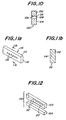
- an integrated optoelectronic coupler 10' embodying the present invention is shown which differs from the coupler 10 of Figures 1 through 8 in that an optical scrambler unit 100 has been interposed between the laser diode array 30 and the end faces 68 of the optical fibers held by the V-grooved substrate 16.
- the scrambler unit is made up of two elements, as shown in Figure 12, an upper V-grooved substrate 102 and a lower substrate 104 which are joined together as shown in the phantom lined and solid lined depictions of the scrambler unit 100 in Figure 9.
- the two substrates 102, 104 define between them a number of passages each having a triangular cross-section which matches the triangular cross-section of the channels containing the optical fibers between the lower substrate 18 and upper substrate 16 of the coupler.
- the scrambler is manufactured by the same methods and using the same materials as for the V-grooved substrate 16.
- the upper substrate 102 of the scrambler can be obtained by simply slicing a V-grooved substrate 16, thereby precisely matching the triangular channels of the fiber holder assembly, while the lower substrate 104 can be simply a rectangular block of the same material.
- the assembled scrambler unit 100 can be aligned with the triangular channels containing the optical fibers by inserting guide segments of optical fiber or rigid pins of the same diameter as the fibers through the triangular channels 106 of the scrambler unit and into the triangular channels of the optical fiber holder, i.e. between the upper substrate 16 and lower substrate 18.
- the scrambler unit 102 can also be aligned by means of the same guide pins 64, shown in Figures 6 through 8, passing through pin guide passages of the scrambler unit analogous to the pin guides 26 of the upper substrate 16 in Figures 1 and 2.
- the upper substrate 102 of scrambler unit can be a slice taken from a V-grooved substrate 16, including the pin guide portions of that substrate.
- the scrambler unit 100 may be installed in the coupler 10, with the passages 106 simply open to the light emitted by the laser array 30, in which case the scrambling effect occurs by multiple reflections of the laser light from the internal surfaces of the triangular passages 106.
- each triangular passage 106 may be fitted within optical element such as a rod lenses 108 which is of cylindrical cross-section and fits in the triangular passage 106 in a manner analogous to the optical fibers 40 in the triangular channels 36 . As a result, alignment of the rod lenses 108 with a corresponding optical fiber 40 is assured.
- Figure 11 shows yet another'alternative scrambler unit 110 which differs from the previously described scrambler units 100 and 100' in that it is made of a single block 110 of transparent ceramic, in which are integrally formed concave microlenses 114.
- the scrambler unit block 112 is machined to precise dimensions so that optical alignment of the microlenses 114 with corresponding optical fibers 40 can be obtained by positioning the scrambler 110 on the base surface 28 and then simply aligning, for example, a side 116 of the block 112 with a side 17 of the V-grooved substrate 16.
- the microlenses 114 can be made in different configurations and are not limited to the concave lens shown in Figure 11.
- the microlenses 114 can be convex lenses on a planar surface of the block 112.
- the scrambler in any of its three versions 100, 100' and 110, of the same material as the other structural components of the coupler 10', namely, the V-grooved substrate 16, the base 12 and submount 32, a high degree of thermal stability can be achieved. Furthermore, by physically integrating the scrambler into the already integrated coupler 10', a high-degree of mechanical strength and stability can also be achieved, for superior performance of the assembly. Furthermore, this superior performance is obtained at lower manufacturing cost than for equivalent units made by previous methods.
- the integrated coupler 10' of Figure 9 is further provided in accordance with the invention with a pair of notches 120, each of which traverses a side surface of the V-grooved substrate 16 and base 12 and is parallel to the rear surface 24 of the substrate 16.
- the notches 120 are configured as female detents engageable by corresponding male fingers 122 of a conventional MTB type connector 130, as shown in Figure 13.
- the MTB connector 130 includes an MT type connector 132 mounted inside a shell 134.
- the MT connector 132 has a pair of alignment pins 136, only one of which is shown in Figure 13, which fit into corresponding holes 144 in the rear face 24' of the coupler 10'.
- the MT connector holds a number of optical fibers 138 which extend from a fiber ribbon 140.
- the optical fibers 138 terminate at a connector face 142 which makes close contact with the rear surface 24' of the integrated coupler 10'.
- the optical fibers 40 held in the coupler 10' terminate in end faces which are flushed with the rear surface 24', and are in optical alignment with corresponding fibers 138 of the connector 130 when the fingers 122 of the connector engage in the grooves 120.
- This arrangement further integrates the coupler 10' by incorporating a connector function into the body of the coupler, eliminating the need for a separate connector at the end of a pig-tail ribbon 38 as shown in Figure 7.
- Figures 14 and 15 illustrate an alternate method for assembling an integrated coupler 10".
- a V-grooved upper substrate 16' is mounted on a lower substrate 18' to define channels of triangular crosssection for holding optical fibers as described in connection with the coupler 10 of Figures 1 and 2.
- the lower substrate 18' is mounted on a base 12'.
- a laser diode array 30 is mounted on a submount 32' as has been described in connection with Figures 3 and 4.
- the submount 32' has notches 150a which align with notches 150b in the base 12'. Notches 150a and 150b are best made by a single pass of a coupling blade, to assure their exact alignment.
- the position of the submount 32' is referenced to the base 12' with the aid of a pair of parallel guide pins 160, mounted to a suitable holder (not shown in the drawings) to assure exact spacing between the pins, are used to assemble the submount 32' to the base 12'.
- the pins 160 fit closely within the notches 150a and 150b bring the notches into exact registry with each other.
- the precise dimensioning of the submount then assures that the laser array will be coupled to the optical fibers.
- the submount is then permanently fixed to the base, preferably by soldering together of metallized contacting surfaces. This method of assembly assures precise positioning of the submount 32' in two dimensions relative to the base 12', i.e. the two dimensions of the upper surface 28' of the base 12.
- the various structural components of the integrated coupler in all the constructions described above, can be permanently assembled by metallizing some or all surfaces of the components and soldering together contacting surfaces.
- Metallization of the surfaces of the integrated coupler is especially advantageous when the integrated coupler is mounted in a mounting hole formed in the housing of an optoelectronic package. In that case the metallized surfaces when electrically connected to the housing provide shielding against entry of electromagnetic noise and interference through the mounting hole into the package.
- Figure 13 shows the integrated coupler 10' mounted in hole 172 of an optoelectronic package housing 170.
- a gasket 174 provides a hermetic seal between the coupler 10' and the housing 170.
- An electrical connection between metallized surfaces of the coupler 10' and the housing 170' may also be provided by selecting an electrically conductive gasket material, or by any other convenient means.
- a fully sealed coupler mounting is made by filling the interior spaces 35 in the triangular channels of the optical fiber holder between the circular cross-section of the optical fiber 40 and the triangular cross-section of the channels, seen in Figure 8a. This is accomplished by metallizing the interior surfaces of the triangular channel as well as the cylindrical surface of the fibers 40, and flowing molten solder into the void spaces 35.
Landscapes
- Physics & Mathematics (AREA)
- General Physics & Mathematics (AREA)
- Optics & Photonics (AREA)
- Optical Couplings Of Light Guides (AREA)
- Semiconductor Lasers (AREA)
Claims (4)
- Integrierter Koppler (10') zum Koppeln einer Anordnung (30, 74) Licht aussendender Vorrichtungen oder Licht detektierender Vorrichtungen an eine externe Anordnung aus Lichtleitfasern, wobei der Koppler umfasst:eine Basis (12'),ein Substrat (16) auf der Basis (12'),eine Vielzahl paralleler Kanäle (36), die zwischen der Basis (12') und dem Substrat (16') definiert sind, wobei die Kanäle (20) an einander gegenüberliegenden Vorder- und Rückseiten des Substrats (16) offen sind,wobei jeweilige Lichtleitfaserlängen (40) in den Kanälen in ersten Faserenden an der Vorderseite des Substrats und in zweiten Faserenden an der Rückseite des Substrats enden,eine Unter-Halterung (32) auf der Basis, wobei die Anordnung aus Licht aussendenden Vorrichtungen oder Licht detektierenden Vorrichtungen auf der Unter-Halterung so montiert ist, dass sie optisch an die ersten Faserenden der Lichtleitfaserlängen (40) gekoppelt ist,Steckverbindermittel (120, 144) auf dem Koppler, die so ausgebildet sind, dass sie mit einem Steckverbindermittel eines Steckverbinders zusammenpassen, der Enden der externen Anordnung aus Lichtleitfasern hält, um die zweiten Faserenden der Lichtleitfaserlängen (40) jeweils optisch an die externe Anordnung aus Lichtleitfasern zu koppeln.
- Integrierter Koppler nach Anspruch 1, der in einer Öffnung (172) einer Wand (170) eines optoelektrischen Gehäuses montiert ist.
- Integrierter Koppler nach Anspruch 1 oder 2, worin die parallelen Kanäle (36) durch Rillen (20) im Substrat (16) und eine ebene Oberfläche der Basis (12') definiert sind.
- Integrierter Koppler nach einem der Ansprüche 1 bis 3, worin Unterschiede der Wärmeausdehnungskoeffizienten der Materialien, die die Basis (12'), das Substrat (16) und die Unter-Halterung bilden, nicht größer als 2,0 x 10⁻⁶/°C sind.
Priority Applications (1)
| Application Number | Priority Date | Filing Date | Title |
|---|---|---|---|
| EP01110737A EP1143278B1 (de) | 1994-09-28 | 1995-09-27 | Integrierter optoelektronischer Verbund und Stecker |
Applications Claiming Priority (2)
| Application Number | Priority Date | Filing Date | Title |
|---|---|---|---|
| US08/313,765 US5535296A (en) | 1994-09-28 | 1994-09-28 | Integrated optoelectronic coupling and connector |
| US313765 | 1994-09-28 |
Related Child Applications (1)
| Application Number | Title | Priority Date | Filing Date |
|---|---|---|---|
| EP01110737A Division EP1143278B1 (de) | 1994-09-28 | 1995-09-27 | Integrierter optoelektronischer Verbund und Stecker |
Publications (2)
| Publication Number | Publication Date |
|---|---|
| EP0704732A1 EP0704732A1 (de) | 1996-04-03 |
| EP0704732B1 true EP0704732B1 (de) | 2002-03-06 |
Family
ID=23217055
Family Applications (2)
| Application Number | Title | Priority Date | Filing Date |
|---|---|---|---|
| EP01110737A Expired - Lifetime EP1143278B1 (de) | 1994-09-28 | 1995-09-27 | Integrierter optoelektronischer Verbund und Stecker |
| EP95306828A Expired - Lifetime EP0704732B1 (de) | 1994-09-28 | 1995-09-27 | Integrierter optoelektronischer Verbund und Stecker |
Family Applications Before (1)
| Application Number | Title | Priority Date | Filing Date |
|---|---|---|---|
| EP01110737A Expired - Lifetime EP1143278B1 (de) | 1994-09-28 | 1995-09-27 | Integrierter optoelektronischer Verbund und Stecker |
Country Status (4)
| Country | Link |
|---|---|
| US (2) | US5535296A (de) |
| EP (2) | EP1143278B1 (de) |
| JP (2) | JP3143051B2 (de) |
| DE (2) | DE69525701T2 (de) |
Cited By (1)
| Publication number | Priority date | Publication date | Assignee | Title |
|---|---|---|---|---|
| CN103808489A (zh) * | 2012-11-09 | 2014-05-21 | 鸿富锦精密工业(深圳)有限公司 | 用于光纤检测的固定装置 |
Families Citing this family (121)
| Publication number | Priority date | Publication date | Assignee | Title |
|---|---|---|---|---|
| US5555333A (en) * | 1993-07-12 | 1996-09-10 | Ricoh Company, Ltd. | Optical module and a fabrication process thereof |
| USRE40150E1 (en) | 1994-04-25 | 2008-03-11 | Matsushita Electric Industrial Co., Ltd. | Fiber optic module |
| JP3345518B2 (ja) * | 1994-09-28 | 2002-11-18 | 株式会社東芝 | 光半導体モジュールの製造方法 |
| US6220878B1 (en) | 1995-10-04 | 2001-04-24 | Methode Electronics, Inc. | Optoelectronic module with grounding means |
| US5717533A (en) | 1995-01-13 | 1998-02-10 | Methode Electronics Inc. | Removable optoelectronic module |
| US5546281A (en) | 1995-01-13 | 1996-08-13 | Methode Electronics, Inc. | Removable optoelectronic transceiver module with potting box |
| JPH09318849A (ja) * | 1996-05-24 | 1997-12-12 | Fujitsu Ltd | 光伝送モジュールおよびその製造方法 |
| JP3274972B2 (ja) * | 1996-07-31 | 2002-04-15 | 京セラ株式会社 | 光学素子保持部材の製造方法 |
| JP3417767B2 (ja) * | 1996-08-29 | 2003-06-16 | 株式会社東芝 | 単結晶部品の製造方法 |
| US6840936B2 (en) * | 1996-10-22 | 2005-01-11 | Epicor Medical, Inc. | Methods and devices for ablation |
| DE19709842C1 (de) | 1997-02-28 | 1998-10-15 | Siemens Ag | Elektrooptische Koppelbaugruppe |
| DE19711283A1 (de) | 1997-03-18 | 1998-10-29 | Siemens Ag | Hermetisch dichtes optisches Sendemodul |
| EP0921421A4 (de) * | 1997-03-27 | 2001-05-02 | Ngk Insulators Ltd | Abgedichtetes fasernetz und zugehöriges herstellungsverfahren |
| US5930428A (en) * | 1997-08-12 | 1999-07-27 | Rockwell Science Center, Inc. | Blind-mate fiber optic connector with integral optoelectronic receiver circuits |
| US6085007A (en) * | 1998-02-27 | 2000-07-04 | Jiang; Ching-Long | Passive alignment member for vertical surface emitting/detecting device |
| US6713788B2 (en) | 1998-03-30 | 2004-03-30 | Micron Technology, Inc. | Opto-electric mounting apparatus |
| US6380563B2 (en) | 1998-03-30 | 2002-04-30 | Micron Technology, Inc. | Opto-electric mounting apparatus |
| US6095697A (en) * | 1998-03-31 | 2000-08-01 | Honeywell International Inc. | Chip-to-interface alignment |
| US6049650A (en) * | 1998-04-17 | 2000-04-11 | Seagate Technology, Inc. | Structure for micro-machine optical tooling and method for making and using |
| US6473553B1 (en) | 1998-04-17 | 2002-10-29 | Seagate Technology Llc | Apparatus for holding and engaging micro-machined objects and method for making same |
| US6179627B1 (en) | 1998-04-22 | 2001-01-30 | Stratos Lightwave, Inc. | High speed interface converter module |
| US6203333B1 (en) | 1998-04-22 | 2001-03-20 | Stratos Lightwave, Inc. | High speed interface converter module |
| US6172997B1 (en) | 1998-06-16 | 2001-01-09 | Aculight Corporation | Integrated semiconductor diode laser pumped solid state laser |
| DE19843164C2 (de) * | 1998-09-21 | 2000-11-23 | Harting Elektrooptische Bauteile Gmbh & Co Kg | Steckerteil für eine optische Steckverbindung |
| US6521989B2 (en) * | 1998-10-08 | 2003-02-18 | Honeywell Inc. | Methods and apparatus for hermetically sealing electronic packages |
| US6292615B1 (en) | 1999-03-09 | 2001-09-18 | Uniphase Telecommunications Products, Inc. | Optical fiber feedthrough |
| US6445837B1 (en) | 1999-03-31 | 2002-09-03 | Nu-Wave Photonics, Inc. | Hybrid opto-electronic circuits and method of making |
| US6498880B1 (en) * | 1999-03-31 | 2002-12-24 | Picolight Incorporated | Fiber optic ferrule |
| US6901221B1 (en) | 1999-05-27 | 2005-05-31 | Jds Uniphase Corporation | Method and apparatus for improved optical elements for vertical PCB fiber optic modules |
| US7013088B1 (en) | 1999-05-26 | 2006-03-14 | Jds Uniphase Corporation | Method and apparatus for parallel optical interconnection of fiber optic transmitters, receivers and transceivers |
| US6213651B1 (en) | 1999-05-26 | 2001-04-10 | E20 Communications, Inc. | Method and apparatus for vertical board construction of fiber optic transmitters, receivers and transceivers |
| US6873800B1 (en) | 1999-05-26 | 2005-03-29 | Jds Uniphase Corporation | Hot pluggable optical transceiver in a small form pluggable package |
| US7116912B2 (en) * | 1999-05-27 | 2006-10-03 | Jds Uniphase Corporation | Method and apparatus for pluggable fiber optic modules |
| US20040069997A1 (en) * | 1999-05-27 | 2004-04-15 | Edwin Dair | Method and apparatus for multiboard fiber optic modules and fiber optic module arrays |
| US20020033979A1 (en) * | 1999-05-27 | 2002-03-21 | Edwin Dair | Method and apparatus for multiboard fiber optic modules and fiber optic module arrays |
| US20020030872A1 (en) * | 1999-05-27 | 2002-03-14 | Edwin Dair | Method and apparatus for multiboard fiber optic modules and fiber optic module arrays |
| US6952532B2 (en) * | 1999-05-27 | 2005-10-04 | Jds Uniphase Corporation | Method and apparatus for multiboard fiber optic modules and fiber optic module arrays |
| US6632030B2 (en) | 1999-05-27 | 2003-10-14 | E20 Communications, Inc. | Light bending optical block for fiber optic modules |
| US20010048793A1 (en) * | 1999-05-27 | 2001-12-06 | Edwin Dair | Method and apparatus for multiboard fiber optic modules and fiber optic module arrays |
| US7090509B1 (en) | 1999-06-11 | 2006-08-15 | Stratos International, Inc. | Multi-port pluggable transceiver (MPPT) with multiple LC duplex optical receptacles |
| US6220873B1 (en) | 1999-08-10 | 2001-04-24 | Stratos Lightwave, Inc. | Modified contact traces for interface converter |
| US6373644B1 (en) * | 1999-11-15 | 2002-04-16 | Axsun Technologies, Inc. | Micro optical bench component clip structures |
| US6583902B1 (en) | 1999-12-09 | 2003-06-24 | Alvesta, Inc. | Modular fiber-optic transceiver |
| DE69933380T2 (de) * | 1999-12-15 | 2007-08-02 | Asulab S.A. | Verfahren zum hermetischen Einkapseln von Mikrosystemen vor Ort |
| EP1111420A3 (de) * | 1999-12-20 | 2001-09-19 | Talltec Sensors S.A. | Optische Verbindungsvorrichtung |
| US6704515B1 (en) | 1999-12-30 | 2004-03-09 | The Boeing Company | Fiber optic interface module and associated fabrication method |
| JP2001272570A (ja) * | 2000-03-27 | 2001-10-05 | Ngk Insulators Ltd | 光ファイバアレイ |
| JP2001281506A (ja) * | 2000-03-31 | 2001-10-10 | Ngk Insulators Ltd | 光ヘッド |
| US6866426B1 (en) | 2000-04-07 | 2005-03-15 | Shipley Company, L.L.C. | Open face optical fiber array for coupling to integrated optic waveguides and optoelectronic submounts |
| US6848839B2 (en) * | 2000-04-07 | 2005-02-01 | Shipley Company, L.L.C. | Methods and devices for coupling optoelectronic packages |
| US6916121B2 (en) | 2001-08-03 | 2005-07-12 | National Semiconductor Corporation | Optical sub-assembly for optoelectronic modules |
| SE519713C2 (sv) * | 2000-05-23 | 2003-04-01 | Ericsson Telefon Ab L M | Förfarande och anordning för passiv upplinjering |
| US6741778B1 (en) | 2000-05-23 | 2004-05-25 | International Business Machines Corporation | Optical device with chip level precision alignment |
| US6788853B2 (en) * | 2000-06-28 | 2004-09-07 | Shipley Company, L.L.C. | Method for cleaving integrated optic waveguides to provide a smooth waveguide endface |
| US6474879B1 (en) * | 2000-08-08 | 2002-11-05 | Stratos Lightwave, Inc. | Post assembly metallization of a device to form hermetic seal |
| US6464407B1 (en) | 2000-10-13 | 2002-10-15 | Berg Technology, Inc. | Optical connector having a ferrule with alignment and sealing features |
| US20020122637A1 (en) * | 2000-12-26 | 2002-09-05 | Anderson Gene R. | Optical transmitter, receiver or transceiver module |
| US6905260B2 (en) | 2000-12-26 | 2005-06-14 | Emcore Corporation | Method and apparatus for coupling optical elements to optoelectronic devices for manufacturing optical transceiver modules |
| US6799902B2 (en) * | 2000-12-26 | 2004-10-05 | Emcore Corporation | Optoelectronic mounting structure |
| US6867377B2 (en) | 2000-12-26 | 2005-03-15 | Emcore Corporation | Apparatus and method of using flexible printed circuit board in optical transceiver device |
| US6863444B2 (en) | 2000-12-26 | 2005-03-08 | Emcore Corporation | Housing and mounting structure |
| US7021836B2 (en) * | 2000-12-26 | 2006-04-04 | Emcore Corporation | Attenuator and conditioner |
| US20040212802A1 (en) * | 2001-02-20 | 2004-10-28 | Case Steven K. | Optical device with alignment compensation |
| US6546173B2 (en) | 2001-02-20 | 2003-04-08 | Avanti Optics Corporation | Optical module |
| US6956999B2 (en) | 2001-02-20 | 2005-10-18 | Cyberoptics Corporation | Optical device |
| US6443631B1 (en) | 2001-02-20 | 2002-09-03 | Avanti Optics Corporation | Optical module with solder bond |
| US6546172B2 (en) | 2001-02-20 | 2003-04-08 | Avanti Optics Corporation | Optical device |
| US6635866B2 (en) | 2001-04-19 | 2003-10-21 | Internation Business Machines Corporation | Multi-functional fiber optic coupler |
| US7023705B2 (en) * | 2001-08-03 | 2006-04-04 | National Semiconductor Corporation | Ceramic optical sub-assembly for optoelectronic modules |
| US7269027B2 (en) * | 2001-08-03 | 2007-09-11 | National Semiconductor Corporation | Ceramic optical sub-assembly for optoelectronic modules |
| US6631228B2 (en) | 2001-09-14 | 2003-10-07 | Photon-X, Inc. | Adhesive-free bonding method of fiber attachment for polymer optical waveguide on polymer substrate |
| EP1464084A1 (de) * | 2002-01-09 | 2004-10-06 | Infineon Technologies AG | Photodiodenanordnung und verfahren zur herstellung einer verbindung zwischen einem ersten halbleiterbauelement und einem zweiten halbleiterbauelement |
| US7123798B2 (en) * | 2002-03-29 | 2006-10-17 | Ngk Insulators, Ltd. | Optical device and method of producing the same |
| DE10233203B4 (de) * | 2002-07-22 | 2006-08-03 | Mergeoptics Gmbh | Modul mit einem Lichtleitelement und Verfahren zum Herstellen |
| CN1675572A (zh) * | 2002-08-20 | 2005-09-28 | 赛博光学公司 | 能够调整高度的光学对准安装座 |
| US7308174B2 (en) * | 2002-12-20 | 2007-12-11 | Ngk Insulators, Ltd. | Optical device including a filter member for dividing a portion of signal light |
| US7321703B2 (en) * | 2002-12-20 | 2008-01-22 | Ngk Insulators, Ltd. | Optical device |
| US7195402B2 (en) * | 2002-12-20 | 2007-03-27 | Ngk Insulators, Ltd. | Optical device |
| US6863453B2 (en) | 2003-01-28 | 2005-03-08 | Emcore Corporation | Method and apparatus for parallel optical transceiver module assembly |
| WO2004109354A1 (ja) * | 2003-06-02 | 2004-12-16 | Ngk Insulators, Ltd. | 光デバイス |
| US6883978B2 (en) * | 2003-06-26 | 2005-04-26 | Matsushita Electric Industrial Co., Ltd. | Low cost package design for fiber coupled optical component |
| US7284913B2 (en) | 2003-07-14 | 2007-10-23 | Matsushita Electric Industrial Co., Ltd. | Integrated fiber attach pad for optical package |
| US7156562B2 (en) * | 2003-07-15 | 2007-01-02 | National Semiconductor Corporation | Opto-electronic module form factor having adjustable optical plane height |
| WO2005010570A2 (en) * | 2003-07-25 | 2005-02-03 | Xponent Photonics Inc. | Packaging for a fiber-coupled optical device |
| US7410088B2 (en) * | 2003-09-05 | 2008-08-12 | Matsushita Electric Industrial, Co., Ltd. | Solder preform for low heat stress laser solder attachment |
| US7021838B2 (en) | 2003-12-16 | 2006-04-04 | Matsushita Electric Industrial Co., Ltd. | Optimizing alignment of an optical fiber to an optical output port |
| WO2006004864A2 (en) * | 2004-06-30 | 2006-01-12 | Xponent Photonics Inc | Packaging for a fiber-coupled optical device |
| US7338218B2 (en) * | 2005-02-01 | 2008-03-04 | Ibiden Co., Ltd. | Optical module, method of manufacturing the optical module, and data communication system including the optical module |
| JP4468210B2 (ja) * | 2005-02-28 | 2010-05-26 | 株式会社東芝 | Lsiパッケージ用インターフェイスモジュール及びlsi実装体 |
| US7263260B2 (en) * | 2005-03-14 | 2007-08-28 | Matsushita Electric Industrial Co., Ltd. | Low cost, high precision multi-point optical component attachment |
| US7438484B2 (en) * | 2005-04-06 | 2008-10-21 | Ibiden Co., Ltd. | Electrical connector for a multi form-factor pluggable transceiver, and data communication system including the electrical connector |
| JP4742729B2 (ja) * | 2005-08-02 | 2011-08-10 | ソニー株式会社 | 光結合器及び光コネクタ |
| US7559703B2 (en) * | 2005-09-14 | 2009-07-14 | Ibiden Co., Ltd. | Optical module and data communication system including the optical module |
| US7543993B2 (en) | 2006-03-03 | 2009-06-09 | Hoya Corporation Usa | Fiber-coupled optical device mounted on a circuit board |
| TWI307416B (en) | 2006-05-05 | 2009-03-11 | Everlight Electronics Co Ltd | Method of manufacturing photo coupler |
| US7489440B2 (en) * | 2006-10-19 | 2009-02-10 | International Business Machines Corporation | Optical spectral filtering and dispersion compensation using semiconductor optical amplifiers |
| US7539366B1 (en) | 2008-01-04 | 2009-05-26 | International Business Machines Corporation | Optical transceiver module |
| JPWO2010140604A1 (ja) | 2009-06-05 | 2012-11-22 | 先端フォトニクス株式会社 | サブマウント、これを備えた光モジュール、及びサブマウントの製造方法 |
| US8755655B2 (en) * | 2009-09-22 | 2014-06-17 | Oracle America, Inc. | Edge-coupled optical proximity communication |
| KR101144665B1 (ko) * | 2010-09-20 | 2012-05-24 | 옵티시스 주식회사 | 파장 분할 다중화 및 역다중화 장치 |
| US8456961B1 (en) | 2011-03-22 | 2013-06-04 | Western Digital (Fremont), Llc | Systems and methods for mounting and aligning a laser in an electrically assisted magnetic recording assembly |
| CN102736185B (zh) * | 2011-04-01 | 2016-03-09 | 鸿富锦精密工业(深圳)有限公司 | 光纤耦合连接器 |
| US8518748B1 (en) | 2011-06-29 | 2013-08-27 | Western Digital (Fremont), Llc | Method and system for providing a laser submount for an energy assisted magnetic recording head |
| CN102955204B (zh) * | 2011-08-25 | 2016-03-09 | 鸿富锦精密工业(深圳)有限公司 | 光纤耦合连接器 |
| US8288204B1 (en) | 2011-08-30 | 2012-10-16 | Western Digital (Fremont), Llc | Methods for fabricating components with precise dimension control |
| TW201321815A (zh) * | 2011-11-18 | 2013-06-01 | Universal Microelectronics Co Ltd | 光機總成及光電封裝 |
| TWI514699B (zh) * | 2011-12-28 | 2015-12-21 | Hon Hai Prec Ind Co Ltd | 光纖連接器 |
| EP2831651A4 (de) * | 2012-03-29 | 2015-12-09 | Intel Corp | Aktive optische kabelanordnung |
| US9575269B2 (en) | 2012-03-29 | 2017-02-21 | Intel Corporation | Active optical cable assembly |
| US9475151B1 (en) | 2012-10-30 | 2016-10-25 | Western Digital (Fremont), Llc | Method and apparatus for attaching a laser diode and a slider in an energy assisted magnetic recording head |
| TWI550262B (zh) * | 2012-11-08 | 2016-09-21 | 鴻海精密工業股份有限公司 | 用於光纖檢測的固定裝置 |
| CN108152896B (zh) * | 2013-02-01 | 2019-12-13 | 东莞市川富电子有限公司 | 光纤耦合连接器的组装方法 |
| TWI521248B (zh) * | 2014-08-07 | 2016-02-11 | 光興國際股份有限公司 | 光學收發器 |
| JP6977267B2 (ja) * | 2017-02-02 | 2021-12-08 | 富士通オプティカルコンポーネンツ株式会社 | 光デバイス及び光デバイスの製造方法 |
| JP7081356B2 (ja) * | 2018-07-17 | 2022-06-07 | 日本電信電話株式会社 | 光ファイバガイド部品と光接続構造 |
| US10957030B2 (en) | 2018-08-14 | 2021-03-23 | International Business Machines Corporation | Image conduction apparatus for soldering inner void analysis |
| CN112638027B (zh) * | 2020-11-30 | 2023-02-28 | 中航光电科技股份有限公司 | 一种光纤型光电复合板 |
| WO2022255829A1 (ko) * | 2021-06-04 | 2022-12-08 | 주식회사 아모센스 | 레이저 다이오드 패키지 |
| JP2023018335A (ja) * | 2021-07-27 | 2023-02-08 | シチズン電子株式会社 | 光源装置 |
| CN119805677A (zh) * | 2025-03-11 | 2025-04-11 | 武汉恩达通科技有限公司 | 一种耐高温多通道光纤连接器和光模块 |
| CN120802438B (zh) * | 2025-09-12 | 2025-11-18 | 武汉驿路通科技股份有限公司 | 可插拔光纤fa-cpo接口封装结构及方法 |
Family Cites Families (14)
| Publication number | Priority date | Publication date | Assignee | Title |
|---|---|---|---|---|
| JPS5624989A (en) * | 1979-08-09 | 1981-03-10 | Nippon Telegr & Teleph Corp <Ntt> | Solid state laser device |
| JPH01298306A (ja) * | 1988-05-27 | 1989-12-01 | Nec Corp | 光ファイバ受光装置 |
| US4946553A (en) * | 1988-09-08 | 1990-08-07 | United Technologies Corporation | Apparatus for interfacing an optical fiber to an optical source |
| JPH02220011A (ja) * | 1989-02-21 | 1990-09-03 | Nec Corp | 並列伝送光モジュール |
| US5107231A (en) * | 1989-05-25 | 1992-04-21 | Epsilon Lambda Electronics Corp. | Dielectric waveguide to TEM transmission line signal launcher |
| US5077878A (en) * | 1990-07-11 | 1992-01-07 | Gte Laboratories Incorporated | Method and device for passive alignment of diode lasers and optical fibers |
| US5163113A (en) * | 1990-07-19 | 1992-11-10 | Gte Laboratories Incorporated | Laser-to-fiber coupling apparatus |
| US5243671A (en) * | 1990-07-19 | 1993-09-07 | Gte Laboratories Incorporated | Laser-to-fiber coupling apparatus |
| JPH04301810A (ja) * | 1991-03-29 | 1992-10-26 | Nec Corp | 光半導体アレイモジュール |
| US5168537A (en) * | 1991-06-28 | 1992-12-01 | Digital Equipment Corporation | Method and apparatus for coupling light between an optoelectronic device and a waveguide |
| JP2976642B2 (ja) * | 1991-11-07 | 1999-11-10 | 日本電気株式会社 | 光結合回路 |
| US5337398A (en) * | 1992-11-30 | 1994-08-09 | At&T Bell Laboratories | Single in-line optical package |
| US5291572A (en) * | 1993-01-14 | 1994-03-01 | At&T Bell Laboratories | Article comprising compression bonded parts |
| US5345527A (en) * | 1993-09-03 | 1994-09-06 | Motorola, Inc. | Intelligent opto-bus with display |
-
1994
- 1994-09-28 US US08/313,765 patent/US5535296A/en not_active Expired - Fee Related
-
1995
- 1995-09-25 JP JP07245988A patent/JP3143051B2/ja not_active Expired - Fee Related
- 1995-09-27 DE DE69525701T patent/DE69525701T2/de not_active Expired - Fee Related
- 1995-09-27 DE DE69535291T patent/DE69535291T2/de not_active Expired - Fee Related
- 1995-09-27 EP EP01110737A patent/EP1143278B1/de not_active Expired - Lifetime
- 1995-09-27 EP EP95306828A patent/EP0704732B1/de not_active Expired - Lifetime
-
1996
- 1996-07-08 US US08/676,736 patent/US5687267A/en not_active Expired - Fee Related
-
2000
- 2000-10-02 JP JP2000302348A patent/JP3329797B2/ja not_active Expired - Fee Related
Cited By (2)
| Publication number | Priority date | Publication date | Assignee | Title |
|---|---|---|---|---|
| CN103808489A (zh) * | 2012-11-09 | 2014-05-21 | 鸿富锦精密工业(深圳)有限公司 | 用于光纤检测的固定装置 |
| CN103808489B (zh) * | 2012-11-09 | 2018-02-06 | 泰州市润杰五金机械制造有限公司 | 用于光纤检测的固定装置 |
Also Published As
| Publication number | Publication date |
|---|---|
| EP1143278A2 (de) | 2001-10-10 |
| DE69525701T2 (de) | 2002-11-21 |
| JPH08179171A (ja) | 1996-07-12 |
| EP1143278A3 (de) | 2002-03-20 |
| DE69525701D1 (de) | 2002-04-11 |
| JP3329797B2 (ja) | 2002-09-30 |
| US5687267A (en) | 1997-11-11 |
| JP2001141969A (ja) | 2001-05-25 |
| DE69535291T2 (de) | 2007-05-31 |
| JP3143051B2 (ja) | 2001-03-07 |
| DE69535291D1 (de) | 2006-12-21 |
| EP0704732A1 (de) | 1996-04-03 |
| EP1143278B1 (de) | 2006-11-08 |
| US5535296A (en) | 1996-07-09 |
Similar Documents
| Publication | Publication Date | Title |
|---|---|---|
| EP0704732B1 (de) | Integrierter optoelektronischer Verbund und Stecker | |
| US5940562A (en) | Stubless optoelectronic device receptacle | |
| JP3850569B2 (ja) | フェルールアセンブリ及び光モジュール | |
| US5790733A (en) | Optoelectronic device receptacle and method of making same | |
| US6905257B2 (en) | Optical interface for 4-channel opto-electronic transmitter-receiver | |
| CN111566532B (zh) | 用于单模电光模块的表面安装封装 | |
| KR20140146647A (ko) | 통합형 광학 요소를 갖는 밀폐식 광섬유 정렬 조립체 | |
| US6685363B2 (en) | Passive self-alignment technique for array laser transmitters and receivers for fiber optic applications | |
| KR100426039B1 (ko) | 칩 실장방법 및 장치 | |
| KR100341216B1 (ko) | 몰드 하우징과 실리콘 광학벤치로 구성된 광부모듈 및 그 제조방법 | |
| KR100300979B1 (ko) | 광전송 모듈 | |
| EP1111421B1 (de) | Flip-chip-Zusammenbau eines optischen Moduls und Ausrichtung mit Hilfe von Nuten und Glasfasern | |
| KR100258962B1 (ko) | 광전송 모듈 |
Legal Events
| Date | Code | Title | Description |
|---|---|---|---|
| PUAI | Public reference made under article 153(3) epc to a published international application that has entered the european phase |
Free format text: ORIGINAL CODE: 0009012 |
|
| AK | Designated contracting states |
Kind code of ref document: A1 Designated state(s): DE FR GB |
|
| RIN1 | Information on inventor provided before grant (corrected) |
Inventor name: UCHIDA, TOSHIKAZU, C/O OPTOBAHN CORPORATION Inventor name: TANI, TAKUHIRO |
|
| 17P | Request for examination filed |
Effective date: 19960920 |
|
| 17Q | First examination report despatched |
Effective date: 20000119 |
|
| GRAG | Despatch of communication of intention to grant |
Free format text: ORIGINAL CODE: EPIDOS AGRA |
|
| GRAG | Despatch of communication of intention to grant |
Free format text: ORIGINAL CODE: EPIDOS AGRA |
|
| GRAG | Despatch of communication of intention to grant |
Free format text: ORIGINAL CODE: EPIDOS AGRA |
|
| GRAH | Despatch of communication of intention to grant a patent |
Free format text: ORIGINAL CODE: EPIDOS IGRA |
|
| GRAH | Despatch of communication of intention to grant a patent |
Free format text: ORIGINAL CODE: EPIDOS IGRA |
|
| REG | Reference to a national code |
Ref country code: GB Ref legal event code: IF02 |
|
| GRAA | (expected) grant |
Free format text: ORIGINAL CODE: 0009210 |
|
| AK | Designated contracting states |
Kind code of ref document: B1 Designated state(s): DE FR GB |
|
| REF | Corresponds to: |
Ref document number: 69525701 Country of ref document: DE Date of ref document: 20020411 |
|
| ET | Fr: translation filed | ||
| PLBE | No opposition filed within time limit |
Free format text: ORIGINAL CODE: 0009261 |
|
| STAA | Information on the status of an ep patent application or granted ep patent |
Free format text: STATUS: NO OPPOSITION FILED WITHIN TIME LIMIT |
|
| 26N | No opposition filed |
Effective date: 20021209 |
|
| PGFP | Annual fee paid to national office [announced via postgrant information from national office to epo] |
Ref country code: GB Payment date: 20060804 Year of fee payment: 12 |
|
| PGFP | Annual fee paid to national office [announced via postgrant information from national office to epo] |
Ref country code: FR Payment date: 20060906 Year of fee payment: 12 |
|
| PGFP | Annual fee paid to national office [announced via postgrant information from national office to epo] |
Ref country code: DE Payment date: 20060929 Year of fee payment: 12 |
|
| GBPC | Gb: european patent ceased through non-payment of renewal fee |
Effective date: 20070927 |
|
| PG25 | Lapsed in a contracting state [announced via postgrant information from national office to epo] |
Ref country code: DE Free format text: LAPSE BECAUSE OF NON-PAYMENT OF DUE FEES Effective date: 20080401 |
|
| REG | Reference to a national code |
Ref country code: FR Ref legal event code: ST Effective date: 20080531 |
|
| PG25 | Lapsed in a contracting state [announced via postgrant information from national office to epo] |
Ref country code: FR Free format text: LAPSE BECAUSE OF NON-PAYMENT OF DUE FEES Effective date: 20071001 |
|
| PG25 | Lapsed in a contracting state [announced via postgrant information from national office to epo] |
Ref country code: GB Free format text: LAPSE BECAUSE OF NON-PAYMENT OF DUE FEES Effective date: 20070927 |