EP0704853A2 - Initialisierung einer elektrisch löschbaren nichtflüchtigen Halbleiterspeicheranordnung - Google Patents
Initialisierung einer elektrisch löschbaren nichtflüchtigen Halbleiterspeicheranordnung Download PDFInfo
- Publication number
- EP0704853A2 EP0704853A2 EP95115474A EP95115474A EP0704853A2 EP 0704853 A2 EP0704853 A2 EP 0704853A2 EP 95115474 A EP95115474 A EP 95115474A EP 95115474 A EP95115474 A EP 95115474A EP 0704853 A2 EP0704853 A2 EP 0704853A2
- Authority
- EP
- European Patent Office
- Prior art keywords
- memory
- memory cell
- memory block
- programming
- predetermined value
- Prior art date
- Legal status (The legal status is an assumption and is not a legal conclusion. Google has not performed a legal analysis and makes no representation as to the accuracy of the status listed.)
- Withdrawn
Links
Images



Classifications
-
- G—PHYSICS
- G11—INFORMATION STORAGE
- G11C—STATIC STORES
- G11C16/00—Erasable programmable read-only memories
- G11C16/02—Erasable programmable read-only memories electrically programmable
- G11C16/06—Auxiliary circuits, e.g. for writing into memory
- G11C16/34—Determination of programming status, e.g. threshold voltage, overprogramming or underprogramming, retention
- G11C16/3404—Convergence or correction of memory cell threshold voltages; Repair or recovery of overerased or overprogrammed cells
- G11C16/3409—Circuits or methods to recover overerased nonvolatile memory cells detected during erase verification, usually by means of a "soft" programming step
-
- G—PHYSICS
- G11—INFORMATION STORAGE
- G11C—STATIC STORES
- G11C16/00—Erasable programmable read-only memories
- G11C16/02—Erasable programmable read-only memories electrically programmable
- G11C16/06—Auxiliary circuits, e.g. for writing into memory
- G11C16/10—Programming or data input circuits
- G11C16/14—Circuits for erasing electrically, e.g. erase voltage switching circuits
- G11C16/16—Circuits for erasing electrically, e.g. erase voltage switching circuits for erasing blocks, e.g. arrays, words, groups
-
- G—PHYSICS
- G11—INFORMATION STORAGE
- G11C—STATIC STORES
- G11C16/00—Erasable programmable read-only memories
- G11C16/02—Erasable programmable read-only memories electrically programmable
- G11C16/06—Auxiliary circuits, e.g. for writing into memory
- G11C16/34—Determination of programming status, e.g. threshold voltage, overprogramming or underprogramming, retention
- G11C16/3404—Convergence or correction of memory cell threshold voltages; Repair or recovery of overerased or overprogrammed cells
-
- G—PHYSICS
- G11—INFORMATION STORAGE
- G11C—STATIC STORES
- G11C16/00—Erasable programmable read-only memories
- G11C16/02—Erasable programmable read-only memories electrically programmable
- G11C16/06—Auxiliary circuits, e.g. for writing into memory
- G11C16/34—Determination of programming status, e.g. threshold voltage, overprogramming or underprogramming, retention
- G11C16/3436—Arrangements for verifying correct programming or erasure
- G11C16/344—Arrangements for verifying correct erasure or for detecting overerased cells
- G11C16/3445—Circuits or methods to verify correct erasure of nonvolatile memory cells
Definitions
- the present invention relates to initialization of an electrically erasable non-volatile semiconductor memory device, and more particularly, to initialization of an electrically erasable non-volatile semiconductor memory device by an over-erasing operation.
- One of such semiconductor memory devices is an electrically erasable non-volatile semiconductor memory device, and specifically a flash memory is spotlighted.
- the flash memory can store data without battery back-up and can be readily produced to have the capacity as much as a DRAM, great market is expected in future.
- the problems are long erase and programming times, necessitation of provision of two power sources, and difficulty of low voltage operation compared to other device, etc.
- a threshold voltage of a memory cell in erasure must be controlled such that it is lower than the voltage of a word line on selection and it is not too low so as not to generate leak current. That is, the distribution of memory cell threshold voltages needs to be confined in a predetermined range. Specifically, in order to realize a low voltage operation, it is very important to confine the distribution of threshold voltages in a narrow range.
- the method is not a fundamental method in which the distribution of threshold voltages can be confined in a predetermined range in any case. Since the conventional erasing operation must be used, if the condition is not satisfied, a product would be determined as a defective flash memory. Thus, the product yield would be decreased.
- Fig. 1 is a flow chart illustrating the conventional erasing method of a flash memory.
- an pre-programming operation is first executed while a verifying operation is executed (step 201). More particularly, in the pre-programming operation, an address counter AXY and a counter PPC are set to "0" in step 212 and 214. The pre-programming operation is executed for one byte in a step 216. Next, the counter PPC is incremented by "1" in a step 218. In a step 220, whether the threshold voltage is equal to or higher than a final target voltage V PV is checked. If not, the pre-programming operation is repeated in the step 216 through a step 222.
- the memory device When it is determined in the step 222 that the counter PPC is over a predetermined value C P , the memory device is determined to be defective. If the verifying operation is passed in the step 220, whether the address counter AXY indicates the final memory cell address is checked in a step S224. If not, the address counter AXY is incremented by "1", the step 214 is executed to perform the pre-programming operation to the next memory cell in the step 216. If the final memory cell address in the step 224, the pre-programming operation is completed. As a result, the distribution of threshold voltages after the pre-programming operation is obtained as shown in Fig. 2A.
- an erasing operation is executed (step 202). More particularly, an address counter AXY and counter EPC are set to "0" in steps 232 and 234.
- an erasing operation is executed to the memory block while an erase verifying operation is executed.
- the erasing operation is executed by applying pulses having a relatively short duration to a memory cell designated by the address counter AXY in steps S238 to 242 to reduce the upper limit of the distribution of threshold voltages of the memory cells to a voltage lower than a final target voltage of V EV , for example, 3V.
- V EV final target voltage of V EV
- step 240 determines whether the threshold voltage is equal to or lower than the voltage V EV . If not the final memory cell address, the address counter AXY is incremented by "1" to execute the verifying operation to the next memory cell. If the final memory cell address, the erasing operation is completed.
- the distribution of threshold voltages after the erasing operation is shown in Fig. 2B.
- a threshold voltage lower limit checking operation is executed in a step 203.
- an address counter AY is set to "0" in a step 252.
- a verifying operation is executed to ensure that the threshold voltage of each memory cell is equal to or higher than a final target value of V DV , for example, 0.5V. If not in the step 254, the memory device is determined to be detective.
- the step 254 is passed, whether the address counter AY indicates the final memory address is checked in a step 256. If not, a step 258 is executed to increment the address counter AY by "1" and then the verifying operation is executed to the next memory cell. If yes in the step 256, the initializing operation is completed. At this time, the lower limit of the distribution of threshold voltages is ensured.
- a first one of such approaches is disclosed by S. Yamada, et al. in "A SELF-CONVERGENCE ERASING SCHEME FOR A SIMPLE STACKED GATE FLASH EEPROM” (IEDM Technical Digest, (1991), pp. 307 - 310).
- two steps are executed for initialization. First, a negative voltage is applied to the control gate, a positive voltage (5V) is applied to the source of the memory cell transistor, and the drain is grounded. As a result, discharging operation is executed by use of Fowler-Nordheim (F-N) tunneling. Then, the positive potential and the ground potential are kept to be applied to the source and the drain, respectively, and the control gate is grounded. At this time, avalanche hot carriers induced by channel hot electrons are injected. As a result, threshold voltages are converged into a constant value.
- F-N Fowler-Nordheim
- the second conventional one of the approaches is disclosed by K. Oyama et al. in "A Novel Erasing Technology for 3.3V Flash Memory with 64Mb Capacity and Beyond” (IEDM Technical Digest, 1992, pp. 607 - 610).
- the distribution of threshold voltages is narrowed by applying a positive high voltage to a control gate, based on the fact that the deviation of barrier heights when electrons are moved from a substrate to a floating gate is smaller than that of barrier height when electrons are moved from the floating gate to the substrate in the F-N tunneling.
- JP-A-Heisei3-130995 Japanese Laid Open Patent Disclosure
- JP-A-Heisei3-130995 a programming-back operation is executed with a small electric field having a direction opposite to that of the electric field used in the erasing operation.
- the pre-programming operation 201 is essential for narrowing the distribution of threshold voltages to a some extent. Therefore, the pre-programming operation 201 cannot be omitted. There is a problem in long erasing operation time.
- the present invention has, as an object, to provide a method for initializing an electrically erasable non-volatile semiconductor memory device and the semiconductor memory device for the same, wherein the injection of hot holes is suppressed so that the reliability of the product can be increased.
- Another object of the present invention is to provide a method for initializing an electrically erasable non-volatile semiconductor memory device and the semiconductor memory device for the same, wherein the distribution of threshold voltages can be made narrow so that the semiconductor memory device having low voltage operability can be provided.
- an electrically erasable non-volatile semiconductor memory device includes a memory cell array which is composed of a plurality of memory blocks, each memory block including memory cells arranged in column and row directions in a matrix manner.
- Each memory cell includes a source, a drain, a floating gate and a control gate.
- the semiconductor memory device further includes a row decoder section provided for each of the memory blocks, and connected to all the memory cells in each memory block through the control gates by a plurality of word lines in the row direction, for specifying the memory cell in the row direction, and a column decoder section provided for each of the memory blocks, and connected to all the memory cells in each memory block through the sources by a plurality of bit lines in the column direction, for specifying the memory cell in the column direction, an erasing circuit provided for each of the memory blocks, and connected to all the memory cells in the each memory block through the drains, a sense amplifier section for reading data from the memory block in units of bit lines, and a programming circuit for programming data in the each memory cell of the each memory block.
- the semiconductor memory device further includes a control circuit for controlling to the row decoder means, the column decoder means, the erasing circuit, the sense amplifier means and the programming circuit to initialize the memory device.
- the control circuit executes: (a) an erasing operation to each of the memory cell blocks until a threshold voltage of each memory cell of each memory block is equal to or lower than a first predetermined value which is lower than a second predetermined value as a final upper limit of a final distribution of threshold voltages of all the memory cells in the each memory block, (b) a programming back operation to each memory block until each memory cell has the threshold voltage equal to or higher than a third predetermined value as a final lower limit, and (c) a verifying operation to each memory block to ensure that all the memory cells of the each memory block have the threshold voltages lower than the upper limit.
- a method of initializing an electrically erasable non-volatile semiconductor memory device including a memory cell array composed of a plurality of blocks includes the steps of: executing an erasing operation to each of the memory cell blocks such that a threshold voltage of each memory cell of the each memory block is equal to or lower than a first predetermined value which is lower than a second predetermined value as a final upper limit of a final distribution of threshold voltages of all the memory cells in the each memory block; executing a programming back operation to the each memory block until each memory cell has the threshold voltage equal to or higher than a third predetermined value as a final lower limit.
- the erasing operation may further include executing an erase verifying operation to the each memory cell to ensure that the each memory cell has the threshold voltage equal to or lower than the first predetermined value.
- the method may further includes executing a verifying operation to the each memory block to ensure that all the memory cells of the each memory block have the threshold voltages lower than the upper limit. Thereby, the final distribution of threshold voltages can be ensured.
- a pre-programming operation may be executed to the each memory block until all the memory cells of the each memory block have the threshold voltages equal to or higher than a fourth predetermined value which is higher than the second predetermined value.
- a programming back verifying operation may be executed to each of columns of the each memory block to ensure that the memory cells of the each column have the threshold voltages equal to or higher than the third predetermined. In this case, the final distribution of threshold voltages could make further narrower.
- a predetermined potential may be applied to one of the source and the drain of the each memory cell and a ground potential may be applied to the other.
- a predetermined potential may be applied to the control gate of the each memory cell. In this case, the injection of hot holes could be suppressed.
- Fig. 3 is a block diagram of an electrically erasable non-volatile semiconductor memory device to which an initializing method according to the first embodiment of the present invention is applied.
- the semiconductor memory device includes a plurality of memory blocks 1 of a memory cell array, each of which memory blocks includes memory cells M00 to M nm arranged in a matrix manner in column and row directions, a row decoder 3 for decoding a part of an address inputted from an address terminal ADD to select one of word lines X0 to X N , a column decoder 4 for decoding a remained part of the address, and a group 2 of column selecting transistors T Y0 to T YM , for selecting one of bit lines in accordance with the output from the column decoder 4.
- the semiconductor memory device further includes an erasing circuit 5 for supplying an erase voltage, a sense amplifier 6 for detecting data from a selected memory cell via the selected bit line, a programming circuit 7 for writing or programming data in a selected memory cell, an input/output buffer 8 connected to the programming circuit 7, the sense amplifier 6, and a data input/output terminal I/O, for sending data to the programming circuit 7 and receiving data from the sense amplifier 6, a command control circuit 10 connected to a control terminal CTR, the data input/output terminal I/O, the input/output buffer 8 and a circuit 9, for receiving a command externally from the control terminal CTR or data input/output terminal I/O or internally from the input/output buffer 8 or circuit 9 to issue another command to the circuit 9.
- the circuit 9 is a programming/erasing sequence control circuit & voltage supply circuit 9 and controls the above-mentioned various sections to execute an initializing operation, a programming operation and a read operation.
- the transistor of each of the memory cells has a control gate, a floating gate, a source and a drain.
- the control gate is commonly connected to one of the word lines X0 to X n in the row direction and the drain is commonly connected in the column direction to one of the bit lines which are connected to the transistors T Y0 to T YM of the column selecting transistor group 2.
- one of the bit lines is selected by column selecting transistors T Y0 to T Ym .
- the source of each memory cell transistor is commonly connected in one memory block to the erasing circuit 5.
- an input/output bus line BS k is provided between each of the column selecting transistor groups 2 and the programming circuit 7 and sense amplifier 6 and a data read out from a memory cell is outputted to the data input/output terminal I/O through the input/output buffer 8.
- a programmed data is inputted from the data input/output terminal I/O through the input/output buffer 8 and an adequate write voltage is applied to the drain of a selected memory cell through the column selecting transistor group 2 by a programming circuit 7.
- the programming/erasing sequence control circuit & voltage supply circuit 9 supplies various signals and voltages to the respective circuits in the semiconductor memory device.
- an operation command is received externally from the control terminal CTR or data input/output terminal I/O or internally from the input/output buffer 8 or circuit 9. Therefore, the command control circuit 10 issues a command to the programming/erasing sequence circuit 9 which controls the various sections of the semiconductor memory device by issuing signals and commands to execute the initializing operation.
- Figs. 4 to 8 show examples of the row decoder 3, column decoder 4, erasing circuit 5, sense amplifier 6, and programming circuit 7. These circuits are well known to a person skilled in the art and the detailed description will be omitted.
- the row decoder 3 decodes a pre-decoded signal of a row address and supplies a row power supply voltage V PX or a voltage V SX for checking a threshold voltage lower limit V DV of about 0.5V to a row of control gates in accordance with the decoded result.
- a transistor T N2 is set in the conductive state over the all the word lines by controlling a NAND circuit 401, so that the voltage V SX is applied to all the word lines.
- Fig. 4 show examples of the row decoder 3, column decoder 4, erasing circuit 5, sense amplifier 6, and programming circuit 7. These circuits are well known to a person skilled in the art and the detailed description will be omitted.
- the row decoder 3 decodes a pre-decoded
- the column decoder 5 decodes a pre-decoded signal of a column address and supplies the column power supply voltage V PY to the gate of one of the column selecting transistors in accordance with the decoded result.
- the erasing circuit 5 to which a power supply voltage V PP is supplied receives an erase operation control signal ER and a memory block selection signal A BK from the control circuit 9 and supplies a positive high voltage to the sources of all the memory cells in the memory block 1.
- the sense amplifier 6 receives the signal BS K to output it to the input/output buffer 8.
- a variable constant current source is changed in current value in correspondence to an over-erase verifying operation, a threshold voltage lower limit verifying operation (the lower limit V DV is about 0.5V) and a threshold voltage upper limit verifying operation (the upper limit V EV is about 3V).
- the programming circuit 7 receives a data signal DATA from the input/output buffer and a write control signal PG from the control circuit 9 to supply the data signal as the signal BS K .
- each of the circuits receives the signal/voltage supplied from the programming/erasing sequence control circuit & voltage supply circuit 9 to execute a predetermined operation.
- an address counter AXY and counter EPC are set to "0" in steps 112 and 114.
- a step S116 an over-erasing operation is executed in units of memory blocks while an erase verifying operation is executed (step 101).
- a high voltage pulse is repeatedly applied to each memory cell designated by the address counter AXY in steps S118 to 122 to reduce the upper limit of the distribution of threshold voltages of the memory cells to a voltage V EEV lower than a final target voltage, i.e., the threshold voltage upper limit V EV of about 3V.
- the high voltage is supplied from the erasing circuit 5 to the sources of all the memory cell transistors in response to the control circuit 9.
- the control gate and drain of each memory cell transistor are respectively grounded and opened by the row decoder 3 and column decoder 4 in accordance with the control circuit 9.
- the high voltage pulse has a relatively long duration time compared to that in the conventional device. In this case, if it is determined in the step 122 that the number of cycles is over a value C0, the device is determined to be defective. It is determined in the step 120 whether the threshold voltage is equal to or lower than the voltage V EEV .
- the current source 705 of the sense amplifier 6 is controlled by the control circuit 9 to execute the verifying operation. The result is informed to the control circuit 9.
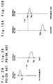
- step 120 If it is determined in the step 120 that the threshold voltage is equal to or lower than the voltage V EEV , whether the address counter AXY indicates a final memory cell address is determined in a step 124. If not the final memory cell address, the address counter AXY is incremented by "1" to execute the verifying operation to the next memory cell. If the final memory cell address, the over-erasing operation is completed. The distribution of threshold voltages after the over-erasure is shown in Fig. 10A.
- the programming-back operation is executed in units of memory blocks while a verifying operation is executed (step 102).
- an address counter AY and a counter DC are set to "0" in step 132 and 134.
- the programming-back operation is executed in a step 136.
- a high voltage is applied to the drains of memory cells and the sources are connected to the ground potential by the erasing circuit 5, column decoder 4 and programming circuit 7 in response to the control circuit 9 in this embodiment.
- the high voltage pulse having a relative long duration is repeatedly applied.
- the high voltage and the ground potential may be applied to the sources and the drains inversely.
- a high voltage may be supplied to the control gates of all the memory cell transistors by the row decoder 3 in response to the control circuit 9.
- a high voltage may be applied to the control gate.
- all the word line X0 to X n are selected and set in a high potential state by controlling the row decoder 3.
- the sources and drains may be set to a voltage close to about 0V.
- the counter DC is incremented by "1" in a step 138.
- a step 140 whether the threshold voltage is equal to or higher than a final target voltage, i.e., the threshold voltage lower limit V DV of about 0.5V is checked.
- the programming-back operation is repeated in the step 136.
- the memory device is determined to be defective.
- a verifying operation is executed in the step 140.
- the sense amplifier 6, the erasing circuit 5 and the row decoder 3 are controlled by the control circuit 9 such that the source is grounded, a predetermined voltage is applied to the control gate and the sense amplifier detects the data read out from the memory cells. If the verifying operation is passed in the step 140, whether the address counter AY indicates the final column address is checked in a step S144. If not, the address counter AY is incremented by "1", the verifying operation is executed to the next column in the step 140.
- a threshold voltage upper limit checking operation is executed in a step 103.
- an address counter AXY is set to "0" in a step 152.
- a verifying operation is executed to ensure that the threshold voltage of each memory cell is equal to or lower than a final target value of V EV .
- the verifying operation is executed in the same manner as described above by changing the reference voltage. If not in the step 154, the memory device is determined to be detective.
- the step 154 is passed, whether the address counter AXY indicates the final memory address is checked in a step 156. If not, a step 158 is executed to increment the address counter AXY by "1" and then the verifying operation is executed to the next memory cell. If yes in the step 156, the initializing operation is completed. At this time, the upper limit of the distribution of threshold voltages is ensured.
- the reason why the over-erasing operation is executed in the step 101 is the following notable matters.
- the erasing operation is difficult to be executed because of the memory cell characteristics when the threshold voltage has become negative so that an electric field becomes small. This means that the lower limit of the threshold voltages saturates with a negative value, so that the distribution of threshold voltages can be narrowed or converged.
- the over-erasure does not affect so much because of the verifying operation. If it is ensured that the distribution of threshold voltages is narrowed through the programming-back operation, the threshold voltage upper limit checking step 103 may be omitted. Further, if the distribution of threshold voltages is converged in the over-erasing operation, the verifying operation may be omitted from the step 101 so that only the over-erasing operation 101' is executed as shown in Fig. 11
- the initializing method in the second embodiment is the same as the initializing method of the first embodiment except that a pre-programming step which is the same as the pre-programming operation 201 in the conventional initializing method is added before the over-erasure routine 101 to the initializing method flow of the first embodiment. Therefore, the detail of pre-programming operation will not be described. Thereby, the distribution of threshold voltages can be further narrowed. The narrower the distribution of threshold voltages is before the erasing operation, the narrower the resultant distribution of threshold voltage after the initializing operation is. Further, since it is not necessary to execute the over-erasure to too much extent, a total erasing operation time is not increased.
- the present invention relates to an initializing method of an electrically erasable non-volatile semiconductor memory device such as a flash memory. Since the present invention employs a method in which the programming-back operation is executed to a memory block as well as a verifying operation until the memory cell threshold voltage lower limit becomes equal to or higher than a predetermined voltage, after the over-erasing operation is executed once, the distribution of threshold voltages can be narrowed to about 1/2 to 3/4 compared to the conventional initializing method as well as an abnormal operation caused by omitting the verifying operation and the increase of erasing operation time can be prevented.
- a method of initializing the electrically erasable non-volatile semiconductor memory device includes a step of repeating an over-erasing operation and verifying operation until an upper limit of the threshold voltages of the memory cells is equal to or lower than a predetermined voltage V EEV , a step of repeating the programming-back operation in which a high voltage is applied to the control gates of the memory cells or a high voltage is applied to one of the sources and drains of the memory cells while the other is connected to the ground potential, until a lower limit of the threshold voltages of the memory cells is equal to or higher than a second predetermined voltage (V DV ), a final routine of verifying that an upper limit of the threshold voltages of the memory is equal to or lower than a third predetermined voltage V EV , thereby the distribution of threshold voltages falls within a range equal to or higher than the second predetermined voltage V DV and equal to or lower than the third predetermined voltage V EV .
- the distribution of threshold voltages can be narrowed without damage to the reliability, and without increase of the erasing operation time and an abnormal operation caused by executing the erasing operation and the programming-back operation using a predetermined pulse with no verifying operation.
Landscapes
- Read Only Memory (AREA)
Applications Claiming Priority (2)
| Application Number | Priority Date | Filing Date | Title |
|---|---|---|---|
| JP236539/94 | 1994-09-30 | ||
| JP23653994A JPH08102198A (ja) | 1994-09-30 | 1994-09-30 | 電気的書換え可能な不揮発性半導体記憶装置の初期化方 法 |
Publications (2)
| Publication Number | Publication Date |
|---|---|
| EP0704853A2 true EP0704853A2 (de) | 1996-04-03 |
| EP0704853A3 EP0704853A3 (de) | 1998-08-19 |
Family
ID=17002177
Family Applications (1)
| Application Number | Title | Priority Date | Filing Date |
|---|---|---|---|
| EP95115474A Withdrawn EP0704853A3 (de) | 1994-09-30 | 1995-09-29 | Initialisierung einer elektrisch löschbaren nichtflüchtigen Halbleiterspeicheranordnung |
Country Status (3)
| Country | Link |
|---|---|
| US (1) | US5732019A (de) |
| EP (1) | EP0704853A3 (de) |
| JP (1) | JPH08102198A (de) |
Cited By (2)
| Publication number | Priority date | Publication date | Assignee | Title |
|---|---|---|---|---|
| EP0932161A1 (de) * | 1998-01-22 | 1999-07-28 | STMicroelectronics S.r.l. | Verfahren für kontrolliertes Löschen von Speicheranordnungen, insbesondere Analog- oder Mehrwert-Flash-EEPROM Anordnungen |
| EP0813209B1 (de) * | 1996-06-12 | 2004-10-20 | Texas Instruments Incorporated | Verfahren zum Löschen eines nichtflüchtigen Speichers |
Families Citing this family (16)
| Publication number | Priority date | Publication date | Assignee | Title |
|---|---|---|---|---|
| WO1997008707A1 (en) * | 1995-08-31 | 1997-03-06 | Hitachi, Ltd. | Semiconductor non-volatile memory device and computer system using the same |
| KR100323554B1 (ko) | 1997-05-14 | 2002-03-08 | 니시무로 타이죠 | 불휘발성반도체메모리장치 |
| JP2000276882A (ja) * | 1999-03-23 | 2000-10-06 | Nec Corp | 不揮発性半導体記憶装置とその記憶データの消去方法 |
| US6122198A (en) * | 1999-08-13 | 2000-09-19 | Advanced Micro Devices, Inc. | Bit by bit APDE verify for flash memory applications |
| JP4138173B2 (ja) | 1999-08-26 | 2008-08-20 | 株式会社ルネサステクノロジ | 不揮発性半導体記憶装置およびその消去方法 |
| US7061810B2 (en) * | 2001-10-09 | 2006-06-13 | Micron Technology, Inc. | Erasing flash memory without pre-programming the flash memory before erasing |
| KR100606173B1 (ko) * | 2004-08-24 | 2006-08-01 | 삼성전자주식회사 | 불휘발성 메모리 장치의 초기화 상태를 검증하는 방법 및장치 |
| US7079424B1 (en) * | 2004-09-22 | 2006-07-18 | Spansion L.L.C. | Methods and systems for reducing erase times in flash memory devices |
| US7230851B2 (en) * | 2004-12-23 | 2007-06-12 | Sandisk Corporation | Reducing floating gate to floating gate coupling effect |
| US7345918B2 (en) * | 2005-08-31 | 2008-03-18 | Micron Technology, Inc. | Selective threshold voltage verification and compaction |
| US7701780B2 (en) * | 2007-05-31 | 2010-04-20 | Micron Technology, Inc. | Non-volatile memory cell healing |
| US7986553B2 (en) * | 2007-06-15 | 2011-07-26 | Micron Technology, Inc. | Programming of a solid state memory utilizing analog communication of bit patterns |
| JP2011258260A (ja) | 2010-06-07 | 2011-12-22 | Toshiba Corp | 不揮発性半導体記憶装置 |
| US9589639B1 (en) | 2015-11-04 | 2017-03-07 | International Business Machines Corporation | Multiple FET non-volatile memory with default logical state |
| CN114283864A (zh) * | 2021-11-19 | 2022-04-05 | 成都博尔微晶科技有限公司 | 一种存储单元的擦除方法、装置、电子设备及存储介质 |
| US12249365B2 (en) * | 2023-03-06 | 2025-03-11 | Windbond Electronics Corp. | Memory device capable of performing in-memory computing |
Family Cites Families (10)
| Publication number | Priority date | Publication date | Assignee | Title |
|---|---|---|---|---|
| DE69013237T2 (de) * | 1989-06-19 | 1995-02-23 | Texas Instruments Inc | Schaltung und Verfahren zur Vorbereitung gelöschter EEPROMS vor der Programmierung. |
| JP2709751B2 (ja) * | 1990-06-15 | 1998-02-04 | 三菱電機株式会社 | 不揮発性半導体記憶装置およびそのデータ消去方法 |
| US5272669A (en) * | 1991-02-20 | 1993-12-21 | Sundisk Corporation | Method and structure for programming floating gate memory cells |
| JPH0574182A (ja) * | 1991-09-10 | 1993-03-26 | Nec Corp | 不揮発性半導体記憶装置 |
| JPH05182480A (ja) * | 1991-12-28 | 1993-07-23 | Sony Corp | プログラマブルリードオンリメモリ |
| JPH05235368A (ja) * | 1992-02-19 | 1993-09-10 | Nec Corp | データ消去方法 |
| JP3061924B2 (ja) * | 1992-03-02 | 2000-07-10 | 日本電気株式会社 | 不揮発性記憶装置の消去方法 |
| JPH0628875A (ja) * | 1992-07-10 | 1994-02-04 | Sony Corp | フラッシュ型e2 promの消去方法 |
| US5452251A (en) * | 1992-12-03 | 1995-09-19 | Fujitsu Limited | Semiconductor memory device for selecting and deselecting blocks of word lines |
| JPH07320488A (ja) * | 1994-05-19 | 1995-12-08 | Hitachi Ltd | 一括消去型不揮発性記憶装置とその消去方法 |
-
1994
- 1994-09-30 JP JP23653994A patent/JPH08102198A/ja active Pending
-
1995
- 1995-09-29 EP EP95115474A patent/EP0704853A3/de not_active Withdrawn
-
1997
- 1997-05-19 US US08/858,916 patent/US5732019A/en not_active Expired - Lifetime
Cited By (3)
| Publication number | Priority date | Publication date | Assignee | Title |
|---|---|---|---|---|
| EP0813209B1 (de) * | 1996-06-12 | 2004-10-20 | Texas Instruments Incorporated | Verfahren zum Löschen eines nichtflüchtigen Speichers |
| EP0932161A1 (de) * | 1998-01-22 | 1999-07-28 | STMicroelectronics S.r.l. | Verfahren für kontrolliertes Löschen von Speicheranordnungen, insbesondere Analog- oder Mehrwert-Flash-EEPROM Anordnungen |
| US6091642A (en) * | 1998-01-22 | 2000-07-18 | Stmicroelectronics, S.R.L. | Method for controlled erasing memory devices, in particular analog and multi-level flash-EEPROM devices |
Also Published As
| Publication number | Publication date |
|---|---|
| JPH08102198A (ja) | 1996-04-16 |
| US5732019A (en) | 1998-03-24 |
| EP0704853A3 (de) | 1998-08-19 |
Similar Documents
| Publication | Publication Date | Title |
|---|---|---|
| US7082060B2 (en) | Soft programming for recovery of overerasure | |
| US6777292B2 (en) | Set of three level concurrent word line bias conditions for a NOR type flash memory array | |
| US5732019A (en) | Initialization of electrically erasable non-volatile semiconductor memory device | |
| EP0857346B1 (de) | Überlöschungskorrektur für flash-speicher mit überlöschungsbegrenzung und vermeidung von löschprüffehlern | |
| KR0172441B1 (ko) | 불휘발성 반도체 메모리의 프로그램 방법 | |
| US6567316B1 (en) | Nonvolatile semiconductor memory device and method of erasing data of nonvolatile semiconductor memory device | |
| US6574147B2 (en) | Electrically erasable and programmable nonvolatile semiconductor memory with automatic write-verify controller | |
| US6577540B2 (en) | Flash memory device capable of preventing an over-erase of flash memory cells and erase method thereof | |
| US7072221B2 (en) | Flash memory device and method for driving the same | |
| US20090135656A1 (en) | Non-volatile semiconductor memory device with dummy cells and method of programming the same | |
| US6137729A (en) | Method for erasing memory cells in a flash memory device | |
| US6011722A (en) | Method for erasing and programming memory devices | |
| US6438037B1 (en) | Threshold voltage compacting for non-volatile semiconductor memory designs | |
| US5576991A (en) | Multistepped threshold convergence for a flash memory array | |
| US6542410B2 (en) | Nonvolatile semiconductor memory device capable of reducing pre-erase write time and erase method therefor | |
| US6657898B2 (en) | Nonvolatile semiconductor memory device and data erase method therefor | |
| KR20040044360A (ko) | 불휘발성반도체기억장치 및 그 데이터소거방법 | |
| US5784317A (en) | Flash memory device using an operational circuit for bit-by-bit verifying of programmed data in memory cells and method of programming the same | |
| US6914827B2 (en) | Flash memory device capable of preventing an over-erase of flash memory cells and erase method thereof | |
| US6240023B1 (en) | Method for efficiently executing soft programming of a memory block | |
| KR101405405B1 (ko) | 더미 셀들을 갖는 불휘발성 반도체 메모리 장치 및 더미셀들의 문턱전압 조절방법 | |
| CN100388391C (zh) | 或非闪速内存单元在高列泄漏下精确确认的装置与方法 | |
| JP2002025279A (ja) | 不揮発性半導体メモリ装置の消去方法 | |
| US5579261A (en) | Reduced column leakage during programming for a flash memory array | |
| US6373750B1 (en) | Non-volatile memory which performs erasure in a short time |
Legal Events
| Date | Code | Title | Description |
|---|---|---|---|
| PUAI | Public reference made under article 153(3) epc to a published international application that has entered the european phase |
Free format text: ORIGINAL CODE: 0009012 |
|
| AK | Designated contracting states |
Kind code of ref document: A2 Designated state(s): DE FR IT |
|
| PUAL | Search report despatched |
Free format text: ORIGINAL CODE: 0009013 |
|
| AK | Designated contracting states |
Kind code of ref document: A3 Designated state(s): DE FR IT |
|
| 17P | Request for examination filed |
Effective date: 19981130 |
|
| 17Q | First examination report despatched |
Effective date: 20000308 |
|
| STAA | Information on the status of an ep patent application or granted ep patent |
Free format text: STATUS: THE APPLICATION IS DEEMED TO BE WITHDRAWN |
|
| 18D | Application deemed to be withdrawn |
Effective date: 20010529 |