EP0704972B1 - Ausgangschaltung für eine Sende-/Empfangslogik vom Typ "gunning" - Google Patents
Ausgangschaltung für eine Sende-/Empfangslogik vom Typ "gunning" Download PDFInfo
- Publication number
- EP0704972B1 EP0704972B1 EP95115164A EP95115164A EP0704972B1 EP 0704972 B1 EP0704972 B1 EP 0704972B1 EP 95115164 A EP95115164 A EP 95115164A EP 95115164 A EP95115164 A EP 95115164A EP 0704972 B1 EP0704972 B1 EP 0704972B1
- Authority
- EP
- European Patent Office
- Prior art keywords
- coupled
- gate
- output
- transistor
- circuit
- Prior art date
- Legal status (The legal status is an assumption and is not a legal conclusion. Google has not performed a legal analysis and makes no representation as to the accuracy of the status listed.)
- Expired - Lifetime
Links
- 230000005669 field effect Effects 0.000 claims 12
- 239000004065 semiconductor Substances 0.000 description 9
- 230000005540 biological transmission Effects 0.000 description 7
- 230000001939 inductive effect Effects 0.000 description 7
- 238000010586 diagram Methods 0.000 description 6
- 230000000737 periodic effect Effects 0.000 description 4
- 230000003111 delayed effect Effects 0.000 description 2
- 230000003071 parasitic effect Effects 0.000 description 2
- 238000010276 construction Methods 0.000 description 1
- 230000000452 restraining effect Effects 0.000 description 1
- 230000008054 signal transmission Effects 0.000 description 1
Images


Classifications
-
- H—ELECTRICITY
- H03—ELECTRONIC CIRCUITRY
- H03K—PULSE TECHNIQUE
- H03K19/00—Logic circuits, i.e. having at least two inputs acting on one output; Inverting circuits
-
- H—ELECTRICITY
- H03—ELECTRONIC CIRCUITRY
- H03K—PULSE TECHNIQUE
- H03K19/00—Logic circuits, i.e. having at least two inputs acting on one output; Inverting circuits
- H03K19/003—Modifications for increasing the reliability for protection
- H03K19/00346—Modifications for eliminating interference or parasitic voltages or currents
- H03K19/00361—Modifications for eliminating interference or parasitic voltages or currents in field effect transistor circuits
-
- H—ELECTRICITY
- H03—ELECTRONIC CIRCUITRY
- H03K—PULSE TECHNIQUE
- H03K19/00—Logic circuits, i.e. having at least two inputs acting on one output; Inverting circuits
- H03K19/0175—Coupling arrangements; Interface arrangements
- H03K19/0185—Coupling arrangements; Interface arrangements using field effect transistors only
- H03K19/018557—Coupling arrangements; Impedance matching circuits
- H03K19/018571—Coupling arrangements; Impedance matching circuits of complementary type, e.g. CMOS
Definitions
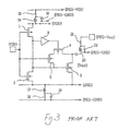
- the value of the potential is determined by a current flowing from the output terminal OUT to the earth line GND through the NMOS transistors 4, 5, and 2 and by ON resistances of the NMOS transistors 4, 5 and 2.
- the NMOS transistor 3 is allowed to be slightly turned ON state for the predetermined period of time determined by the delay circuit 8, so that the ringing can be restrained.
- An object of the present invention is to provide an output circuit capable of restraining sufficiently occurrence of a ringing.
Landscapes
- Engineering & Computer Science (AREA)
- Computer Hardware Design (AREA)
- Physics & Mathematics (AREA)
- Computing Systems (AREA)
- General Engineering & Computer Science (AREA)
- Mathematical Physics (AREA)
- Logic Circuits (AREA)
- Electronic Switches (AREA)
- Networks Using Active Elements (AREA)
Claims (3)
- Ausgangsschaltung mit einem Eingangsanschluß (VIN), dem ein Datensignal zugeführt wird, einem ersten Transistor (2) eines ersten Leitfähigkeitstyps mit einem Gate, das mit dem Eingangsanschluß (VIN) verbunden ist, einem zweiten Transistor (1) eines zweiten Leitfähigkeitstyps mit einem Gate, das mit dem Eingangsanschluß (VIN) verbunden ist, wobei der erste und der zweite Transistor (1, 2) in Reihe zwischen eine erste und eine zweite Versorgungsleitung (VDD, GND) geschaltet sind, einem dritten Transistor (3) des ersten Leitfähigkeitstyps mit einem Gate, das mit einem Verbindungsknoten des ersten und des zweiten Transistors (1, 2) verbunden ist, wobei der dritte Transistor (3) zwischen einen Ausgangsanschluß (VOUT) und die zweite Versorgungsleitung (GND) geschaltet ist, einem vierten und einem fünften Transistor (4, 5) mit jeweils dem ersten Leitfähigkeitstyp, die in Reihe zwischen den Ausgangsanschluß (VOUT) und das Gate des dritten Feldeffekttransistors (5) geschaltet sind, wobei der fünfte Feldeffekttransistor (5) ein Gate aufweist, das mit dem Eingabeanschluß (VIN) verbunden ist, und einer ersten Verzögerungsschaltung (8), die zwischen den Verbindungsknoten und das Gate des vierten Feldeffekttransistors (4) geschaltet ist,
gekennzeichnet durch weiterhin eine Ausgangsimpedanz-Steuerschaltung, die mit dem Ausgangsanschluß (VOUT) verbunden ist und die Impedanz am Ausgangsanschluß (VOUT) steuert, wenn sich das Datensignal ändert, wobei die Ausgangsimpedanz-Steuerschaltung (13) einen sechsten und einen siebenten Transistor (6, 7) mit jeweils dem ersten Leitfähigkeitstyp aufweist, die in Reihe zwischen den Ausgangsanschluß (VOUT) und das Gate des dritten Feldeffekttransistors (3) geschaltet sind, und eine zweite Verzögerungsschaltung (9), die zwischen die erste Verzögerungsschaltung (8) und das Gate des sechsten Transistors (6) geschaltet ist, wobei der siebente Transistor (7) ein Gate aufweist, das mit dem Eingangsanschluß (VIN) verbunden ist. - Ausgangsschaltung mit einem Eingabeanschluß (VIN), dem ein Datensignal zugeführt wird, einem ersten Transistor (2) eines ersten Leitfähigkeitstyps mit einem Gate, das mit dem Eingangsanschluß (VIN) verbunden ist, einem zweiten Transistor (1) eines zweiten Leitfähigkeitstyps mit einem Gate, das mit dem Eingangsanschluß (VIN) verbunden ist, wobei der erste und der zweite Transistor (1, 2) in Reihe zwischen eine erste und eine zweite Versorgungsleitung (VDD, GND) geschaltet sind, einem dritten Transistor (3) des ersten Leitfähigkeitstyps mit einem Gate, das mit einem Verbindungsknoten des ersten und des zweiten Transistors (1, 2) verbunden ist, wobei der dritte Transistor (3) zwischen einen Ausgangsanschluß (VOUT) und die zweite Versorgungsleitung (GND) geschaltet ist, einem vierten und einem fünften Transistor (4, 5) mit jeweils dem ersten Leitfähigkeitstyp, die in Reihe zwischen den Ausgangsanschluß (VOUT) und das Gate des dritten Feldeffekttransistors (5) geschaltet sind, wobei der fünfte Feldeffekttransistor (5) ein Gate aufweist, das mit dem Eingangsanschluß (VIN) verbunden ist und einer ersten Verzögerungsschaltung (8), die zwischen den Verbindungsknoten und das Gate des vierten Feldeffekttransistors (4) geschaltet ist,
gekennzeichnet durch weiterhin eine Ausgangsimpedanz-Steuerschaltung, die mit dem Ausgangsanschluß (VOUT) verbunden ist und die Impedanz an dem Ausgangsanschluß (VOUT) steuert, wenn sich das Datensignal ändert, wobei die Ausgangsimpedanz-Steuerschaltung (6-13) einen achten Feldeffekttransistor (10) des ersten Leitfähigkeitstyps aufweist, der zwischen den Ausgabeanschluß (VOUT) und die zweite Versorgungsleitung (GND) geschaltet ist, einen neunten und einen zehnten Transistor (6, 7), die in Reihe zwischen den Ausgangsanschluß (VOUT) und das Gate des achten Feldeffekttransistors (10) geschaltet sind, eine zweite und eine dritte Verzögerungsschaltung (11, 12), die in Reihe zwischen die erste Verzögerungsschaltung (8) und das Gate des neunten Feldeffekttransistors (6) geschaltet sind, und eine Logikschaltung mit einem ersten Eingangsknoten, der mit dem Eingangsanschluß (VIN) verbunden ist, einem zweiten Eingangsknoten, der mit einem Ausgangsanschluß der zweiten Verzögerungsschaltung (11) verbunden ist, und einem Ausgangsknoten, der mit dem Gate des achten Feldeffekttransistors (10) verbunden ist, wobei der zehnte Feldeffekttransistor (7) ein Gate aufweist, das mit dem Eingangsanschluß (VIN) verbunden ist. - Ausgangsschaltung nach Anspruch 2,
dadurch gekennzeichnet, daß die Logikschaltung (13) ein NAND-Gatter ist.
Applications Claiming Priority (2)
| Application Number | Priority Date | Filing Date | Title |
|---|---|---|---|
| JP6231257A JP2748865B2 (ja) | 1994-09-27 | 1994-09-27 | 出力回路 |
| JP231257/94 | 1994-09-27 |
Publications (3)
| Publication Number | Publication Date |
|---|---|
| EP0704972A2 EP0704972A2 (de) | 1996-04-03 |
| EP0704972A3 EP0704972A3 (de) | 1996-09-18 |
| EP0704972B1 true EP0704972B1 (de) | 1998-08-26 |
Family
ID=16920787
Family Applications (1)
| Application Number | Title | Priority Date | Filing Date |
|---|---|---|---|
| EP95115164A Expired - Lifetime EP0704972B1 (de) | 1994-09-27 | 1995-09-26 | Ausgangschaltung für eine Sende-/Empfangslogik vom Typ "gunning" |
Country Status (5)
| Country | Link |
|---|---|
| US (1) | US5563542A (de) |
| EP (1) | EP0704972B1 (de) |
| JP (1) | JP2748865B2 (de) |
| KR (1) | KR100191880B1 (de) |
| DE (1) | DE69504265T2 (de) |
Families Citing this family (9)
| Publication number | Priority date | Publication date | Assignee | Title |
|---|---|---|---|---|
| JP2783183B2 (ja) * | 1995-03-09 | 1998-08-06 | 日本電気株式会社 | 出力回路 |
| US5898688A (en) * | 1996-05-24 | 1999-04-27 | Cisco Technology, Inc. | ATM switch with integrated system bus |
| JPH10200051A (ja) * | 1997-01-14 | 1998-07-31 | Canon Inc | 半導体集積回路 |
| US6670822B2 (en) | 1998-08-11 | 2003-12-30 | Fairchild Semiconductor Corporation | Transceiver driver with programmable edge rate control independent of fabrication process, supply voltage, and temperature |
| US6184717B1 (en) | 1998-12-09 | 2001-02-06 | Nortel Networks Limited | Digital signal transmitter and receiver using source based reference logic levels |
| US6218863B1 (en) | 1999-04-12 | 2001-04-17 | Intel Corporation | Dual mode input/output interface circuit |
| JP2005086662A (ja) * | 2003-09-10 | 2005-03-31 | Seiko Epson Corp | 半導体装置 |
| CN110545047B (zh) * | 2019-10-17 | 2024-07-30 | 无锡麟力科技有限公司 | 小功率片内整流桥电路 |
| JP7709075B2 (ja) * | 2021-08-25 | 2025-07-16 | 株式会社ソシオネクスト | 半導体集積回路装置 |
Family Cites Families (8)
| Publication number | Priority date | Publication date | Assignee | Title |
|---|---|---|---|---|
| JPH0323715A (ja) * | 1989-06-20 | 1991-01-31 | Mitsubishi Electric Corp | 出力回路 |
| JPH0323712A (ja) * | 1989-06-20 | 1991-01-31 | Mitsubishi Electric Corp | 半導体集積回路 |
| JPH03232193A (ja) * | 1990-02-06 | 1991-10-16 | Mitsubishi Electric Corp | 出力回路 |
| US5023488A (en) * | 1990-03-30 | 1991-06-11 | Xerox Corporation | Drivers and receivers for interfacing VLSI CMOS circuits to transmission lines |
| US5148056A (en) * | 1991-03-27 | 1992-09-15 | Mos Electronics Corp. | Output buffer circuit |
| US5408146A (en) * | 1992-01-31 | 1995-04-18 | Lsi Logic Corporation | High performance backplane driver circuit |
| JP2894897B2 (ja) * | 1992-07-06 | 1999-05-24 | 富士通株式会社 | 半導体集積回路 |
| US5347169A (en) * | 1992-09-08 | 1994-09-13 | Preslar Donald R | Inductive load dump circuit |
-
1994
- 1994-09-27 JP JP6231257A patent/JP2748865B2/ja not_active Expired - Fee Related
-
1995
- 1995-09-22 US US08/532,986 patent/US5563542A/en not_active Expired - Lifetime
- 1995-09-26 EP EP95115164A patent/EP0704972B1/de not_active Expired - Lifetime
- 1995-09-26 DE DE69504265T patent/DE69504265T2/de not_active Expired - Lifetime
- 1995-09-27 KR KR1019950033794A patent/KR100191880B1/ko not_active Expired - Fee Related
Also Published As
| Publication number | Publication date |
|---|---|
| EP0704972A3 (de) | 1996-09-18 |
| KR100191880B1 (ko) | 1999-06-15 |
| DE69504265T2 (de) | 1999-04-22 |
| JP2748865B2 (ja) | 1998-05-13 |
| EP0704972A2 (de) | 1996-04-03 |
| JPH0897676A (ja) | 1996-04-12 |
| KR960012723A (ko) | 1996-04-20 |
| DE69504265D1 (de) | 1998-10-01 |
| US5563542A (en) | 1996-10-08 |
Similar Documents
| Publication | Publication Date | Title |
|---|---|---|
| US6593795B2 (en) | Level adjustment circuit and data output circuit thereof | |
| US5166555A (en) | Drive circuit comprising a subsidiary drive circuit | |
| US5041741A (en) | Transient immune input buffer | |
| KR950009087B1 (ko) | 반도체 집적회로의 출력회로 | |
| US6094086A (en) | High drive CMOS output buffer with fast and slow speed controls | |
| US5192879A (en) | MOS transistor output circuit | |
| KR960011964B1 (ko) | 출력버퍼장치 | |
| US4782252A (en) | Output current control circuit for reducing ground bounce noise | |
| US5313118A (en) | High-speed, low-noise, CMOS output driver | |
| US5148056A (en) | Output buffer circuit | |
| US5563542A (en) | Output circuit for gunning transceiver logic | |
| US4963774A (en) | Intermediate potential setting circuit | |
| KR100373432B1 (ko) | Gtl출력증폭기 | |
| EP1341307B1 (de) | Gegen Temperatur-, Spannungs- und Herstellungsschwankungen kompensierte Logikschaltung | |
| KR100300687B1 (ko) | 반도체집적회로 | |
| US5995440A (en) | Off-chip driver and receiver circuits for multiple voltage level DRAMs | |
| EP1292031A2 (de) | Integrierte Schaltung und Verfahren zur Einstellung der Kapazität eines Knotens in einer integrierten Schaltung | |
| KR100298444B1 (ko) | 입력 버퍼 회로 | |
| US20020180495A1 (en) | CMOS output circuit | |
| US6236235B1 (en) | Output circuit | |
| EP0821484B1 (de) | Hohen Spannungen widerstehende Ausgangsstufe | |
| KR100604809B1 (ko) | 듀티보상회로를 구비하는 출력드라이버 | |
| KR100205094B1 (ko) | 반도체 소자의 출력버퍼 회로 | |
| JP3125764B2 (ja) | 論理回路 | |
| JP2618884B2 (ja) | 半導体出力回路 |
Legal Events
| Date | Code | Title | Description |
|---|---|---|---|
| PUAI | Public reference made under article 153(3) epc to a published international application that has entered the european phase |
Free format text: ORIGINAL CODE: 0009012 |
|
| AK | Designated contracting states |
Kind code of ref document: A2 Designated state(s): DE FR GB |
|
| PUAL | Search report despatched |
Free format text: ORIGINAL CODE: 0009013 |
|
| AK | Designated contracting states |
Kind code of ref document: A3 Designated state(s): DE FR GB |
|
| 17P | Request for examination filed |
Effective date: 19960805 |
|
| 17Q | First examination report despatched |
Effective date: 19970326 |
|
| GRAG | Despatch of communication of intention to grant |
Free format text: ORIGINAL CODE: EPIDOS AGRA |
|
| GRAG | Despatch of communication of intention to grant |
Free format text: ORIGINAL CODE: EPIDOS AGRA |
|
| GRAH | Despatch of communication of intention to grant a patent |
Free format text: ORIGINAL CODE: EPIDOS IGRA |
|
| GRAH | Despatch of communication of intention to grant a patent |
Free format text: ORIGINAL CODE: EPIDOS IGRA |
|
| GRAA | (expected) grant |
Free format text: ORIGINAL CODE: 0009210 |
|
| AK | Designated contracting states |
Kind code of ref document: B1 Designated state(s): DE FR GB |
|
| REF | Corresponds to: |
Ref document number: 69504265 Country of ref document: DE Date of ref document: 19981001 |
|
| ET | Fr: translation filed | ||
| PLBE | No opposition filed within time limit |
Free format text: ORIGINAL CODE: 0009261 |
|
| STAA | Information on the status of an ep patent application or granted ep patent |
Free format text: STATUS: NO OPPOSITION FILED WITHIN TIME LIMIT |
|
| 26N | No opposition filed | ||
| REG | Reference to a national code |
Ref country code: GB Ref legal event code: IF02 |
|
| REG | Reference to a national code |
Ref country code: GB Ref legal event code: 732E |
|
| REG | Reference to a national code |
Ref country code: FR Ref legal event code: TP |
|
| REG | Reference to a national code |
Ref country code: FR Ref legal event code: CD |
|
| REG | Reference to a national code |
Ref country code: DE Ref legal event code: R082 Ref document number: 69504265 Country of ref document: DE Representative=s name: GLAWE DELFS MOLL - PARTNERSCHAFT VON PATENT- U, DE |
|
| REG | Reference to a national code |
Ref country code: DE Ref legal event code: R082 Ref document number: 69504265 Country of ref document: DE Representative=s name: GLAWE DELFS MOLL PARTNERSCHAFT MBB VON PATENT-, DE Effective date: 20120828 Ref country code: DE Ref legal event code: R082 Ref document number: 69504265 Country of ref document: DE Representative=s name: GLAWE DELFS MOLL - PARTNERSCHAFT VON PATENT- U, DE Effective date: 20120828 Ref country code: DE Ref legal event code: R081 Ref document number: 69504265 Country of ref document: DE Owner name: RENESAS ELECTRONICS CORPORATION, KAWASAKI-SHI, JP Free format text: FORMER OWNER: NEC ELECTRONICS CORP., KAWASAKI, KANAGAWA, JP Effective date: 20120828 Ref country code: DE Ref legal event code: R081 Ref document number: 69504265 Country of ref document: DE Owner name: RENESAS ELECTRONICS CORPORATION, JP Free format text: FORMER OWNER: NEC ELECTRONICS CORP., KAWASAKI, JP Effective date: 20120828 |
|
| PGFP | Annual fee paid to national office [announced via postgrant information from national office to epo] |
Ref country code: DE Payment date: 20130918 Year of fee payment: 19 |
|
| PGFP | Annual fee paid to national office [announced via postgrant information from national office to epo] |
Ref country code: FR Payment date: 20130910 Year of fee payment: 19 Ref country code: GB Payment date: 20130925 Year of fee payment: 19 |
|
| REG | Reference to a national code |
Ref country code: DE Ref legal event code: R119 Ref document number: 69504265 Country of ref document: DE |
|
| GBPC | Gb: european patent ceased through non-payment of renewal fee |
Effective date: 20140926 |
|
| REG | Reference to a national code |
Ref country code: DE Ref legal event code: R119 Ref document number: 69504265 Country of ref document: DE Effective date: 20150401 |
|
| REG | Reference to a national code |
Ref country code: FR Ref legal event code: ST Effective date: 20150529 |
|
| PG25 | Lapsed in a contracting state [announced via postgrant information from national office to epo] |
Ref country code: GB Free format text: LAPSE BECAUSE OF NON-PAYMENT OF DUE FEES Effective date: 20140926 Ref country code: DE Free format text: LAPSE BECAUSE OF NON-PAYMENT OF DUE FEES Effective date: 20150401 |
|
| PG25 | Lapsed in a contracting state [announced via postgrant information from national office to epo] |
Ref country code: FR Free format text: LAPSE BECAUSE OF NON-PAYMENT OF DUE FEES Effective date: 20140930 |