EP0705026A1 - Appareil et procédé pour le codage et la reconstruction de données d'image - Google Patents
Appareil et procédé pour le codage et la reconstruction de données d'image Download PDFInfo
- Publication number
- EP0705026A1 EP0705026A1 EP95306903A EP95306903A EP0705026A1 EP 0705026 A1 EP0705026 A1 EP 0705026A1 EP 95306903 A EP95306903 A EP 95306903A EP 95306903 A EP95306903 A EP 95306903A EP 0705026 A1 EP0705026 A1 EP 0705026A1
- Authority
- EP
- European Patent Office
- Prior art keywords
- pixel
- bit
- image
- bit stream
- state
- Prior art date
- Legal status (The legal status is an assumption and is not a legal conclusion. Google has not performed a legal analysis and makes no representation as to the accuracy of the status listed.)
- Granted
Links
- 238000000034 method Methods 0.000 title claims description 36
- 238000012545 processing Methods 0.000 claims abstract description 20
- 239000000758 substrate Substances 0.000 claims 1
- 238000012546 transfer Methods 0.000 description 41
- 238000013459 approach Methods 0.000 description 8
- 238000010586 diagram Methods 0.000 description 6
- 101100191136 Arabidopsis thaliana PCMP-A2 gene Proteins 0.000 description 5
- 101100048260 Saccharomyces cerevisiae (strain ATCC 204508 / S288c) UBX2 gene Proteins 0.000 description 5
- 230000003044 adaptive effect Effects 0.000 description 5
- 230000006835 compression Effects 0.000 description 5
- 238000007906 compression Methods 0.000 description 5
- 230000006837 decompression Effects 0.000 description 4
- 230000000694 effects Effects 0.000 description 4
- 230000006870 function Effects 0.000 description 4
- 230000015556 catabolic process Effects 0.000 description 3
- 238000006731 degradation reaction Methods 0.000 description 3
- 230000003139 buffering effect Effects 0.000 description 2
- 238000009432 framing Methods 0.000 description 2
- 238000003384 imaging method Methods 0.000 description 2
- 230000004913 activation Effects 0.000 description 1
- 230000005540 biological transmission Effects 0.000 description 1
- 238000006243 chemical reaction Methods 0.000 description 1
- 238000004891 communication Methods 0.000 description 1
- 238000012937 correction Methods 0.000 description 1
- 238000011161 development Methods 0.000 description 1
- 230000009191 jumping Effects 0.000 description 1
- 238000012544 monitoring process Methods 0.000 description 1
- 108091008695 photoreceptors Proteins 0.000 description 1
- 238000012216 screening Methods 0.000 description 1
- 230000001360 synchronised effect Effects 0.000 description 1
- 238000013519 translation Methods 0.000 description 1
Images



Classifications
-
- H—ELECTRICITY
- H04—ELECTRIC COMMUNICATION TECHNIQUE
- H04N—PICTORIAL COMMUNICATION, e.g. TELEVISION
- H04N1/00—Scanning, transmission or reproduction of documents or the like, e.g. facsimile transmission; Details thereof
- H04N1/41—Bandwidth or redundancy reduction
- H04N1/411—Bandwidth or redundancy reduction for the transmission or storage or reproduction of two-tone pictures, e.g. black and white pictures
Definitions
- the present invention relates generally to a technique for both storing and outputting image data in a printing system and, more particularly, to an apparatus and method in which image data, from an input image, is encoded and the resulting encoded bitstream is then reconstructed.
- Electronic printing systems typically include an input section, sometimes referred to as an input image terminal ("IIT”), a controller, sometimes referred to as an electronic subsystem ("ESS”) and an output section or print engine, sometimes referred to as an image output terminal ("IOT").
- IIT input image terminal
- ESS electronic subsystem
- IOT image output terminal
- a job can be inputted to the IIT from, among other sources, a network or a scanner.
- An example of an IIT with both network and scanner inputs is found in US-A-5,170,340.
- output of an image can be enhanced significantly through use of a high addressability output device.
- a printing machine with a capability of storing or buffering scanned data prepared at a resolution of 600 x 3 spi, a corresponding output of 1800 x 1 spi can be obtained. While this sort of output is desirable, storing image data at 600 x 3 spi, even for short time periods, can be burdensome on a printing machine with relatively limited volatile or system memory, such as some of the digital printing systems discussed above. While various ones of the above printing systems advantageously exploit disk storage, in conjunction with system memory, it is, for purposes of outputting a job, necessary to store or buffer the job in system memory.
- storing or buffering a job at less than 600 x 3 spi is accomplished by discarding image-related information, i.e. image data.
- image data can lead to a degradation of image quality when reproducing the remaining image data. It would be desirable to provide a technique in which at least a part of the discarded image data could be reconstructed so that image degradation is minimized.
- an apparatus for processing an input image represented by image data the image data assuming a form of an input bit stream, the input bit stream including a plurality of first bit sets
- the invention thus provides an apparatus and method in which image data, from an input image, is discarded, during an encoding process, and a resulting encoded bitstream is reconstructed in a manner which serves to replenish a substantial amount of the discarded image data and minimize degradation of an output representation of the input image.
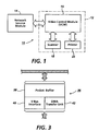
- the printing system 10 includes a printing machine 12 operatively coupled with a network service module 14.
- the printing machine 12 includes an electronic subsystem 16, referred to as a video control module (VCM), communicating with a scanner 18 and a printer 20.
- VCM video control module
- the VCM 16 which will be described in further detail below, coordinates the operation of the scanner and printer in a digital copying arrangement.
- the scanner 18 also referred to as image input terminal (IIT)
- IIT image input terminal
- an image processing system 22 ( Figure 2), associated with the scanner 18, executes signal correction and the like, converts the corrected signals into multi-level signals (e.g. binary signals), compresses the multi-level signals and preferably stores the same in electronic precollation (EPC) memory 24.
- EPC electronic precollation
- the printer 20 (also referred to as image output terminal (IOT)) preferably includes a xerographic print engine.
- the print engine has a multi-pitch belt (not shown) which is written on with an imaging source, such as a synchronous source (e.g. laser raster output scanning device) or an asynchronous source (e.g. LED print bar).
- an imaging source such as a synchronous source (e.g. laser raster output scanning device) or an asynchronous source (e.g. LED print bar).
- the multi-level image data is read out of the EPC memory 24 ( Figure 2) while the imaging source is turned on and off, in accordance with the image data, forming a latent image on the photoreceptor.
- the latent image is developed with, for example, a hybrid jumping development technique and transferred to a print media sheet.
- the printer can assume other forms besides a xerographic print engine without altering the concept upon which the disclosed embodiment is based.
- the printing system 10 could be implemented with a thermal ink jet or ionographic printer.
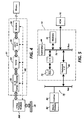
- the VCM 16 includes a video bus (VBus) 28 with which various I/O, data transfer and storage components communicate.
- VBus is a high speed, 32 bit data burst transfer bus which is expandable to 64 bit.
- the 32 bit implementation has a sustainable maximum bandwidth of approximately 60 MBytes/sec. In one example, the bandwidth of the VBus is as high as 100 MBytes/sec.
- the storage components of the VCM reside in the EPC memory section 30 and the mass memory section 32.
- the EPC memory section includes the EPC memory 24, the EPC memory being coupled with the VBus by way of a DRAM controller 33.
- the EPC memory which is preferably DRAM, provides expansion of up to 64 MBytes, by way of two high density 32 bit SIMM modules.
- the mass memory section 32 includes a SCSI hard drive device 34 coupled to the VBus by way of a transfer module 36a.
- transfer module 36a As will appear, other I/O and processing components are coupled respectively to the VBus by way of transfer modules 36. It will be appreciated that other devices (e.g. a workstation) could be coupled to the VBus by way of the transfer module 36a through use of a suitable interface and a SCSI line.
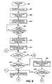
- the illustrated transfer module of Figure 3 includes a packet buffer 38, a VBus interface 40 and DMA transfer unit 42 .
- the transfer module 36 which was designed with "VHSIC" Hardware Description Language (VHDL), is a programmable arrangement permitting packets of image data to be transmitted along the VBus at a relatively high transfer rate.
- the packet buffer is programmable so that the segment or packet can be varied according to the available bandwidth of the VBus.
- the packet buffer can programmed to handle packets of up to 64 Bytes Preferably, the packet size would be reduced for times when the VBus is relatively busy and increased for times when activity on the bus is relatively low.
- Adjustment of the packet size is achieved with the VBus interface 40 and a system controller 44 ( Figure 5).
- the VBus interface is an arrangement of logical components, including, among others, address counters, decoders and state machines, which provides the transfer module with a selected degree of intelligence.
- the interface 40 communicates with the system controller to keep track of desired packet size and, in turn, this knowledge is used to adjust the packet size of the packet buffer 38, in accordance with bus conditions. That is, the controller, in view of its knowledge regarding conditions on the VBus 28, passes directives to the interface 40 so that the interface can adjust packet size accordingly. Further discussion regarding operation of the transfer module 36 is provided below
- each DMA transfer unit employs a conventional DMA transfer strategy to transfer the packets.
- the beginning and end addresses of the packet are used by the transfer unit in implementing a given transfer.
- the interface 40 transmits a signal back to the system controller 44 so that further information, such as desired packet size and address designations, can be obtained.
- FIG. 1 and 2 three I/O components are shown as being coupled operatively to the VBus 28, namely a FAX module 48, the scanner or IIT 18, and the printer or IOT 20; however, it should be recognized that a wide variety of components could be coupled to the VBus by way an expansion slot 50.
- a FAX module 48 which is coupled to the VBus 28 by way of transfer module 36b, is discussed in further detail.
- a facsimile device (FAX) 51 includes a chain of components, namely a section 52 for performing Xerox adaptive compression/decompression, a section 54 for scaling compressed image data, a section 56 for converting compressed image data to or from CCITT format, and a modem 58, preferably manufactured by Rockwell Corporation, for transmitting CCITT formatted data from or to a telephone, by way of a conventional communication line.
- a facsimile device (FAX) 51 includes a chain of components, namely a section 52 for performing Xerox adaptive compression/decompression, a section 54 for scaling compressed image data, a section 56 for converting compressed image data to or from CCITT format, and a modem 58, preferably manufactured by Rockwell Corporation, for transmitting CCITT formatted data from or to a telephone, by way of a conventional communication line.
- each of the sections 52, 54 and 56 as well as modem 58 are coupled with the transfer module 36b by way of a control line 60.
- This permits transfers to be made to and from the FAX module 48 without involving a processor.
- the transfer module 36b can serve as a master or slave for the FAX module in that the transfer module can provide image data to the FAX for purposes of transmission or receive an incoming FAX. In operation, the transfer module 36b reacts to the FAX module in the same manner that it would react to any other I/O component.
- the transfer module 36b feeds packets to the section 52 through use of the DMA transfer unit 42 and, once a packet is fed, the transfer module transmits an interrupt signal to the system processor 44 requesting another packet.
- the transfer module 36b two packets are maintained in the packet buffer 38 so that "ping-ponging" can occur between the two packets. In this way, the transfer module 36b does not run out of image data even when the controller cannot get back to it immediately upon receiving an interrupt signal.
- the IIT 18 and IOT 20 are operatively coupled to the VBus 28 by way of transfer modules 36c and 36d. Additionally, the IIT 18 and the IOT 20 are operatively coupled with a compressor 62 and a decompressor 64, respectively.
- the compressor and decompressor are preferably provided by way of a single module that employs Xerox adaptive compression devices. Xerox adaptive compression devices have been used for compression/decompression operations by Xerox Corporation in its DocuTech ® printing system. In practice, at least some of the functionality of the transfer modules is provided by way of a 3 channel DVMA device, which device provides local arbitration for the compression/decompression module.
- the scanner 18, which includes the image processing section 22, is coupled with an annotate/merge module 66.
- the image processing section includes one or more dedicated processors programmed to perform various desired functions, such as image enhancement, thresholding/screening, rotation, resolution conversion and TRC adjustment.
- the selective activation of each of these functions can be coordinated by a group of image processing control registers, the registers being programmed by the system controller 44.
- the functions are arranged along a "pipeline" in which image data is inputted to one end of the pipe, and image processed image data is outputted at the other end of the pipe.
- transfer module 36e is positioned at one end of the image processing section 22 and transfer module 36c is positioned at another end of the section 22. As will appear, positioning of transfer modules 36c and 36e in this manner greatly facilitates the concurrency of a loopback process.
- arbitration of the various bus masters of the VCM 16 is implemented by way of a VBus arbiter 70 disposed in a VBus arbiter/bus gateway 71.
- the arbiter determines which bus master (e.g. FAX module, Scanner, Printer, SCSI Hard Drive, EPC Memory or Network Service Component) can access the VBus at one given time.
- the arbiter is made up of two main sections and a third control section. The first section, i.e., the "Hi-Pass" section, receives input bus requests and current priority selection, and outputs a grant corresponding to the highest priority request pending.
- the current priority selection input is the output from the second section of the arbiter and is referred to as "Priority Select".
- This section implements priority rotation and selection algorithm.
- the output of the logic for priority select determines the order in which pending requests will be serviced.
- the input to Priority Select is a register which holds an initial placement of devices on a priority chain. On servicing requests, this logic moves the devices up and down the priority chain thereby selecting the position of a device's next request.
- Control logic synchronizes the tasks of the Hi-Pass and the Priority Select by monitoring signals regarding request/grant activity. It also prevents the possibility of race conditions.
- the network service module 14 is discussed in further detail.
- the architecture of the network service module is similar to that of a known "PC clone". More particularly, in the preferred embodiment, the controller 44, which preferably assumes the form of a SPARC processor, manufactured by Sun Microsystems, Inc., is coupled with a standard SBus 72.
- a host memory 74 which preferably assumes the form of DRAM, and a SCSI disk drive device 76 are coupled operatively to the SBus 72.
- a storage or I/O device could be coupled with the SBus with a suitable interface chip.
- the SBus is coupled with a network 78 by way of an appropriate network interface 80.
- the network interface includes all of the hardware and software necessary to relate the hardware/software components of the controller 44 with the hardware/software components of the network 78.
- the network interface could be provided with, among other software, Netware ® from Novell Corp.
- the network 78 includes a client, such as a workstation 82 with an emitter or driver 84.
- a user may generate a job including a plurality of electronic pages and a set of processing instructions.
- the job is converted, with the emitter, into a representation written in a page description language, such as PostScript.
- the job is then transmitted to the controller 44 where it is interpreted with a decomposer, such as one provided by Adobe Corporation.
- the network service module 14 is coupled with the VCM 16 via a bus gateway 88 of the VBus arbiter/bus gateway 71.
- the bus gateway comprises a field programmable gate array provided by XILINX corporation.
- the bus gateway device provides the interface between the host SBus and the VCM VBus. It provides VBus address translation for accesses to address spaces in the VBus real address range, and passes a virtual address to the host SBus for virtual addresses in the host address range.
- a DMA channel for memory to memory transfers is also implemented in the bus gateway.
- the bus gateway provides seamless access between the VBus and SBus, and decodes virtual addresses from bus masters, such as one of the transfer modules 36, so that an identifier can be obtained from a corresponding slave component. It will be appreciated by those skilled in the art that many components of the printing system 10 are implemented in the form of a single ASIC.
- each of the transfer modules 36 comprises a plurality of packets.
- one of the transfer modules 36 is provided, by the controller 44, with the beginning address of a block and the size of the block.
- the transfer module 36 effects a packet tranfer and increments/decrements a counter. This procedure is repeated for each packet of the block until the interface 40 determines, by reference to the counter, that the last packet of the block has been transferred.
- several blocks are transferred, in a packet-by-packet manner, as described immediately above.
- input image data for a given input image
- image processing section 22 Figure 2
- the inputted image data is obtained at the scanner 18. More particularly, a document is scanned and 2 X bits of gray data is provided in the form of a bitstream.
- the gray data is thresholded so that the image is expressed as n bits of data where n is less than 2 X .
- image data is encoded.
- n bits are described with n - m bits where each m bit represents, as explained in further detail below, positional information.
- three bits are described generally with two bits, or, stated alternatively, at one of four levels. It follows from the illustration of Figure 8, that in a high addressability approach, each 600 x 2 pixel can be encoded so as to simulate 1800 x 1 data. Normally, three bits would be required to describe three pixels at 1800 x 1 spi, but in the illustrated scheme of Figure 8, only two bits, designated by the term "intensity", are required to describe a group of three 1800 x 1 spi pixels.
- a 600 x 2 spi pixel, with an intensity of 00 is equivalent to three white pixels at 1800 x 1 output
- a 600 x 2 spi pixel, with an intensity of 01 is equivalent to one black pixel and two white pixels, at 1800 x 1 spi, and so on.
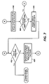
- an encoded bitstream is compressed, with compressor 62 (step 404) and then stored in EPC memory 24 (step 406).
- the compressed, encoded bitstream is, via step 408, held in the EPC memory until it is either copied to disk 34 (step not shown) or outputted to an appropriate output device, such as the printer 20.
- decompression is effected, via step 410, with the decompressor 64.
- movement of data between the image processing section, compressor, EPC memory and the decompressor is facilitated with the transfer modules 36.
- bitstream analyzing arrangement In anticipation of outputting the image data, the corresponding bitstream is analyzed, per step 412, with a bitstream analyzing arrangement.
- a bitstream analyzer Referring generally to Figures 9-13, an example of a reconstruction scheme, with a bitstream analyzer is illustrated. It will be appreciated by those skilled in the art that operation of the bitstream analyzer can be implemented with a suitable processor. Moreover, the image assumes the form of a bitmap with a plurality of scanlines.
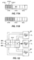
- each pixel for a given input bitstream is read for purposes of comparing bit pairs representative of "neighboring" or "framing" pixels with the entries of a 16 x 1 look-up table. More particularly, each central pixel 411a is disposed intermediate of a left neighbor pixel 411b and a right neighbor pixel 411c.
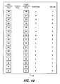
- the respective bit pairs of the left neighbor and the right neighbor, for each G 1 or G2 pixel are compared to each of sixteen bit pairs in the look-up table 415 of Figure 10. In turn, a match is obtained and a corresponding positional signal or value is assigned to the central or present pixel.
- the positional signal of the illustrated look-up table facilitates a reconstruction of the bit discarded during the encoding of the image data. More particularly, it is known that, in a typical black and white image, black pixels tend to group together. Accordingly, this knowledge can be used in reconstructing the present pixel of Figure 8 when that pixel assumes the form of the G1 pixel or the G2 pixel. It stands to reason that the gray part of a G1 or G2 central pixel would tend to associate with the neighboring pixel having the greatest intensity.
- the pixel 411b which has an intensity of 11, is referred to, in the look-up table 415 ( Figure 10), as "B" and the pixel 411c, which has an intensity of 00, is referred to, in the look-up table, as "W".
- the position of the gray pixel in the present pixel is left justified ( Figure 8) so that the one black pixel of the pixel 411a is grouped with the black pixels 411b-1, 411b-2 and 411b-3 of pixel 411b. It will be appreciated that while the current methodology groups black pixels, in another approach, white pixels could be grouped together.
- step 422 Figure 6
- step 424 where a positional signal of "0" or "1" is assigned to the central or present pixel 411.
- a single bit cannot designate each case for a GRAY1 pixel in that an 1800 x 1 pixel ( Figure 8) can assume one of three positions.
- the present technique assumes that the 1800 x 1 pixel is either left or right justified.
- center justification would be accommodated for by using two bits to describe the positional signal. It will be recognized that use of two bits to describe justification provides additional flexibility to the current technique.
- a corresponding two pixels of a previous scanline 428 are examined (step 430) with the bitstream analyzer.
- a second 16 x 1 look-up table 432 identical to the one of Figures 10 and 12, namely look-up table 415, is employed. If a match is found in the second look-up table, and the match does not relate to a bit pair in which the intensities are the same (e.g. the intensities are W-W), then a positional signal is obtained in the same manner as described for step 424.
- step 436 the intensities of a corresponding two pixels of a next scanline 438 are examined with a third look-up table 440, which third look-up table is identical in content to the first look-up table 434. If a match is found in the third look-up table, and the match does not relate to a bit pair in which the intensities are each white, then a positional signal is obtained in the same manner as described for step 424. If a match cannot be made on the basis of examining any of the scanlines 425, 428 or 438, then, via steps 444, 446, default positional value is, via step 446, assigned.
- the three scanlines are analyzed simultaneously to determine what the positional signal of the present pixel should be.
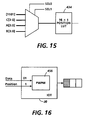
- one of a plurality of output signals from the look-up tables 415, 432 and 440 is then chosen with a 4 to 1 multiplexer 450 ( Figure 13), which multiplexer is controlled by selected signals designated as "SEL0" and SEL1".
- Figure 13 an implementation for generating the select signals is shown. Referring conjunctively to Figures 13 and 14, when the respective signals of SEL0 and SEL1 are 1 and 1, the positional signal of look-up table 415 is permitted to pass through a multiplexer 450.
- the positional signal of look-up table 432 is permitted to pass through the multiplexer 450.
- the positional signal of look-up table 440 is permitted to pass through the multiplexer 450.
- a preassigned signal e.g. a 1 is permitted to pass through the multiplexer 450. It will be appreciated that the preassigned signal may be assigned, for example, on the basis of empirical data.
- the position signal for the present pixel 423 could be obtained through the use of an arrangement with just one of the look-up tables 415, 434 or 440 and the multiplexer 450. More particularly, in this other embodiment, the bits corresponding to each of the framing or neighboring pixels of scanlines 425, 428 and 438, along with a suitable set of default bits, is transmitted to the four inputs of the multiplexer 450. Through use of appropriate select signals, from the select circuit of Figure 14, one of the bit sets is permitted to pass through the multiplexer, and, in turn, that bit set is processed with the look-up table.
- a check is performed, at step 352, to determine if all of the image data for a given input image has been processed. If an end to the image data has not been reached, then the neighboring pixels of another central pixel are examined (step 454) and the process returns to step 424. If, on the other hand, all of the image data for the given input image has been processed, then the image data of the given input image is prepared for output.
- the image data is transmitted to the printer 20, the printer 20 including a component 456 referred to as a pulse width position modulator ("PWPM").
- PWPM serves to control the operation of a raster output scanner ("ROS") as a function of digital input provided thereto.
- ROS raster output scanner
- the PWPM is responsive to the representative bits of a given pixel and, where appropriate, a positional signal so that three output pixels are reproduced by the ROS on the basis of the two or three bits provided to the PWPM.
- the output includes two white pixels and one black pixel with the black pixel being left justified.
- the present technique includes an encoding approach which permits m out of every n bits to be discarded from image data of an input image where the m bits represent "positional" bits and n - m bits correspond with 2 n-m intensities.
- This discarding of bits results in a decrease of storage demand. In one example a storage saving of up to 33% is achieved. In some cases, such as the ones in which a pixel is all white or all black, the discarded bit will not be missed. That is, in some instances, it is possible to describe, completely, the output states of n bits with just n - m bits. In any event, "lost" information provided by the discarded bits is, where necessary, reconstructed, so there is little or no loss in image output quality.
- Reconstruction is preferably accomplished by examining each pixel in an image and assigning a positional signal, when appropriate. Such reconstruction is believed to be necessary when the position of one or two black pixels, disposed in a group of three pixels cannot be positioned or justified on the basis of two bits worth of image information. Due to the assignment of the positional signals, virtually all of the information, related to the input image, can be recaptured for output.
- each positional signal is assigned with a high degree of accuracy.
- a pixel being examined is framed by two pixels of the same intensity, e.g. white pixels
- corresponding pixels from adjacent scanlines are analyzed to optimize eventual justification of one or more black pixels.
- the examined pixels of the multiple scanlines can be analyzed in parallel so that the best suited positional signal can be obtained within a relatively short time interval.
Landscapes
- Engineering & Computer Science (AREA)
- Multimedia (AREA)
- Signal Processing (AREA)
- Image Processing (AREA)
- Record Information Processing For Printing (AREA)
- Processing Or Creating Images (AREA)
Applications Claiming Priority (2)
| Application Number | Priority Date | Filing Date | Title |
|---|---|---|---|
| US08/315,275 US5659634A (en) | 1994-09-29 | 1994-09-29 | Apparatus and method for encoding and reconstructing image data |
| US315275 | 1994-09-29 |
Publications (2)
| Publication Number | Publication Date |
|---|---|
| EP0705026A1 true EP0705026A1 (fr) | 1996-04-03 |
| EP0705026B1 EP0705026B1 (fr) | 2001-12-12 |
Family
ID=23223663
Family Applications (1)
| Application Number | Title | Priority Date | Filing Date |
|---|---|---|---|
| EP95306903A Expired - Lifetime EP0705026B1 (fr) | 1994-09-29 | 1995-09-29 | Appareil et procédé pour le codage et la reconstruction de données d'image |
Country Status (4)
| Country | Link |
|---|---|
| US (1) | US5659634A (fr) |
| EP (1) | EP0705026B1 (fr) |
| JP (1) | JPH08112947A (fr) |
| DE (1) | DE69524520T2 (fr) |
Cited By (3)
| Publication number | Priority date | Publication date | Assignee | Title |
|---|---|---|---|---|
| EP1202556A3 (fr) * | 2000-09-27 | 2002-07-17 | Ricoh Company, Ltd. | Appareil et procédé de traitement d'image et support d'enregistrement |
| WO2005091616A1 (fr) * | 2004-03-17 | 2005-09-29 | Hewlett-Packard Development Company L.P. | Diffusion d'erreurs utilisant une modulation de sous-pixels |
| US7782326B2 (en) | 2004-02-25 | 2010-08-24 | Marvell International Technology Ltd. | Parallel video processing architecture |
Families Citing this family (17)
| Publication number | Priority date | Publication date | Assignee | Title |
|---|---|---|---|---|
| JP2001502503A (ja) * | 1996-10-11 | 2001-02-20 | サーノフ コーポレイション | ビットストリーム解析のための装置及び方法 |
| US5986714A (en) * | 1997-06-10 | 1999-11-16 | International Business Machines Corporation | Method, apparatus and computer program product for selectively reducing bandwidth of real-time video data |
| US6141114A (en) * | 1998-01-08 | 2000-10-31 | Xerox Corporation | Edge enhanced error diffusion with artifact correction in areas of highlights and shadows |
| US6437872B1 (en) * | 1998-09-22 | 2002-08-20 | Xerox Corporation | Multibit screening of print documents in a PDL environment |
| US6266157B1 (en) | 1998-11-13 | 2001-07-24 | Xerox Corporation | Method of error diffusion using 2×2 color correction and increment matching |
| US6285462B1 (en) | 1998-11-13 | 2001-09-04 | Xerox Corporation | Intelligent GCR/UCR process to reduce multiple colorant moire in color printing |
| US6356654B1 (en) | 1998-12-23 | 2002-03-12 | Xerox Corporation | Systems and methods for template matching of multicolored images |
| US6343159B1 (en) | 1998-12-23 | 2002-01-29 | Xerox Corporation | Method and apparatus for modeling and reconstruction of halftoned images |
| US6363177B1 (en) | 1998-12-30 | 2002-03-26 | Xerox Corporation | Systems and methods for rotating high addressability images |
| US6301397B1 (en) | 1998-12-30 | 2001-10-09 | Xerox Corporation | Systems and methods for rotating high addressability images |
| US6381372B1 (en) | 1998-12-30 | 2002-04-30 | Xerox Corporation | Systems and methods for designing image processing filters using templates |
| US6683702B1 (en) * | 1999-07-07 | 2004-01-27 | Xerox Corporation | Compact-dot reproduction of scanned halftone screens |
| US7496234B2 (en) * | 2003-06-20 | 2009-02-24 | Microsoft Corporation | System and method for seamless multiplexing of embedded bitstreams |
| US7738710B2 (en) * | 2004-08-02 | 2010-06-15 | Electronics For Imaging, Inc. | Methods and apparatus for communicating and displaying compressed image data |
| US7852531B2 (en) * | 2007-12-12 | 2010-12-14 | Xerox Corporation | Digital correction for alignment of a plurality of color channels of a color image forming device |
| US10158784B2 (en) | 2016-12-07 | 2018-12-18 | Xerox Corporation | System and method for adaptively compressing data having noisy images using lossless compression |
| JP2024521572A (ja) * | 2021-06-08 | 2024-06-03 | オーピー ソリューションズ, エルエルシー | 組み合わせられた可逆符号化および非可逆符号化のための機械向け映像符号化(vcm)エンコーダおよびデコーダ |
Citations (6)
| Publication number | Priority date | Publication date | Assignee | Title |
|---|---|---|---|---|
| US4124870A (en) * | 1977-03-31 | 1978-11-07 | International Business Machines Corporation | Method for improving print quality of coarse-scan/fine-print character reproduction |
| WO1981002206A1 (fr) * | 1980-01-26 | 1981-08-06 | Hell R Gmbh | Procede pour obtenir une meilleure restitution d'images dans la technique de reproduction |
| EP0109005A1 (fr) * | 1982-11-08 | 1984-05-23 | International Business Machines Corporation | Procédé fournissant une image en demi-tons |
| EP0132455A1 (fr) * | 1983-07-29 | 1985-02-13 | DR.-ING. RUDOLF HELL GmbH | Procédé et appareil pour la représentation de lignes graphiques à haute définition |
| EP0220568A2 (fr) * | 1985-11-01 | 1987-05-06 | Dainippon Screen Mfg. Co., Ltd. | Procédé et appareil de génération de données d'image à deux niveaux et à haute définition |
| US5170340A (en) | 1990-09-28 | 1992-12-08 | Xerox Corporation | System state controller for electronic image processing systems |
Family Cites Families (19)
| Publication number | Priority date | Publication date | Assignee | Title |
|---|---|---|---|---|
| US3597071A (en) * | 1968-08-30 | 1971-08-03 | Xerox Corp | Diverse-input system for electrostatically reproducing and recording information |
| CA1086231A (fr) * | 1976-03-08 | 1980-09-23 | Lee N. Davy | Appareil de reproduction de documents a memoire d'interclassement electronique |
| US4558370A (en) * | 1983-11-21 | 1985-12-10 | International Business Machines Corporation | Image processing method for graphics images |
| JPS6162286A (ja) * | 1984-09-04 | 1986-03-31 | Univ Nagoya | 画像信号帯域圧縮方式 |
| US4742550A (en) * | 1984-09-17 | 1988-05-03 | Motorola, Inc. | 4800 BPS interoperable relp system |
| JP2733220B2 (ja) * | 1986-09-30 | 1998-03-30 | シャープ株式会社 | 複合型画像処理装置 |
| US4821107A (en) * | 1987-01-26 | 1989-04-11 | Minolta Camera Kabushiki Kaisha | Multi-functional imaging apparatus |
| US5047955A (en) * | 1987-06-19 | 1991-09-10 | Eastman Kodak Company | Electronic collation |
| JPH01195770A (ja) * | 1988-01-29 | 1989-08-07 | Yokogawa Hewlett Packard Ltd | 画像データ圧縮伝送方法 |
| US4847677A (en) * | 1988-04-27 | 1989-07-11 | Universal Video Communications Corp. | Video telecommunication system and method for compressing and decompressing digital color video data |
| US5056154A (en) * | 1988-11-07 | 1991-10-08 | Sharp Kabushiki Kaisha | Text image data compression system |
| US5237316A (en) * | 1990-02-02 | 1993-08-17 | Washington University | Video display with high speed reconstruction and display of compressed images at increased pixel intensity range and retrofit kit for same |
| US5305159A (en) * | 1990-08-08 | 1994-04-19 | Kabushiki Kaisha Toshiba | Magnetic disk apparatus |
| US5301262A (en) * | 1990-10-10 | 1994-04-05 | Fuji Xerox Co., Ltd. | Image processor |
| US5175633A (en) * | 1990-10-10 | 1992-12-29 | Fuji Xerox Co., Ltd. | Method of diagnosing operating conditions of an image processor |
| US5223948A (en) * | 1990-10-10 | 1993-06-29 | Fuji Xerox Co., Ltd. | Image processing apparatus |
| US5276799A (en) * | 1991-10-29 | 1994-01-04 | Xerox Corporation | Expandable electronic subsystem for a printing machine |
| US5307458A (en) * | 1991-12-23 | 1994-04-26 | Xerox Corporation | Input/output coprocessor for printing machine |
| JPH05191608A (ja) * | 1992-01-08 | 1993-07-30 | Canon Inc | カラー画像形成装置 |
-
1994
- 1994-09-29 US US08/315,275 patent/US5659634A/en not_active Expired - Lifetime
-
1995
- 1995-09-20 JP JP7241224A patent/JPH08112947A/ja not_active Withdrawn
- 1995-09-29 EP EP95306903A patent/EP0705026B1/fr not_active Expired - Lifetime
- 1995-09-29 DE DE69524520T patent/DE69524520T2/de not_active Expired - Lifetime
Patent Citations (6)
| Publication number | Priority date | Publication date | Assignee | Title |
|---|---|---|---|---|
| US4124870A (en) * | 1977-03-31 | 1978-11-07 | International Business Machines Corporation | Method for improving print quality of coarse-scan/fine-print character reproduction |
| WO1981002206A1 (fr) * | 1980-01-26 | 1981-08-06 | Hell R Gmbh | Procede pour obtenir une meilleure restitution d'images dans la technique de reproduction |
| EP0109005A1 (fr) * | 1982-11-08 | 1984-05-23 | International Business Machines Corporation | Procédé fournissant une image en demi-tons |
| EP0132455A1 (fr) * | 1983-07-29 | 1985-02-13 | DR.-ING. RUDOLF HELL GmbH | Procédé et appareil pour la représentation de lignes graphiques à haute définition |
| EP0220568A2 (fr) * | 1985-11-01 | 1987-05-06 | Dainippon Screen Mfg. Co., Ltd. | Procédé et appareil de génération de données d'image à deux niveaux et à haute définition |
| US5170340A (en) | 1990-09-28 | 1992-12-08 | Xerox Corporation | System state controller for electronic image processing systems |
Cited By (6)
| Publication number | Priority date | Publication date | Assignee | Title |
|---|---|---|---|---|
| EP1202556A3 (fr) * | 2000-09-27 | 2002-07-17 | Ricoh Company, Ltd. | Appareil et procédé de traitement d'image et support d'enregistrement |
| US7027190B2 (en) | 2000-09-27 | 2006-04-11 | Ricoh Company, Ltd. | Image-processing apparatus, image-processing method and recording medium |
| US7545538B2 (en) | 2000-09-27 | 2009-06-09 | Ricoh Company, Ltd. | Image-processing apparatus, image-processing method and recording medium |
| US7782326B2 (en) | 2004-02-25 | 2010-08-24 | Marvell International Technology Ltd. | Parallel video processing architecture |
| US8098252B2 (en) | 2004-02-25 | 2012-01-17 | Marvell International Technology Ltd. | Parallel video processing architecture |
| WO2005091616A1 (fr) * | 2004-03-17 | 2005-09-29 | Hewlett-Packard Development Company L.P. | Diffusion d'erreurs utilisant une modulation de sous-pixels |
Also Published As
| Publication number | Publication date |
|---|---|
| DE69524520D1 (de) | 2002-01-24 |
| JPH08112947A (ja) | 1996-05-07 |
| US5659634A (en) | 1997-08-19 |
| DE69524520T2 (de) | 2002-05-23 |
| EP0705026B1 (fr) | 2001-12-12 |
Similar Documents
| Publication | Publication Date | Title |
|---|---|---|
| EP0705026B1 (fr) | Appareil et procédé pour le codage et la reconstruction de données d'image | |
| EP0704791A1 (fr) | Méthode de traitement de tâche dans un système d'impression avec un ticket de tâche composite | |
| EP0704792B1 (fr) | Méthode de gestion d'allocation de mémoire dans un système d'impression | |
| EP1193610B1 (fr) | Dispositif de traitement de données et méthode de transfert de données DMA | |
| US5627658A (en) | Automatic networked facsimile queuing system | |
| US7123385B2 (en) | Image processing apparatus | |
| EP0705023B1 (fr) | Appareil pour maximaliser le débit de transfert de données d'image dans un système d'impression | |
| US6900909B2 (en) | Image processor | |
| JPH0934824A (ja) | ジョブチケットを用いた画像処理装置及び方法 | |
| US5574834A (en) | Image communication system for following a communication procedure to simultaneously transmit image code data | |
| JPH08331372A (ja) | イメージ信号の非整数の解像度変換を行う方法 | |
| JPH08115414A (ja) | 差込み/注釈付け/背丁付け能力を有する印刷機械 | |
| EP1104172B1 (fr) | Procédé et appareil permettant le traitement de tâches en continu pour un jeu de ressources partagées en commun | |
| EP1104171A2 (fr) | Procédé et appareil d'optimisation de transition de resources à partir d'une priorité de tâche plus basse vers une une priorité plus élevée | |
| US5970222A (en) | Memory management system for printing a print job with limited capacity | |
| US5606648A (en) | Apparatus and method for modulating image signals in a high addressability printing machine | |
| EP1104169A2 (fr) | Procédé et appareil pour permettre le traitement de plusieurs capacités pour une sous-tâche pendant l'utilisation d'un jeu de resources partagées en commun | |
| JP4027133B2 (ja) | 画像処理装置 | |
| CA2215656C (fr) | Systeme d'impression a fonction de programmation de taches d'impression | |
| US5668938A (en) | Control system for programming first print out time in a printing system | |
| US6981069B2 (en) | Compressed data transmission over a plurality of transmission paths | |
| JPH1070648A (ja) | 印刷装置及び印刷方法 | |
| US5706409A (en) | Image shifting system for use in a document processing system | |
| US6449059B1 (en) | Interface device and image forming apparatus | |
| WO1988006768A1 (fr) | Processeur d'images de canevas a vitesse elevee |
Legal Events
| Date | Code | Title | Description |
|---|---|---|---|
| PUAI | Public reference made under article 153(3) epc to a published international application that has entered the european phase |
Free format text: ORIGINAL CODE: 0009012 |
|
| AK | Designated contracting states |
Kind code of ref document: A1 Designated state(s): DE FR GB |
|
| 17P | Request for examination filed |
Effective date: 19961004 |
|
| 17Q | First examination report despatched |
Effective date: 19981013 |
|
| GRAG | Despatch of communication of intention to grant |
Free format text: ORIGINAL CODE: EPIDOS AGRA |
|
| GRAG | Despatch of communication of intention to grant |
Free format text: ORIGINAL CODE: EPIDOS AGRA |
|
| GRAH | Despatch of communication of intention to grant a patent |
Free format text: ORIGINAL CODE: EPIDOS IGRA |
|
| GRAH | Despatch of communication of intention to grant a patent |
Free format text: ORIGINAL CODE: EPIDOS IGRA |
|
| GRAA | (expected) grant |
Free format text: ORIGINAL CODE: 0009210 |
|
| AK | Designated contracting states |
Kind code of ref document: B1 Designated state(s): DE FR GB |
|
| REG | Reference to a national code |
Ref country code: GB Ref legal event code: IF02 |
|
| REF | Corresponds to: |
Ref document number: 69524520 Country of ref document: DE Date of ref document: 20020124 |
|
| ET | Fr: translation filed |
Owner name: DEUTSCHE TELEKOM AG Owner name: KONINKLIJKE PHILIPS ELECTRONICS N.V. |
|
| PLBE | No opposition filed within time limit |
Free format text: ORIGINAL CODE: 0009261 |
|
| STAA | Information on the status of an ep patent application or granted ep patent |
Free format text: STATUS: NO OPPOSITION FILED WITHIN TIME LIMIT |
|
| 26N | No opposition filed |
Opponent name: DEUTSCHE TELEKOM AG Opponent name: KONINKLIJKE PHILIPS ELECTRONICS N.V. |
|
| REG | Reference to a national code |
Ref country code: GB Ref legal event code: 746 Effective date: 20050512 |
|
| PGFP | Annual fee paid to national office [announced via postgrant information from national office to epo] |
Ref country code: DE Payment date: 20130820 Year of fee payment: 19 |
|
| PGFP | Annual fee paid to national office [announced via postgrant information from national office to epo] |
Ref country code: GB Payment date: 20130823 Year of fee payment: 19 |
|
| PGFP | Annual fee paid to national office [announced via postgrant information from national office to epo] |
Ref country code: FR Payment date: 20130920 Year of fee payment: 19 |
|
| REG | Reference to a national code |
Ref country code: DE Ref legal event code: R119 Ref document number: 69524520 Country of ref document: DE |
|
| GBPC | Gb: european patent ceased through non-payment of renewal fee |
Effective date: 20140929 |
|
| REG | Reference to a national code |
Ref country code: FR Ref legal event code: ST Effective date: 20150529 |
|
| PG25 | Lapsed in a contracting state [announced via postgrant information from national office to epo] |
Ref country code: GB Free format text: LAPSE BECAUSE OF NON-PAYMENT OF DUE FEES Effective date: 20140929 Ref country code: DE Free format text: LAPSE BECAUSE OF NON-PAYMENT OF DUE FEES Effective date: 20150401 |
|
| PG25 | Lapsed in a contracting state [announced via postgrant information from national office to epo] |
Ref country code: FR Free format text: LAPSE BECAUSE OF NON-PAYMENT OF DUE FEES Effective date: 20140930 |