EP0707305A2 - Anzeigemodusdetektor, Bildelementtaktsynchronisator und Interpolator für eine ferroelektrische Flüssigkristallanzeige - Google Patents
Anzeigemodusdetektor, Bildelementtaktsynchronisator und Interpolator für eine ferroelektrische Flüssigkristallanzeige Download PDFInfo
- Publication number
- EP0707305A2 EP0707305A2 EP95116047A EP95116047A EP0707305A2 EP 0707305 A2 EP0707305 A2 EP 0707305A2 EP 95116047 A EP95116047 A EP 95116047A EP 95116047 A EP95116047 A EP 95116047A EP 0707305 A2 EP0707305 A2 EP 0707305A2
- Authority
- EP
- European Patent Office
- Prior art keywords
- display
- signal
- video signal
- display mode
- clock signal
- Prior art date
- Legal status (The legal status is an assumption and is not a legal conclusion. Google has not performed a legal analysis and makes no representation as to the accuracy of the status listed.)
- Withdrawn
Links
Images



Classifications
-
- G—PHYSICS
- G06—COMPUTING OR CALCULATING; COUNTING
- G06T—IMAGE DATA PROCESSING OR GENERATION, IN GENERAL
- G06T3/00—Geometric image transformations in the plane of the image
- G06T3/40—Scaling of whole images or parts thereof, e.g. expanding or contracting
- G06T3/4007—Scaling of whole images or parts thereof, e.g. expanding or contracting based on interpolation, e.g. bilinear interpolation
-
- G—PHYSICS
- G06—COMPUTING OR CALCULATING; COUNTING
- G06T—IMAGE DATA PROCESSING OR GENERATION, IN GENERAL
- G06T3/00—Geometric image transformations in the plane of the image
- G06T3/40—Scaling of whole images or parts thereof, e.g. expanding or contracting
- G06T3/4092—Image resolution transcoding, e.g. by using client-server architectures
-
- G—PHYSICS
- G09—EDUCATION; CRYPTOGRAPHY; DISPLAY; ADVERTISING; SEALS
- G09G—ARRANGEMENTS OR CIRCUITS FOR CONTROL OF INDICATING DEVICES USING STATIC MEANS TO PRESENT VARIABLE INFORMATION
- G09G5/00—Control arrangements or circuits for visual indicators common to cathode-ray tube indicators and other visual indicators
- G09G5/003—Details of a display terminal, the details relating to the control arrangement of the display terminal and to the interfaces thereto
- G09G5/005—Adapting incoming signals to the display format of the display terminal
-
- H—ELECTRICITY
- H03—ELECTRONIC CIRCUITRY
- H03L—AUTOMATIC CONTROL, STARTING, SYNCHRONISATION OR STABILISATION OF GENERATORS OF ELECTRONIC OSCILLATIONS OR PULSES
- H03L7/00—Automatic control of frequency or phase; Synchronisation
- H03L7/06—Automatic control of frequency or phase; Synchronisation using a reference signal applied to a frequency- or phase-locked loop
- H03L7/08—Details of the phase-locked loop
- H03L7/099—Details of the phase-locked loop concerning mainly the controlled oscillator of the loop
-
- G—PHYSICS
- G09—EDUCATION; CRYPTOGRAPHY; DISPLAY; ADVERTISING; SEALS
- G09G—ARRANGEMENTS OR CIRCUITS FOR CONTROL OF INDICATING DEVICES USING STATIC MEANS TO PRESENT VARIABLE INFORMATION
- G09G2300/00—Aspects of the constitution of display devices
- G09G2300/04—Structural and physical details of display devices
- G09G2300/0404—Matrix technologies
- G09G2300/0408—Integration of the drivers onto the display substrate
-
- G—PHYSICS
- G09—EDUCATION; CRYPTOGRAPHY; DISPLAY; ADVERTISING; SEALS
- G09G—ARRANGEMENTS OR CIRCUITS FOR CONTROL OF INDICATING DEVICES USING STATIC MEANS TO PRESENT VARIABLE INFORMATION
- G09G2310/00—Command of the display device
- G09G2310/02—Addressing, scanning or driving the display screen or processing steps related thereto
- G09G2310/0202—Addressing of scan or signal lines
- G09G2310/0205—Simultaneous scanning of several lines in flat panels
-
- G—PHYSICS
- G09—EDUCATION; CRYPTOGRAPHY; DISPLAY; ADVERTISING; SEALS
- G09G—ARRANGEMENTS OR CIRCUITS FOR CONTROL OF INDICATING DEVICES USING STATIC MEANS TO PRESENT VARIABLE INFORMATION
- G09G2310/00—Command of the display device
- G09G2310/02—Addressing, scanning or driving the display screen or processing steps related thereto
- G09G2310/0224—Details of interlacing
-
- G—PHYSICS
- G09—EDUCATION; CRYPTOGRAPHY; DISPLAY; ADVERTISING; SEALS
- G09G—ARRANGEMENTS OR CIRCUITS FOR CONTROL OF INDICATING DEVICES USING STATIC MEANS TO PRESENT VARIABLE INFORMATION
- G09G2310/00—Command of the display device
- G09G2310/04—Partial updating of the display screen
-
- G—PHYSICS
- G09—EDUCATION; CRYPTOGRAPHY; DISPLAY; ADVERTISING; SEALS
- G09G—ARRANGEMENTS OR CIRCUITS FOR CONTROL OF INDICATING DEVICES USING STATIC MEANS TO PRESENT VARIABLE INFORMATION
- G09G2320/00—Control of display operating conditions
- G09G2320/02—Improving the quality of display appearance
- G09G2320/0271—Adjustment of the gradation levels within the range of the gradation scale, e.g. by redistribution or clipping
- G09G2320/0276—Adjustment of the gradation levels within the range of the gradation scale, e.g. by redistribution or clipping for the purpose of adaptation to the characteristics of a display device, i.e. gamma correction
-
- G—PHYSICS
- G09—EDUCATION; CRYPTOGRAPHY; DISPLAY; ADVERTISING; SEALS
- G09G—ARRANGEMENTS OR CIRCUITS FOR CONTROL OF INDICATING DEVICES USING STATIC MEANS TO PRESENT VARIABLE INFORMATION
- G09G2340/00—Aspects of display data processing
- G09G2340/04—Changes in size, position or resolution of an image
- G09G2340/0407—Resolution change, inclusive of the use of different resolutions for different screen areas
- G09G2340/0414—Vertical resolution change
-
- G—PHYSICS
- G09—EDUCATION; CRYPTOGRAPHY; DISPLAY; ADVERTISING; SEALS
- G09G—ARRANGEMENTS OR CIRCUITS FOR CONTROL OF INDICATING DEVICES USING STATIC MEANS TO PRESENT VARIABLE INFORMATION
- G09G2340/00—Aspects of display data processing
- G09G2340/04—Changes in size, position or resolution of an image
- G09G2340/0407—Resolution change, inclusive of the use of different resolutions for different screen areas
- G09G2340/0421—Horizontal resolution change
-
- G—PHYSICS
- G09—EDUCATION; CRYPTOGRAPHY; DISPLAY; ADVERTISING; SEALS
- G09G—ARRANGEMENTS OR CIRCUITS FOR CONTROL OF INDICATING DEVICES USING STATIC MEANS TO PRESENT VARIABLE INFORMATION
- G09G2340/00—Aspects of display data processing
- G09G2340/04—Changes in size, position or resolution of an image
- G09G2340/0464—Positioning
-
- G—PHYSICS
- G09—EDUCATION; CRYPTOGRAPHY; DISPLAY; ADVERTISING; SEALS
- G09G—ARRANGEMENTS OR CIRCUITS FOR CONTROL OF INDICATING DEVICES USING STATIC MEANS TO PRESENT VARIABLE INFORMATION
- G09G2340/00—Aspects of display data processing
- G09G2340/04—Changes in size, position or resolution of an image
- G09G2340/0464—Positioning
- G09G2340/0478—Horizontal positioning
-
- G—PHYSICS
- G09—EDUCATION; CRYPTOGRAPHY; DISPLAY; ADVERTISING; SEALS
- G09G—ARRANGEMENTS OR CIRCUITS FOR CONTROL OF INDICATING DEVICES USING STATIC MEANS TO PRESENT VARIABLE INFORMATION
- G09G3/00—Control arrangements or circuits, of interest only in connection with visual indicators other than cathode-ray tubes
- G09G3/20—Control arrangements or circuits, of interest only in connection with visual indicators other than cathode-ray tubes for presentation of an assembly of a number of characters, e.g. a page, by composing the assembly by combination of individual elements arranged in a matrix no fixed position being assigned to or needed to be assigned to the individual characters or partial characters
- G09G3/34—Control arrangements or circuits, of interest only in connection with visual indicators other than cathode-ray tubes for presentation of an assembly of a number of characters, e.g. a page, by composing the assembly by combination of individual elements arranged in a matrix no fixed position being assigned to or needed to be assigned to the individual characters or partial characters by control of light from an independent source
- G09G3/36—Control arrangements or circuits, of interest only in connection with visual indicators other than cathode-ray tubes for presentation of an assembly of a number of characters, e.g. a page, by composing the assembly by combination of individual elements arranged in a matrix no fixed position being assigned to or needed to be assigned to the individual characters or partial characters by control of light from an independent source using liquid crystals
- G09G3/3611—Control of matrices with row and column drivers
- G09G3/3622—Control of matrices with row and column drivers using a passive matrix
- G09G3/3629—Control of matrices with row and column drivers using a passive matrix using liquid crystals having memory effects, e.g. ferroelectric liquid crystals
-
- G—PHYSICS
- G09—EDUCATION; CRYPTOGRAPHY; DISPLAY; ADVERTISING; SEALS
- G09G—ARRANGEMENTS OR CIRCUITS FOR CONTROL OF INDICATING DEVICES USING STATIC MEANS TO PRESENT VARIABLE INFORMATION
- G09G5/00—Control arrangements or circuits for visual indicators common to cathode-ray tube indicators and other visual indicators
- G09G5/003—Details of a display terminal, the details relating to the control arrangement of the display terminal and to the interfaces thereto
- G09G5/006—Details of the interface to the display terminal
-
- G—PHYSICS
- G09—EDUCATION; CRYPTOGRAPHY; DISPLAY; ADVERTISING; SEALS
- G09G—ARRANGEMENTS OR CIRCUITS FOR CONTROL OF INDICATING DEVICES USING STATIC MEANS TO PRESENT VARIABLE INFORMATION
- G09G5/00—Control arrangements or circuits for visual indicators common to cathode-ray tube indicators and other visual indicators
- G09G5/003—Details of a display terminal, the details relating to the control arrangement of the display terminal and to the interfaces thereto
- G09G5/006—Details of the interface to the display terminal
- G09G5/008—Clock recovery
-
- G—PHYSICS
- G09—EDUCATION; CRYPTOGRAPHY; DISPLAY; ADVERTISING; SEALS
- G09G—ARRANGEMENTS OR CIRCUITS FOR CONTROL OF INDICATING DEVICES USING STATIC MEANS TO PRESENT VARIABLE INFORMATION
- G09G5/00—Control arrangements or circuits for visual indicators common to cathode-ray tube indicators and other visual indicators
- G09G5/18—Timing circuits for raster scan displays
Definitions
- the present invention relates to a display device for displaying an image on a screen, and a display control method and apparatus therefor.
- a flat panel display using, e.g., a liquid crystal has recently received a lot of attention. It is expected that such a flat panel display be used as a display monitor not only for lap-top computers and notebook computers but also for desktop computers due to its compact structure and very low radiation of electromagnetic waves in place of CRT displays used so far.
- a display using a ferroelectric liquid crystal (FLC) (to be abbreviated as an FLCD hereinafter) is commercially available.
- FLCD ferroelectric liquid crystal
- Such an FLCD has a nature called a memory characteristic (i.e., a nature that maintains the ON/OFF states of liquid crystal pixels after an electric field required for turning on/off the pixels to be displayed is removed), and by utilizing this characteristic, a large-screen of flat panel display, which is very difficult to attain by the conventional liquid crystal technique, can be realized. More specifically, by using a partial rewrite scanning mode for selectively scanning only lines of changed image data to be displayed, the screen can be efficiently refreshed.
- the display operation is realized as follows. That is, when the number of display pixels of the FLCD is equal to the number of pixels output from the computer, i.e., is 1,280 x 1,024, image and synchronizing signal are received from the computer, and horizontal and vertical synchronizing signals are separated from the synchronizing signal. Using the separated horizontal synchronizing signal, FLCD dot clock signal synchronized with the pixel clocks of the computer is reproduced, and the image signal is A/D (analog-to-digital) converted using the FLCD dot clock signal. The converted digital data is subjected to ⁇ characteristic adjustment and halftone processing.
- the digital image data is transferred to an output controller of the FLCD, thus displaying an image.
- the timings of the horizontal and vertical synchronizing signals and the dot clock signal synchronized with displaying pixels are peculiar to each computer. For this reason, using an FLCD interface board depending on a computer to be connected, image data from the computer can be displayed on the FLCD.
- the present invention has been made in consideration of the above situation, and has as its object to provide a display device which can display an image in correspondence with various display modes, and a display control method and apparatus therefor.
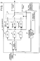
- Fig. 1 is a block diagram showing the arrangement of a display control apparatus according to an embodiment of the present invention.
- reference numeral 1 denotes a display interface; 2, a video signal processor; 3, a digital image processor; and 4, an FLC display unit.
- Reference numeral 11 denotes an input terminal for receiving an RGB signal from, e.g., a computer 100 such as a workstation, a personal computer, or the like; 12, a terminal for receiving an image synchronizing signal from, e.g., the computer 100 as in the input terminal 11.
- the video and synchronizing signals output from the computer 100 are input to and processed by the display interface 1, and thereafter, an image is displayed on the display unit 4.
- a display mode detector 15 receives vertical and horizontal synchronizing signals in the computer synchronizing signal input from the terminal 12, and discriminates the current display mode on the basis of the timings, polarities, and the like of these synchronizing signals.
- the display mode detector 15 supplies the detection result to a display mode dependence controller 17.
- a clock generator 14 receives a horizontal synchronizing signal in the synchronizing signal supplied from the computer 100, and generates a dot clock signal 41 in accordance with the discrimination result of the display mode supplied from the display mode dependence controller 17.
- An ADC (A/D converter) 13 samples an RGB analog signal input from the input terminal 11 at the timing of the dot clock signal 41 supplied from the clock generator 14 to generate a quantized digital RGB image data including 1,280 pixels per line.
- An interpolation processing circuit 16 expands the image defined by the input digital RGB image data input from the ADC 13 in the vertical direction in correspondence with the display mode.
- the interpolation processing circuit 16 comprises a line buffer or a frame buffer, and obtains an average of two adjacent pixels as a pixel value therebetween by a linear interpolation method.
- the interpolation processing circuit 16 may adopt other interpolation methods in consideration of the cost/performance. Whether or not interpolation of an image in the vertical direction is performed is designated by the display mode dependence controller 17.
- an RGB video signal input from the input terminal 11 normally includes characteristics for canceling the characteristics.
- a ⁇ characteristic adjustment circuit 19 adjusts the characteristics included in the RGB image data in correspondence with those of an FLCD panel 24 of the display unit 4, so as to obtain an appropriate luminance on the FLCD panel 24.
- the ⁇ characteristic adjustment circuit 19 comprises an LUT (look-up table) using a high-speed SRAM, and is set by the display mode dependence controller 17.
- a halftone processing circuit 21 performs halftone processing (e.g., dither processing) for the image data supplied from the ⁇ characteristic adjustment circuit 19.
- a frame change detector 20 compares digital image data supplied from the interpolation processing circuit 16 in units of frames, so as to detect changed lines of the image data between frames, and supplies the detection result to a scanning control circuit 22.
- the scanning control circuit 22 instructs the display unit 4 to display image data subjected to the halftone processing in the halftone processing circuit 21 on the screen (1,280 x 1,024) of the FLCD panel 24. More specifically, the circuit 22 outputs the line number of a line to be displayed, and then, transfers image data for the line. Thereafter, upon reception of the end message of displaying of the line, the circuit 22 transfers of the line number of the next line to be displayed and image data for the line. Furthermore, the circuit 22 generates a signal for instructing to perform a two-line simultaneous driving operation, as needed.
- the scanning control circuit 22 changes the scanning method as follows in accordance with an instruction from the display mode dependence controller 17 in correspondence with the display mode.
- the circuit 22 preferentially scans a changed line detected by the frame change detector 20 on the basis of interlace scanning while performing the two-line simultaneous driving operation.
- the circuit 22 performs a normal one-line driving operation on the basis of an interlace scanning, and preferentially scans a changed line detected by the frame change detector 20 in image data subjected to the interpolation processing.
- VGA or SVGA mode is controlled to display an image at substantially the center of the FLCD panel 24 since the number of pixels displayed on the FLCD panel 24 is 1,280 x 960.
- a display controller 23 displays the image data of a line designated by the scanning control circuit 22 on the FLCD panel 24.
- Fig. 2 is a block diagram showing the arrangement of the clock generator 14 of this embodiment.
- Reference numeral 32 denotes a phase comparator which detects the phase difference between a horizontal synchronizing signal 31 input from the computer 100 and a signal supplied from a programmable frequency divider 40.
- a VCO (Voltage Controlled Oscillator) 36 and VCXOs 37 and 38 are oscillators for generating dot clock signal 41 in correspondence with each display mode.
- LPFs 33 to 35 are low-pass filters having a high-input impedance, each of which filters a frequency signal in corresponding to each of the horizontal frequencies of the respective display modes.
- Reference numeral 39 denotes a selection switch which comprises a circuit that allows a high-speed operation, such as a low-impedance analog switch, an ECL, or the like. The switch 39 selects one of the outputs from the VCOs (36 to 38) in response to a selection signal 42 supplied from the display mode dependence controller 17, and outputs the selected outputs as the dot clock signal 41.
- Fig. 3 is a timing chart showing the relationship between the video signal and the dot clock signal 41.
- a frequency division value 43 of the programmable frequency divider 40 is determined and set by the display mode dependence controller 17 so as to generate 1,280 clocks corresponding to the horizontal resolution of the FLCD panel 24 during the horizontal display period, as shown in Fig. 3.
- the display mode dependence controller 17 supplies control signals to the video signal processor 2 and the digital image processor 3 in accordance with the discrimination result of the display mode detector 15, as described above.
- the frequency of the dot clock signal 41 is 50 MHz. Since the number of being capable of displaying pixels (1280) in the horizontal direction of the FLCD panel 24 is twice the number of input pixels, the number of pixels to be displayed in the vertical direction is similarly doubled to maintain the aspect ratio. In this case, a control signal for performing the two-line simultaneous driving operation is supplied to the scanning control circuit 22.
- the frequency of the dot clock signal 41 is 81.3 MHz (as shown in Fig. 4). Since the number of display pixels in the horizontal direction of the FLCD panel 24 is 1.25 times the number of input pixels, the number of pixels to be displayed in the vertical direction is also multiplied with 1.25 to maintain the aspect ratio, as in the VGA mode. In this case, image data is enlarged in the vertical direction by the interpolation processing circuit 16.
- the display mode dependence controller 17 supplies a vertical interpolation control signal 26 corresponding to the current mode to the interpolation processing circuit 16.
- the display mode dependence controller 17 supplies control signals to the video signal processor 2 and the digital image processor 3 in response to a display position fine adjustment signal 18 input by a user. For example, since the horizontal displaying period differs if the frequency of the pixel clock signal varies, the width of an image is enlarged or reduced.
- the frequency of the dot clock signal 41 must be changed, and the frequency division value 43 of the programmable frequency divider 40 is changed in correspondence with the user's fine adjustment (signal 18).
- the display mode dependence controller 17 supplies a control signal for changing the timing of transfer of image data to the scanning control circuit 22 in response to the user's fine adjustment signal 18.
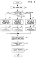
- Fig. 5 is a flow chart showing the processing of the display mode dependence controller 17 of this embodiment.
- step S2 When the controller 17 receives display mode information detected by and output from the display mode detector 15 in step S1, the flow advances to step S2 to discriminate the detected display mode. If the detected display mode is the VGA mode (640 x 480), the flow advances to step S3, and the controller 17 switches the selection switch 39 to select the LPF 33 and the VCO 36 in the clock generator 14. Then, the controller 17 sets the frequency division value 43 for outputting the dot clock signal 41 of 50 MHz in correspondence with the frequency of 31.5 kHz of the horizontal synchronizing signal in the programmable frequency divider 40. In step S4, the controller 17 instructs the interpolation processing circuit 16 to perform x2 interpolation.
- step S5 the controller 17 switches the selection switch 39 to select the LPF 34 and the VCXO 37 in the clock generator 14. Then, the controller 17 sets the frequency division value 43 for outputting the dot clock signal 41 of 64 MHz in correspondence with the frequency of 37.8 kHz of the horizontal synchronizing signal in the programmable frequency divider 40.
- step S6 the controller 17 instructs the interpolation processing circuit 16 to perform x1.6 interpolation.
- step S7 the controller 17 switches the selection switch 39 to select the LPF 35 and the VCXO 38 in the clock generator 14. Then, the controller 17 sets the frequency division value 43 for outputting the dot clock signal 41 of 81.3 MHz in correspondence with the frequency of 48.3 kHz of the horizontal synchronizing signal in the programmable frequency divider 40.
- step S8 the controller 17 instructs the interpolation processing circuit 16 to perform x1.25 interpolation.
- step S9 Upon completion of the data setting operation in the clock generator 14 and the interpolation processing circuit 16, the flow advances to step S9, and the controller 17 receives the display position fine adjustment signal 18 designated by an operator.
- step S10 the controller 17 determines the display position in correspondence with the adjustment signal 18.
- step S11 the controller 17 outputs a control signal to the scanning control circuit 22 to display an image at the determined display position on the FLCD panel 24, thereby controlling the display operation.
- instruction outputs to the ⁇ characteristic adjustment circuit 19 and the halftone processing circuit 21 are omitted.
- the present invention may be applied to either a system constituted by a plurality of devices or an apparatus consisting of a single device.
- the present invention may also be applied to a case wherein the invention is attained by supplying a program for practicing the present invention to the system or apparatus.
- a storage medium which stores the program according to the present invention constitutes the present invention. By loading the program from the storage medium into the system or apparatus, the system or apparatus operates according to the program.
- an image input from a personal computer having various display modes such as VGA, SVGA, and the like can be displayed on the display device by a method suitable for the feature of each video signal.
- the display interface 1 and the display unit 4 are separately arranged.
- the present invention is not limited to this.
- the present invention may be applied to a display device which integrates the display interface 1 and the display unit 4.
- the present invention can be applied to a system constituted by a plurality of devices or to an apparatus comprising a single device.
- the invention is applicable also to a case where the invention is embodied by supplying a program to a system or apparatus.
- a storage medium, storing a program according to the invention constitutes the invention.
- the system or apparatus installed with the program read from the medium realizes the functions according to the invention.
- a display control apparatus for displaying an image by receiving an RGB video signal including an image signal and a synchronizing signal receives horizontal and vertical synchronizing signals in the RGB video signal, and detects the current display mode using a display mode detector.
- a pixel synchronizing clock signal is generated using a clock generator in correspondence with the detected display mode, and the RGB video signal is interpolated by an interpolation processing circuit in correspondence with the display mode and the display screen size of an FLCD panel.
- the interpolated video signal is subjected to image signal processing, and the processed video signal is displayed on the FLCD panel.
Landscapes
- Engineering & Computer Science (AREA)
- Physics & Mathematics (AREA)
- General Physics & Mathematics (AREA)
- Theoretical Computer Science (AREA)
- Computer Hardware Design (AREA)
- Control Of Indicators Other Than Cathode Ray Tubes (AREA)
- Liquid Crystal (AREA)
- Image Processing (AREA)
- Liquid Crystal Display Device Control (AREA)
Applications Claiming Priority (2)
| Application Number | Priority Date | Filing Date | Title |
|---|---|---|---|
| JP6246465A JPH08110764A (ja) | 1994-10-12 | 1994-10-12 | 表示制御方法及び装置 |
| JP246465/94 | 1994-10-12 |
Publications (2)
| Publication Number | Publication Date |
|---|---|
| EP0707305A2 true EP0707305A2 (de) | 1996-04-17 |
| EP0707305A3 EP0707305A3 (de) | 1997-09-03 |
Family
ID=17148827
Family Applications (1)
| Application Number | Title | Priority Date | Filing Date |
|---|---|---|---|
| EP95116047A Withdrawn EP0707305A3 (de) | 1994-10-12 | 1995-10-11 | Anzeigemodusdetektor, Bildelementtaktsynchronisator und Interpolator für eine ferroelektrische Flüssigkristallanzeige |
Country Status (3)
| Country | Link |
|---|---|
| US (1) | US6078317A (de) |
| EP (1) | EP0707305A3 (de) |
| JP (1) | JPH08110764A (de) |
Cited By (8)
| Publication number | Priority date | Publication date | Assignee | Title |
|---|---|---|---|---|
| EP0821340A1 (de) * | 1996-07-25 | 1998-01-28 | Hitachi, Ltd. | Videosignalverarbeitungsvorrichtung zur Umwandlung eines Videosignals zur Anpassung an einer Anzeigevorrichtung |
| EP0881621A1 (de) * | 1997-05-22 | 1998-12-02 | Matsushita Electric Industrial Co., Ltd. | Schaltungsanordnung zur Abtastumsetzung für eine Flüssigkristallanzeige |
| WO1999010801A1 (en) * | 1997-08-22 | 1999-03-04 | Apex Inc. | Remote computer control system |
| EP0978818A1 (de) * | 1998-08-05 | 2000-02-09 | Matsushita Electric Industrial Co., Ltd. | Schaltung zur automatischen Bildpositionsanpassung und Anzeigeeinrichtung die diese Schaltung benutzt |
| WO2000070598A1 (en) * | 1999-05-14 | 2000-11-23 | Colorado Microdisplay, Inc. | A time sequential lookup table arrangement for a display |
| WO2000036583A3 (en) * | 1998-12-14 | 2001-01-18 | Kopin Corp | Portable microdisplay system |
| EP1122709A3 (de) * | 2000-02-03 | 2003-01-29 | Grundig AG | Vorrichtung zur Darstellung von in einem Graphikprozessor generierten analogen Graphiksignalen |
| DE19939867B4 (de) * | 1998-12-21 | 2008-03-27 | Benq Corp., Kweishan | Verfahren zum Verarbeiten von Videobildsignalen und entsprechendes Bildwiedergabegerät |
Families Citing this family (35)
| Publication number | Priority date | Publication date | Assignee | Title |
|---|---|---|---|---|
| JP3713084B2 (ja) * | 1995-11-30 | 2005-11-02 | 株式会社日立製作所 | 液晶表示制御装置 |
| KR100205009B1 (ko) | 1996-04-17 | 1999-06-15 | 윤종용 | 비디오신호 변환장치 및 그 장치를 구비한 표시장치 |
| US5796392A (en) | 1997-02-24 | 1998-08-18 | Paradise Electronics, Inc. | Method and apparatus for clock recovery in a digital display unit |
| US6348931B1 (en) * | 1997-06-10 | 2002-02-19 | Canon Kabushiki Kaisha | Display control device |
| US7034785B2 (en) * | 1997-11-20 | 2006-04-25 | Sanyo Electric Co., Ltd. | Color liquid crystal display |
| US6304304B1 (en) | 1997-11-20 | 2001-10-16 | Sanyo Electric Co., Ltd. | Liquid crystal display having an off driving voltage greater than either zero or an optical characteristics changing voltage |
| KR200160668Y1 (ko) * | 1997-12-16 | 1999-11-15 | 윤종용 | 평판 디스플레이 장치 및 이를 사용하는 디지탈 데이터 처리 장치 |
| US6288713B1 (en) * | 1997-12-29 | 2001-09-11 | Hyundai Electronics Industries Co., Ltd. | Auto mode detection circuit in liquid crystal display |
| JP2944607B2 (ja) * | 1998-02-12 | 1999-09-06 | 日本電気アイシーマイコンシステム株式会社 | ディジタルpll回路とクロックの生成方法 |
| US6337676B1 (en) * | 1998-03-30 | 2002-01-08 | Kabushiki Kaisha Toshiba | Flat-panel display device |
| DE59914986D1 (de) * | 1998-05-29 | 2009-05-07 | Continental Automotive Gmbh | Ansteuersystem eines Flüssigkristallbildschirms |
| US6329981B1 (en) * | 1998-07-01 | 2001-12-11 | Neoparadigm Labs, Inc. | Intelligent video mode detection circuit |
| KR100521268B1 (ko) * | 1998-07-06 | 2005-12-29 | 삼성전자주식회사 | 비디오용 액정 표시 장치 |
| GB9815907D0 (en) * | 1998-07-21 | 1998-09-16 | British Broadcasting Corp | Improvements in colour displays |
| JP3638443B2 (ja) * | 1998-08-27 | 2005-04-13 | 株式会社東芝 | ディジタル放送用テレビジョン受信機 |
| US6894706B1 (en) * | 1998-09-18 | 2005-05-17 | Hewlett-Packard Development Company, L.P. | Automatic resolution detection |
| US6909411B1 (en) * | 1999-07-23 | 2005-06-21 | Semiconductor Energy Laboratory Co., Ltd. | Display device and method for operating the same |
| JP2001251602A (ja) * | 2000-03-03 | 2001-09-14 | Matsushita Electric Ind Co Ltd | 番組受信装置および送信装置 |
| JP2002149152A (ja) * | 2000-11-10 | 2002-05-24 | Fujitsu Ltd | 画像表示制御装置 |
| TW558712B (en) * | 2001-01-05 | 2003-10-21 | Benq Corp | Method for automatically adjusting display quality |
| US20020158882A1 (en) * | 2001-03-23 | 2002-10-31 | Ming-Jiun Liaw | Auto gamma correction system and method for displays with adjusting reference voltages of data drivers |
| KR100433520B1 (ko) * | 2001-07-11 | 2004-05-31 | 삼성전자주식회사 | Out-of 레인지 모드 디스플레이 장치 및 방법 |
| US6862022B2 (en) * | 2001-07-20 | 2005-03-01 | Hewlett-Packard Development Company, L.P. | Method and system for automatically selecting a vertical refresh rate for a video display monitor |
| KR100815893B1 (ko) * | 2001-09-12 | 2008-03-24 | 엘지.필립스 엘시디 주식회사 | 액정표시장치의 구동방법 및 장치 |
| KR100769174B1 (ko) * | 2001-09-17 | 2007-10-23 | 엘지.필립스 엘시디 주식회사 | 액정표시장치의 구동방법 및 장치 |
| JP2003098992A (ja) * | 2001-09-19 | 2003-04-04 | Nec Corp | ディスプレイの駆動方法、その回路及び携帯用電子機器 |
| JP3805668B2 (ja) * | 2001-11-27 | 2006-08-02 | Necディスプレイソリューションズ株式会社 | 画像表示システム及び画像表示装置 |
| TW583641B (en) * | 2003-03-07 | 2004-04-11 | Via Tech Inc | Method for setting pixel clock of a display driving circuit |
| US20050057442A1 (en) * | 2003-08-28 | 2005-03-17 | Olan Way | Adjacent display of sequential sub-images |
| KR100805243B1 (ko) * | 2003-11-06 | 2008-02-21 | 삼성전자주식회사 | 디스플레이장치 및 그 제어방법 |
| US6954091B2 (en) * | 2003-11-25 | 2005-10-11 | Lsi Logic Corporation | Programmable phase-locked loop |
| US7456853B1 (en) | 2004-10-22 | 2008-11-25 | Analog Devices, Inc. | Analog interface structures and methods that reduce display artifacts in digital displays |
| US8223106B2 (en) * | 2005-12-28 | 2012-07-17 | Lg Display Co., Ltd. | Display device and driving method thereof |
| KR101231630B1 (ko) * | 2005-12-28 | 2013-02-08 | 엘지디스플레이 주식회사 | 디스플레이장치 및 그 구동방법 |
| JP2008278209A (ja) * | 2007-04-27 | 2008-11-13 | Toshiba Corp | 放送受信装置及び放送受信装置の信号処理方法 |
Family Cites Families (14)
| Publication number | Priority date | Publication date | Assignee | Title |
|---|---|---|---|---|
| US5261082A (en) * | 1987-11-20 | 1993-11-09 | Hitachi, Ltd. | Semiconductor integrated circuit having a plurality of oscillation circuits |
| JPH0752327B2 (ja) * | 1988-04-22 | 1995-06-05 | 三菱電機株式会社 | 画像表示装置 |
| DE3918007A1 (de) * | 1989-06-02 | 1990-12-06 | Grundig Emv | Schaltungsanordnung zur normwandlung von videosignalen fuer die darstellung an einem wiedergabegeraet mit einer matrixfoermigen anzeigeeinrichtung |
| US5216417A (en) * | 1990-05-22 | 1993-06-01 | Seiko Epson Corporation | Multi-tone level displaying method by bi-level display devices and multi-tone level displaying unit |
| JP2673386B2 (ja) * | 1990-09-29 | 1997-11-05 | シャープ株式会社 | 映像表示装置 |
| JP2715671B2 (ja) * | 1991-01-30 | 1998-02-18 | 三菱電機株式会社 | 表示制御装置 |
| US5185817A (en) * | 1991-05-14 | 1993-02-09 | Hewlett-Packard Company | Image processor |
| JP3143493B2 (ja) * | 1991-06-21 | 2001-03-07 | キヤノン株式会社 | 表示制御装置 |
| US5598184A (en) * | 1992-03-27 | 1997-01-28 | Hewlett-Packard Company | Method and apparatus for improved color recovery in a computer graphics system |
| JP3014566B2 (ja) * | 1992-06-22 | 2000-02-28 | 松下電器産業株式会社 | Pll回路 |
| KR940005459A (ko) * | 1992-06-22 | 1994-03-21 | 모리시타 요이찌 | Pll회로 |
| US5481275A (en) * | 1992-11-02 | 1996-01-02 | The 3Do Company | Resolution enhancement for video display using multi-line interpolation |
| JP2531426B2 (ja) * | 1993-02-01 | 1996-09-04 | 日本電気株式会社 | マルチスキャン型液晶ディスプレイ装置 |
| US5521614A (en) * | 1994-04-29 | 1996-05-28 | Cirrus Logic, Inc. | Method and apparatus for expanding and centering VGA text and graphics |
-
1994
- 1994-10-12 JP JP6246465A patent/JPH08110764A/ja active Pending
-
1995
- 1995-10-06 US US08/540,226 patent/US6078317A/en not_active Expired - Fee Related
- 1995-10-11 EP EP95116047A patent/EP0707305A3/de not_active Withdrawn
Non-Patent Citations (1)
| Title |
|---|
| None |
Cited By (13)
| Publication number | Priority date | Publication date | Assignee | Title |
|---|---|---|---|---|
| US5953075A (en) * | 1996-07-25 | 1999-09-14 | Hitachi, Ltd. | Video signal processing apparatus with means for magnifying and processing a picture image correspondingly to video signals |
| EP0821340A1 (de) * | 1996-07-25 | 1998-01-28 | Hitachi, Ltd. | Videosignalverarbeitungsvorrichtung zur Umwandlung eines Videosignals zur Anpassung an einer Anzeigevorrichtung |
| US6744443B2 (en) | 1996-12-19 | 2004-06-01 | Brillian Corporation | Time sequential lookup table method for a display |
| US6175347B1 (en) | 1997-05-22 | 2001-01-16 | Matsushita Electric Industrial Co., Ltd. | Liquid crystal display apparatus |
| EP0881621A1 (de) * | 1997-05-22 | 1998-12-02 | Matsushita Electric Industrial Co., Ltd. | Schaltungsanordnung zur Abtastumsetzung für eine Flüssigkristallanzeige |
| WO1999010801A1 (en) * | 1997-08-22 | 1999-03-04 | Apex Inc. | Remote computer control system |
| EP0978818A1 (de) * | 1998-08-05 | 2000-02-09 | Matsushita Electric Industrial Co., Ltd. | Schaltung zur automatischen Bildpositionsanpassung und Anzeigeeinrichtung die diese Schaltung benutzt |
| US6421092B1 (en) | 1998-08-05 | 2002-07-16 | Matsushita Electric Industrial Co., Ltd. | Automatic picture display position adjusting circuit and picture display apparatus using the same |
| WO2000036583A3 (en) * | 1998-12-14 | 2001-01-18 | Kopin Corp | Portable microdisplay system |
| DE19939867B4 (de) * | 1998-12-21 | 2008-03-27 | Benq Corp., Kweishan | Verfahren zum Verarbeiten von Videobildsignalen und entsprechendes Bildwiedergabegerät |
| WO2000070598A1 (en) * | 1999-05-14 | 2000-11-23 | Colorado Microdisplay, Inc. | A time sequential lookup table arrangement for a display |
| US6373497B1 (en) | 1999-05-14 | 2002-04-16 | Zight Corporation | Time sequential lookup table arrangement for a display |
| EP1122709A3 (de) * | 2000-02-03 | 2003-01-29 | Grundig AG | Vorrichtung zur Darstellung von in einem Graphikprozessor generierten analogen Graphiksignalen |
Also Published As
| Publication number | Publication date |
|---|---|
| EP0707305A3 (de) | 1997-09-03 |
| US6078317A (en) | 2000-06-20 |
| JPH08110764A (ja) | 1996-04-30 |
Similar Documents
| Publication | Publication Date | Title |
|---|---|---|
| US6078317A (en) | Display device, and display control method and apparatus therefor | |
| US6215467B1 (en) | Display control apparatus and method and display apparatus | |
| JP2903044B2 (ja) | ビデオ信号変換器及び方法 | |
| KR100853210B1 (ko) | 색 특성 보상 기능과 응답 속도 보상 기능을 갖는 액정표시 장치 | |
| JP2531426B2 (ja) | マルチスキャン型液晶ディスプレイ装置 | |
| US5561472A (en) | Video converter having relocatable and resizable windows | |
| US6310651B1 (en) | Data processing method and device for use in display apparatus | |
| US5706035A (en) | Display control apparatus | |
| US4961071A (en) | Apparatus for receipt and display of raster scan imagery signals in relocatable windows on a video monitor | |
| US6147668A (en) | Digital display unit of a computer system having an improved method and apparatus for sampling analog display signals | |
| US6404459B1 (en) | Display with scan converter for converting scanning frequency of input video signal | |
| JPH06230750A (ja) | マトリクス表示装置 | |
| KR100304899B1 (ko) | 모니터의 허용범위 초과 영상 표시장치 및 방법 | |
| JPH10319932A (ja) | ディスプレイ装置 | |
| JP3307750B2 (ja) | 表示制御装置 | |
| US20010015769A1 (en) | Sync frequency conversion circuit | |
| US6011538A (en) | Method and apparatus for displaying images when an analog-to-digital converter in a digital display unit is unable to sample an analog display signal at a desired high sampling frequency | |
| KR100339459B1 (ko) | 액정표시장치 | |
| KR100207315B1 (ko) | 평판 디스플레이 장치 | |
| JPH06301370A (ja) | 画像表示装置 | |
| JPH114406A (ja) | 画像処理装置、画像メモリの読み出し方法及びコンピュータ読み取り可能な記録媒体 | |
| JP3338173B2 (ja) | 映像信号処理装置 | |
| JPH1049103A (ja) | 表示制御装置 | |
| JP3826015B2 (ja) | ビデオ信号発生装置、ディスプレイ及び画像表示システム | |
| JP3538851B2 (ja) | 映像信号処理回路およびそれを用いた表示装置 |
Legal Events
| Date | Code | Title | Description |
|---|---|---|---|
| PUAI | Public reference made under article 153(3) epc to a published international application that has entered the european phase |
Free format text: ORIGINAL CODE: 0009012 |
|
| AK | Designated contracting states |
Kind code of ref document: A2 Designated state(s): DE ES FR GB IT NL SE |
|
| PUAL | Search report despatched |
Free format text: ORIGINAL CODE: 0009013 |
|
| AK | Designated contracting states |
Kind code of ref document: A3 Designated state(s): DE ES FR GB IT NL SE |
|
| 17P | Request for examination filed |
Effective date: 19980120 |
|
| 17Q | First examination report despatched |
Effective date: 20020129 |
|
| GRAH | Despatch of communication of intention to grant a patent |
Free format text: ORIGINAL CODE: EPIDOS IGRA |
|
| STAA | Information on the status of an ep patent application or granted ep patent |
Free format text: STATUS: THE APPLICATION IS DEEMED TO BE WITHDRAWN |
|
| 18D | Application deemed to be withdrawn |
Effective date: 20021231 |