EP0707437A2 - Circuit pour alimenter une ou plusieurs lampes à décharge - Google Patents
Circuit pour alimenter une ou plusieurs lampes à décharge Download PDFInfo
- Publication number
- EP0707437A2 EP0707437A2 EP95115565A EP95115565A EP0707437A2 EP 0707437 A2 EP0707437 A2 EP 0707437A2 EP 95115565 A EP95115565 A EP 95115565A EP 95115565 A EP95115565 A EP 95115565A EP 0707437 A2 EP0707437 A2 EP 0707437A2
- Authority
- EP
- European Patent Office
- Prior art keywords
- inverter
- pressure discharge
- low
- direct current
- circuit arrangement
- Prior art date
- Legal status (The legal status is an assumption and is not a legal conclusion. Google has not performed a legal analysis and makes no representation as to the accuracy of the status listed.)
- Granted
Links
- 230000002950 deficient Effects 0.000 claims description 15
- 101100088138 Pinus taeda RPL10 gene Proteins 0.000 claims description 9
- 239000003990 capacitor Substances 0.000 abstract description 59
- 230000008878 coupling Effects 0.000 abstract description 15
- 238000010168 coupling process Methods 0.000 abstract description 15
- 238000005859 coupling reaction Methods 0.000 abstract description 15
- 238000004804 winding Methods 0.000 abstract description 13
- 238000010304 firing Methods 0.000 abstract 1
- 238000010438 heat treatment Methods 0.000 description 8
- 230000010355 oscillation Effects 0.000 description 4
- 230000005669 field effect Effects 0.000 description 2
- 238000011144 upstream manufacturing Methods 0.000 description 2
- 230000006378 damage Effects 0.000 description 1
- 238000013016 damping Methods 0.000 description 1
- 238000013021 overheating Methods 0.000 description 1
- 230000001960 triggered effect Effects 0.000 description 1
Images


Classifications
-
- H—ELECTRICITY
- H05—ELECTRIC TECHNIQUES NOT OTHERWISE PROVIDED FOR
- H05B—ELECTRIC HEATING; ELECTRIC LIGHT SOURCES NOT OTHERWISE PROVIDED FOR; CIRCUIT ARRANGEMENTS FOR ELECTRIC LIGHT SOURCES, IN GENERAL
- H05B41/00—Circuit arrangements or apparatus for igniting or operating discharge lamps
- H05B41/14—Circuit arrangements
- H05B41/26—Circuit arrangements in which the lamp is fed by power derived from DC by means of a converter, e.g. by high-voltage DC
- H05B41/28—Circuit arrangements in which the lamp is fed by power derived from DC by means of a converter, e.g. by high-voltage DC using static converters
- H05B41/295—Circuit arrangements in which the lamp is fed by power derived from DC by means of a converter, e.g. by high-voltage DC using static converters with semiconductor devices and specially adapted for lamps with preheating electrodes, e.g. for fluorescent lamps
- H05B41/298—Arrangements for protecting lamps or circuits against abnormal operating conditions
- H05B41/2981—Arrangements for protecting lamps or circuits against abnormal operating conditions for protecting the circuit against abnormal operating conditions
- H05B41/2985—Arrangements for protecting lamps or circuits against abnormal operating conditions for protecting the circuit against abnormal operating conditions against abnormal lamp operating conditions
-
- H—ELECTRICITY
- H05—ELECTRIC TECHNIQUES NOT OTHERWISE PROVIDED FOR
- H05B—ELECTRIC HEATING; ELECTRIC LIGHT SOURCES NOT OTHERWISE PROVIDED FOR; CIRCUIT ARRANGEMENTS FOR ELECTRIC LIGHT SOURCES, IN GENERAL
- H05B41/00—Circuit arrangements or apparatus for igniting or operating discharge lamps
- H05B41/14—Circuit arrangements
- H05B41/26—Circuit arrangements in which the lamp is fed by power derived from DC by means of a converter, e.g. by high-voltage DC
- H05B41/28—Circuit arrangements in which the lamp is fed by power derived from DC by means of a converter, e.g. by high-voltage DC using static converters
- H05B41/282—Circuit arrangements in which the lamp is fed by power derived from DC by means of a converter, e.g. by high-voltage DC using static converters with semiconductor devices
Definitions
- the invention relates to a circuit arrangement for operating one or more low-pressure discharge lamps according to the preamble of patent claim 1.
- it is a circuit arrangement which is suitable for operating compact fluorescent lamps, the operating voltage of which exceeds the AC voltage generated by the inverter, and which is suitable for operating miniature fluorescent lamps.
- the principle of excessive resonance is used not only to generate the ignition voltage required for the low-pressure discharge lamp, but also to provide the lamp operating voltage.
- Such a circuit arrangement is described, for example, in the published patent application DE 43 03 595.
- This circuit arrangement has an inverter with a downstream LC output circuit or resonance circuit, in which a compact fluorescent lamp is integrated.
- Parallel resistors are connected in parallel to the electrode filaments of this fluorescent lamp, which prevent an excessive current flow through the electrode filaments and thus prevent the lamp electrodes from heating up too much during the electrode preheating phase and excessive damping of the resonance circuit in the ignition and operating phase.
- the circuit arrangement disclosed in the above-mentioned laid-open document works even with defective lamp electrodes, e.g. B. with broken electrode filaments, because the resonance circuit is not interrupted by the defective lamp electrodes. However, this operating state is undesirable for safety reasons, since it can lead to overheating of lamp parts and destruction of the control gear.
- the circuit arrangement according to the invention contains an inverter and a control device for the inverter, as well as at least one high-resistance direct current path, which connects the control device of the inverter to an electrical voltage source and in which the electrodes of the low-pressure discharge lamp or low-pressure discharge lamps to be operated are integrated.
- this high-impedance DC path ensures that the control device starts the inverter for the first time.
- the lamp electrodes which are usually designed as filaments, are integrated in the high-resistance direct current path in such a way that this is interrupted in the event of a defective lamp electrode. This measure prevents the inverter from swinging when the supply voltage is switched on again if one of the lamp electrodes is defective.
- the implementation of this high-resistance direct current path requires only a few additional components, so that the entire circuit arrangement can even be accommodated in the base of a compact fluorescent lamp.
- inverters Inverters, in particular half-bridge inverters, with one or more LC output circuits connected in parallel, are usually used as inverters, in which the low-pressure discharge lamp or low-pressure discharge lamps are integrated.
- the circuit arrangement advantageously has only one high-impedance direct current path, which connects the positive pole of a direct voltage source to the control device of the inverter and also the in Series of connected electrode filaments of all low-pressure discharge lamps. If a filament break occurs in one of the lamp electrodes, the high-resistance direct current path is interrupted and the oscillation of the inverter is prevented when the supply voltage for the circuit arrangement is switched on again.
- Each of the high-impedance direct current paths contains a series connection of the lamp electrodes of the low-pressure discharge lamp or low-pressure discharge lamps integrated in the associated LC output circuit.
- the high-impedance DC paths are each led to the input of an AND gate, the output of which is in turn connected to the control device of the inverter. This ensures that if one of the DC paths, e.g. B. caused by a defective lamp electrode, the inverter does not oscillate when the supply voltage for the circuit arrangement is switched on again.
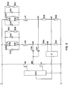
- FIG. 1 illustrates the principle of the circuit arrangement according to the invention using a first embodiment.
- the circuit according to FIG. 1 has a half-bridge inverter consisting of two transistors T10, T11 and fed by a DC voltage source, with a control device ST1.
- An LC output circuit designed as a resonance circuit C11, L1 is connected to the center tap M1 of the half-bridge inverter T10, T11.
- the resonance circuit contains a resonance inductance L1 connected to the center tap M1 and a resonance capacitor C11 which is connected to the resonance inductance L1 and to the positive pole of the DC voltage source.
- the low-pressure discharge lamp LP1 to be operated is integrated into the circuit between the tap A1 and the tap A2, which lies between the resonance inductor L1 and the resonance capacitor C11.
- the electrodes E10, E11 of the low-pressure discharge lamp LP1 are designed as filaments with two electrical connections each.
- the respective first connection of the electrode coils E10, E11 is connected to the tap A1 or to the tap A2, while the second connection of both electrode coils E10, E11 are each led to a connection of the ignition capacitor C12 and the ohmic resistor R11, so that both Ignition capacitor C12 and the resistor R11 are connected in parallel to the discharge path of the low-pressure discharge lamp LP1.
- the circuit arrangement has an ohmic resistor R12, which is connected to the control device ST1 and via a tap A3 to the resonance inductor L1 and the center tap M1.
- the starting voltage required to ignite the low-pressure discharge lamp LP1 and the lamp are provided on the starting capacitor C12 by means of resonance boosting ignited without preheating the lamp electrodes.
- a high-frequency alternating current flows between taps M1 and A1 across the discharge path of the lamp, ie, with a frequency in the range from approximately 20 KHz to approximately 200 KHz.
- the resonant circuit L1, C11 is a closed circuit even when the lamp LP1 is missing, in particular the lamp electrodes are not integrated in the resonant circuit.
- the half-bridge inverter could therefore also be operated if the lamp LP1 is missing or defective.
- the circuit arrangement is equipped with a direct current path, which is formed by the resistor R10, the electrode coil E11, the resistor R11, the electrode coil E10, the resonance inductor L1 and the resistor R12, all of which are connected in series in a direct current manner.
- This path establishes a direct current connection between the positive pole of the direct voltage source and the input of the control device ST1.
- the control device ST1 is supplied with electrical voltage via the direct current path and causes the half-bridge inverter T10, T11 to oscillate.
- the direct current path is interrupted, so that when the circuit arrangement is put into operation again, the control device is not supplied with voltage and the inverter T10, T11 cannot oscillate.
- FIG. 2 shows the application of the invention to two low-pressure discharge lamps LP20, LP21 connected in series in accordance with a second exemplary embodiment.
- the circuit arrangement shown in FIG. 2 has a half-bridge inverter consisting of two field effect transistors T20, T21 and fed by a DC voltage source, which is clocked by a control device ST2.
- An LC output circuit is connected to the center tap M2 of the inverter T20, T21, which is led via the coupling capacitor C20, the resonance inductor L20, the electrode coil E23 of the low-pressure discharge lamp LP21, the resonance capacitor C21 and the electrode coil E20 of the low-pressure discharge lamp LP20 to the positive pole of the DC voltage source.
- the circuit arrangement has the DC path according to the invention, which has the positive pole of the DC voltage source via the electrode coil E20 of the low-pressure discharge lamp LP20, the resistors R21 and R22, the electrode coil E21 of the low-pressure discharge lamp LP20, the secondary winding L21 which is inductively coupled to the resonance inductance L20, and the electrode coil E22 of the low-pressure discharge Connects LP21, the resistors R23 and R24, the electrode filament E23 of the low-pressure discharge lamp LP21, the resonance inductor L20 and via the resistor R20 to the input of the control device ST2.
- the circuit arrangement has a capacitor C23, which is connected on the one hand to the negative pole of the DC voltage source and on the other hand to the resonance inductance and to a connection of the electrode coil E23, and a heating capacitor C22 which, together with the electrode coils E21, E22 and the secondary winding L21, forms a closed circuit forms and enables a preheating of these two lamp electrodes E21, E22 by means of a high-frequency alternating current induced in the secondary winding L21.
- FIG. 3 illustrates the principle of the invention for two low-pressure discharge lamps LP30, LP31 connected in parallel in accordance with a third exemplary embodiment.
- the circuit arrangement shown in FIG. 3 has a half-bridge inverter consisting of two field effect transistors T30, T31 and fed by a DC voltage source, which is controlled by a control device ST3.
- a control device ST3 At the center tap M3 of the inverter T30, T31, two LC output circuits connected in parallel, each for a low-pressure discharge lamp LP30, LP31, are connected.
- the first LC output circuit contains the coupling capacitor C30, the resonance inductor L30 and the parallel-acting resonance capacitors C32, C33.
- the low-pressure discharge lamp LP30 is arranged in parallel with the resonance capacitors C32, C33.
- the second LC output circuit comprises the coupling capacitor C31, the resonance inductor L31 and the parallel-acting resonance capacitors C34, C35.
- the second low-pressure discharge lamp LP31 is arranged in parallel with the resonance capacitors C34, C35.
- the circuit arrangement shown in FIG. 3 has an AND gate U, the output of which is connected to the input of the control device ST3, and two high-resistance direct current paths which are led from the positive pole of the DC voltage source to an input of the AND gate U in each case.
- the electrode filaments E30, the resistors R34 and R35 connected in parallel with the discharge path of the low-pressure discharge lamp LP30, are the electrode filaments E31, the resonance inductor L30 and the resistor R30, which is connected to the tap A4 between the resonance inductor L30 and the coupling capacitor C30, are integrated in series.
- the electrode coil E32, the resistors R36 and R37 arranged parallel to the discharge path of the low-pressure discharge lamp LP31, the electrode coil E33, the resonance inductance L31 and the resistor R32, which is connected to the tap A5 between the resonance inductor L31 and the coupling capacitor C31, are in the second high-resistance direct current path , integrated in series. Furthermore, the circuit arrangement has two further resistors R31, R33, which connect the tap A6 located between the resistor R30 and the AND gate, or the tap A7 arranged between the resistor R32 and the AND gate, to the negative pole of the DC voltage source.
- the two parallel DC paths connected via the AND gate establish a direct current connection between the positive pole of the direct voltage source and the control device ST3 of the inverter T30, T31 and thereby enable the inverter T30 to start , T31 and then lamp operation.
- one of the two direct current paths is interrupted, for example caused by the occurrence of a spiral break in one of the lamp electrodes E30, E31 or E32, E33 integrated in series in this direct current path, the inverter T30, T31 is prevented from oscillating when the supply voltage is switched on again because the DC connection between the positive pole of the DC voltage source and the control device ST3 is then also interrupted.
- the fourth exemplary embodiment of the invention shows the application of the invention to a free-swinging, current-feedback inverter Q40, Q41 for operating a low-pressure discharge lamp LP4 with preheated lamp electrodes E40, E41 designed as filaments.
- This circuit arrangement has two bipolar transistors Q40, Q41 connected as half-bridge inverters and fed by a direct voltage source.
- An LC output circuit is connected to the center tap M4 of the half-bridge inverter Q40, Q41, which contains the primary winding RK4a of a toroidal transformer RK4, a resonance inductor L4 and a resonance capacitor C42, one connection of which is connected to the positive pole of the DC voltage source.
- the circuit arrangement 4 also has two coupling capacitors C40, C41 connected in series with a center tap A8.
- the coupling capacitor C40 is connected via the collector of the bipolar transistor Q40 to the positive pole of the DC voltage source, while the other coupling capacitor C41 is connected to the negative pole of the DC voltage source via the emitter of the second bipolar transistor Q41.
- the low-pressure discharge lamp LP4 is integrated into the circuit arrangement between the center tap A8 and the tap A9, which lies in the LC output circuit between the resonance inductor L4 and the resonance capacitor C42.
- a heating or ignition capacitor C44, C45 are arranged in a first parallel circuit and a series circuit comprising an ohmic resistor R43 and a PTC thermistor KL4 is arranged in a second parallel circuit.
- the two ignition capacitors C44, C45 and the resistance elements R43, KL4 have center taps V1, V2, which are connected to one another.
- the control device for the half-bridge inverter essentially consists of the toroidal transformer RK4, the primary winding RK4a of which is arranged in the LC output circuit, while a secondary winding RK4b or RK4c is connected to the base circuit of the bipolar transistors Q40 or Q41 together with a base series resistor R40 or R41 is.
- the control device has a starting device, which essentially consists of a diac DC4, a capacitor C43 and a diode D4.
- the circuit arrangement of the fourth exemplary embodiment has a high-impedance direct current path, which prevents the half-bridge inverter Q40, Q41 from starting in the event of a defective lamp electrode E40, E41.
- This DC path contains, starting from the positive pole of the DC voltage source, an ohmic resistor R4, the capacitor C43, the center tap M4, the primary winding RK4a, the resonance inductor L4, the electrode coil E40, the ohmic resistor R43, the PTC thermistor KL4, the electrode coil E41, the center tap A8 and an ohmic resistor R42, which is arranged in parallel with the coupling capacitor C41 and connected to the negative pole of the DC voltage source. All of the above-mentioned components of the high-resistance direct current path are connected in series in terms of direct current.
- the capacitor C43 is charged via the direct current path, so that the diac DC4 gives trigger pulses to the base of the bipolar transistor Q40 and thereby triggers the oscillation of the half-bridge inverter Q40, Q41.
- the inverter Q40, Q41 has started up the capacitor C43 is so far discharged via the diode D4 that the diac DC4 does not generate any further trigger pulses for the base of the transistor Q40.
- the half-bridge inverter Q40, Q41 generates a high-frequency alternating current (i.e. with a frequency between approx.
- the PTC thermistor KL4 becomes high-resistance, so that the ignition voltage required for the low-pressure discharge lamp LP4 can be generated with the aid of the now effective ignition capacitor C45 and the LC output circuit designed as a resonance circuit by means of resonance increase.
- FIG. 5 shows a fifth embodiment of the circuit arrangement according to the invention.
- This circuit has a free-swinging, current-feedback, half-bridge inverter Q50, Q51, which is fed by a DC voltage source, for operating a cold-starting, low-pressure discharge lamp LP5, which ignites without preheating the lamp electrodes E50, E51.
- An LC output circuit is connected to the center tap M5 of the half-bridge inverter formed by the bipolar transistors Q50, Q51, starting from the center tap M4 via the primary winding RK5a of a toroidal core transformer, a coupling capacitor C50, a resonance inductor L5 and a resonance capacitor C51 to the collector of the transistor is led to the positive pole of the DC voltage source.
- the low-pressure discharge lamp LP5, a further resonance capacitor C52 and an ohmic resistance element R50 are connected in parallel to the resonance capacitor C51, each in a separate parallel circuit.
- the control device for the half-bridge inverter Q50, Q51 essentially consists of a toroidal transformer RK5, the primary winding RK5a of which is connected to the LC output circuit, and the secondary windings RK5b and RK5c of which are each in a base circuit the switching transistors Q50 and Q51 are integrated, and each of a capacitor C53, C54 and a rectifier diode D50, D51 arranged in parallel thereto, which are also integrated in the base circuit of one of the transistors Q50, Q51.
- the circuit arrangement has a high-impedance direct current path, which connects the base of the bipolar transistor Q51 in a direct current manner to the positive pole of the direct voltage source.
- this high-impedance direct current path comprises the first lamp electrode E50, which is designed as a coil, the ohmic resistance element R50, the second lamp electrode, which is designed as a coil, the resonance inductance L5 and an ohmic resistor R51, which is connected to one between the coupling capacitor C50 and the Resonance inductor L5 located branch point in the LC output circuit and connected to the base of transistor Q51.
- the base of the first transistor Q50 is also connected in direct current form to the positive pole of the direct voltage source via an ohmic resistor R52.
- the base electrode of transistor Q51 does not receive a control signal when the voltage supply is switched on again, thereby preventing the inverter Q50, Q51 from starting up.
- the dimensioning of the electronic components used in the preceding exemplary embodiments depends on the electrical power consumption of the low-pressure discharge lamp to be operated and on the electrical voltage source available.
- FIG. 6 shows a sixth exemplary embodiment of the circuit arrangement according to the invention for operating a compact fluorescent lamp with an electrical power consumption of approximately 23 W on an AC mains voltage of 120 V and 60 Hz.
- This circuit arrangement has a free-swinging, current-feedback half-bridge inverter T60, T61 fed by a direct voltage source.
- An electrolytic capacitor C60 serves as a direct voltage source, which is connected to a mains voltage source via an upstream rectifier GL, a radio interference filter F and a fuse SI.
- An LC output circuit is connected to the center tap M6 of the half-bridge inverter formed by the MOSFET transistors T60, T61 and, starting from the center tap M6, is led via the resonance inductance L6a and the resonance capacitor C61 to the drain connection of the MOSFET transistor T60.
- the coupling capacitor C64 and the fluorescent lamp LP6 are arranged in a parallel circuit to the resonance capacitor C61.
- An ohmic resistor R61 is connected in parallel with the coupling capacitor C64.
- a heating or ignition capacitor C62 or C63 is arranged in a first parallel circuit to the fluorescent lamp LP6.
- a second parallel circuit to the fluorescent lamp LP6 contains a high-ohmic resistor R60 and a PTC thermistor KL6. The center taps V3, V4 between the capacitors C62, C63 and between the resistance elements R60, KL6 are connected to one another.
- the control device for the inverter T60, T61 essentially consists of two secondary windings L6b and L6c, which are inductively coupled to the resonance inductor L6a and are each connected to the gate electrode of a transistor T60 or T61, and one each upstream of the gate electrode Low pass filter R63, C65 or R64, C66.
- the control device has a starting device which comprises the diac DC6, the capacitor C67 and the diode D6. Its circuitry and mode of operation correspond to that of the starting device of the fourth exemplary embodiment.
- the circuit arrangement according to the sixth exemplary embodiment has a high-impedance direct current path which, starting from the positive pole of the electrolytic capacitor C60, the first lamp electrode E60 of the compact fluorescent lamp LP6, the resistor R60, the PTC thermistor KL6, the second lamp electrode E61, the second Resistor R61, the resonance inductor L6 and an ohmic resistor R62, which is connected to a first terminal of the capacitor C67, while the other terminal of the capacitor C67 is led to the negative pole of the electrolytic capacitor C60.
- the inverter T60, T61 After switching on the supply voltage, the inverter T60, T61 is fed from the electrolytic capacitor C60 with the rectified grid voltage.
- the start capacitor C67 is charged via the above-mentioned high-impedance direct current path, so that the diac DC6 gives trigger pulses to the gate of the transistor T61 and thereby triggers the oscillation of the half-bridge inverter T60, T61.
- the start capacitor C67 is discharged via the diode D6 to such an extent that no further trigger pulses are generated by the diac DC6.
- the inverter T60, T61 supplies the LC output circuit as well as the fluorescent lamp LP6 and the parallel circuits to the fluorescent lamp LP6 with a high-frequency AC voltage (between approx. 20 KHz and 200 KHz).
- a high-frequency heating current initially flows through the electrode filaments E60, E61 via the heating capacitor C62 and the PTC thermistor KL6.
- the PTC thermistor KL6 becomes high-resistance, so that the ignition voltage required for the low-pressure discharge lamp LP6 can be generated with the aid of the now effective ignition capacitor C63 and the LC output circuit designed as a resonance circuit by means of resonance increase.
- the amplitude of this direct current is approximately two powers of ten smaller than that of the alternating current generated by the inverter, so that no disturbance of lamp operation by this direct current is to be expected.
- the high-resistance direct current path described above is interrupted, since the electrode filaments E60, E61 are integrated serially in this direct current path, so that when the voltage supply is switched on again, the starting capacitor C67 is not charged and therefore no trigger pulses from the diac DC6 for the Gate of transistor T61 are generated. This prevents the half-bridge inverter T60, T61 from starting up if the lamp electrode E60, E61 is defective.
- the invention is not limited to the exemplary embodiments described in more detail above.
- the DC path according to the invention can also be used in circuit arrangements with other inverters, e.g. B. in full bridge inverters.
Landscapes
- Circuit Arrangements For Discharge Lamps (AREA)
- Medicines That Contain Protein Lipid Enzymes And Other Medicines (AREA)
Applications Claiming Priority (2)
| Application Number | Priority Date | Filing Date | Title |
|---|---|---|---|
| DE4436463 | 1994-10-12 | ||
| DE4436463A DE4436463A1 (de) | 1994-10-12 | 1994-10-12 | Schaltungsanordnung zum Betrieb einer oder mehrerer Niederdruckentladungslampen |
Publications (3)
| Publication Number | Publication Date |
|---|---|
| EP0707437A2 true EP0707437A2 (fr) | 1996-04-17 |
| EP0707437A3 EP0707437A3 (fr) | 1997-12-03 |
| EP0707437B1 EP0707437B1 (fr) | 2001-07-18 |
Family
ID=6530591
Family Applications (1)
| Application Number | Title | Priority Date | Filing Date |
|---|---|---|---|
| EP95115565A Expired - Lifetime EP0707437B1 (fr) | 1994-10-12 | 1995-10-02 | Circuit pour alimenter une ou plusieurs lampes à décharge |
Country Status (5)
| Country | Link |
|---|---|
| EP (1) | EP0707437B1 (fr) |
| JP (1) | JPH08213178A (fr) |
| KR (1) | KR100334378B1 (fr) |
| CA (1) | CA2160309C (fr) |
| DE (2) | DE4436463A1 (fr) |
Cited By (1)
| Publication number | Priority date | Publication date | Assignee | Title |
|---|---|---|---|---|
| EP1945008A1 (fr) * | 2002-02-18 | 2008-07-16 | TridonicAtco GmbH & Co. KG | Capteur de lampes pour un appareil de montage destiné au fonctionnement d'une lampe à décharge |
Families Citing this family (5)
| Publication number | Priority date | Publication date | Assignee | Title |
|---|---|---|---|---|
| DE19819671B4 (de) * | 1998-05-02 | 2008-04-10 | Insta Elektro Gmbh | Schaltungsanordnung zum Schutz von Leuchtstofflampen und elektronischem Vorschaltgerät |
| DE19916080C2 (de) * | 1999-04-09 | 2001-11-22 | Vossloh Schwabe Elektronik | Vorschaltgerät mit Fehlererkennung |
| DE10200022A1 (de) | 2002-01-02 | 2003-07-17 | Philips Intellectual Property | Schaltungsanordnung zum Betrieb einer oder mehrerer Lampen |
| KR100625262B1 (ko) | 2004-04-14 | 2006-09-20 | 조당 | 개선된 공진출력 회로를 갖는 고압방전 형광등용 전자식안정기 |
| KR100686471B1 (ko) * | 2005-10-11 | 2007-02-26 | 주식회사 화승전기 | 향상된 효율 및 개선된 출력특성을 갖는 전자식 안정기 |
Citations (1)
| Publication number | Priority date | Publication date | Assignee | Title |
|---|---|---|---|---|
| DE4303595A1 (de) | 1993-02-08 | 1994-08-11 | Patent Treuhand Ges Fuer Elektrische Gluehlampen Mbh | Schaltungsanordnung zum Betrieb einer Leuchtstofflampe |
Family Cites Families (3)
| Publication number | Priority date | Publication date | Assignee | Title |
|---|---|---|---|---|
| US3869640A (en) * | 1973-07-09 | 1975-03-04 | Taras Avenir Kolomyjec | Power supply arrangement for fluorescent tubes, thermionic devices and the like |
| DE3805510A1 (de) * | 1988-02-22 | 1989-08-31 | Patent Treuhand Ges Fuer Elektrische Gluehlampen Mbh | Schaltungsanordnung zum betrieb einer niederdruckentladungslampe |
| US5220247A (en) * | 1992-03-31 | 1993-06-15 | Moisin Mihail S | Circuit for driving a gas discharge lamp load |
-
1994
- 1994-10-12 DE DE4436463A patent/DE4436463A1/de not_active Withdrawn
-
1995
- 1995-10-02 EP EP95115565A patent/EP0707437B1/fr not_active Expired - Lifetime
- 1995-10-02 DE DE59509422T patent/DE59509422D1/de not_active Expired - Fee Related
- 1995-10-09 JP JP7288005A patent/JPH08213178A/ja active Pending
- 1995-10-11 CA CA002160309A patent/CA2160309C/fr not_active Expired - Fee Related
- 1995-10-12 KR KR1019950035028A patent/KR100334378B1/ko not_active Expired - Fee Related
Patent Citations (1)
| Publication number | Priority date | Publication date | Assignee | Title |
|---|---|---|---|---|
| DE4303595A1 (de) | 1993-02-08 | 1994-08-11 | Patent Treuhand Ges Fuer Elektrische Gluehlampen Mbh | Schaltungsanordnung zum Betrieb einer Leuchtstofflampe |
Cited By (1)
| Publication number | Priority date | Publication date | Assignee | Title |
|---|---|---|---|---|
| EP1945008A1 (fr) * | 2002-02-18 | 2008-07-16 | TridonicAtco GmbH & Co. KG | Capteur de lampes pour un appareil de montage destiné au fonctionnement d'une lampe à décharge |
Also Published As
| Publication number | Publication date |
|---|---|
| KR960016646A (ko) | 1996-05-22 |
| JPH08213178A (ja) | 1996-08-20 |
| EP0707437A3 (fr) | 1997-12-03 |
| EP0707437B1 (fr) | 2001-07-18 |
| DE59509422D1 (de) | 2001-08-23 |
| CA2160309A1 (fr) | 1996-04-13 |
| DE4436463A1 (de) | 1996-04-18 |
| CA2160309C (fr) | 2004-12-07 |
| KR100334378B1 (ko) | 2002-10-31 |
Similar Documents
| Publication | Publication Date | Title |
|---|---|---|
| EP0616752B1 (fr) | Circuit pour actionner une ou plusieurs lampe(s) a decharge a basse pression | |
| EP0239793B1 (fr) | Disposition de circuit pour la mise en oeuvre de lampes à décharge basse pression | |
| EP0707438B1 (fr) | Ballast pour au moins une lampe à décharge | |
| DE2941822A1 (de) | Vorschaltanordnung zum betreiben von niederdruckentladungslampen | |
| EP0185179A1 (fr) | Circuit d'allumage pour une lampe à décharge à basse pression | |
| EP0798952A1 (fr) | Circuit pour l'opération de lampes électriques et procédé d'opération | |
| DE2710036A1 (de) | Abgestimmter vorschaltschwingkreis | |
| EP0378992B1 (fr) | Circuit de commande de lampes à décharge | |
| EP0800335A2 (fr) | Circuit pour alimenter des lampes électriques | |
| EP0693864B1 (fr) | Circuit pour alimenter une ou plusieurs lampes à décharge basse-pression | |
| EP0707437B1 (fr) | Circuit pour alimenter une ou plusieurs lampes à décharge | |
| DE69709604T2 (de) | Schaltungsanordnung | |
| DE4005776C2 (de) | Schaltungsanordnung zum Starten und zum Betrieb einer Gasentladungslampe | |
| EP1289350B1 (fr) | Circuit de commande pour lampe à décharge avec électrodes préchauffées | |
| EP0648068B1 (fr) | Circuit d'alimentation de lampes électriques | |
| DE3504803A1 (de) | Gegentaktgenerator | |
| EP1477046B1 (fr) | Capteur de lampe pour ballast concu pour faire fonctionner une lampe a decharge gazeuse | |
| EP1424880A2 (fr) | Appareil pour alimenter des lampes à décharge | |
| EP2103192B1 (fr) | Montage électrique et procédé pour allumer et faire fonctionner une ou plusieurs lampes à décharge | |
| EP1223792B1 (fr) | Circuit d'amorçage des lampes électriques | |
| EP1962565B1 (fr) | Ballast doté d'une commutation de puissance | |
| DD264564B5 (de) | Schaltungsanordnung fuer die zuendung und den betrieb einer niederdruckentladungslampe | |
| DE4412458A1 (de) | Schaltungsanordnung zum Betrieb von Entladungslampen | |
| DE10204432A1 (de) | Elektronisches Vorschaltgerät mit Wendelheizung | |
| EP0563770A1 (fr) | Ballast electronique |
Legal Events
| Date | Code | Title | Description |
|---|---|---|---|
| PUAI | Public reference made under article 153(3) epc to a published international application that has entered the european phase |
Free format text: ORIGINAL CODE: 0009012 |
|
| AK | Designated contracting states |
Kind code of ref document: A2 Designated state(s): BE DE FR GB IT NL |
|
| PUAL | Search report despatched |
Free format text: ORIGINAL CODE: 0009013 |
|
| AK | Designated contracting states |
Kind code of ref document: A3 Designated state(s): BE DE FR GB IT NL |
|
| 17P | Request for examination filed |
Effective date: 19980107 |
|
| GRAG | Despatch of communication of intention to grant |
Free format text: ORIGINAL CODE: EPIDOS AGRA |
|
| 17Q | First examination report despatched |
Effective date: 20001103 |
|
| GRAG | Despatch of communication of intention to grant |
Free format text: ORIGINAL CODE: EPIDOS AGRA |
|
| GRAH | Despatch of communication of intention to grant a patent |
Free format text: ORIGINAL CODE: EPIDOS IGRA |
|
| GRAH | Despatch of communication of intention to grant a patent |
Free format text: ORIGINAL CODE: EPIDOS IGRA |
|
| GRAA | (expected) grant |
Free format text: ORIGINAL CODE: 0009210 |
|
| AK | Designated contracting states |
Kind code of ref document: B1 Designated state(s): BE DE FR GB IT NL |
|
| RIC1 | Information provided on ipc code assigned before grant |
Free format text: 7H 05B 41/292 A |
|
| REF | Corresponds to: |
Ref document number: 59509422 Country of ref document: DE Date of ref document: 20010823 |
|
| ITF | It: translation for a ep patent filed | ||
| GBT | Gb: translation of ep patent filed (gb section 77(6)(a)/1977) |
Effective date: 20010925 |
|
| ET | Fr: translation filed | ||
| REG | Reference to a national code |
Ref country code: GB Ref legal event code: IF02 |
|
| PLBE | No opposition filed within time limit |
Free format text: ORIGINAL CODE: 0009261 |
|
| STAA | Information on the status of an ep patent application or granted ep patent |
Free format text: STATUS: NO OPPOSITION FILED WITHIN TIME LIMIT |
|
| 26N | No opposition filed | ||
| PGFP | Annual fee paid to national office [announced via postgrant information from national office to epo] |
Ref country code: GB Payment date: 20021010 Year of fee payment: 8 |
|
| PGFP | Annual fee paid to national office [announced via postgrant information from national office to epo] |
Ref country code: NL Payment date: 20021021 Year of fee payment: 8 Ref country code: BE Payment date: 20021021 Year of fee payment: 8 |
|
| PGFP | Annual fee paid to national office [announced via postgrant information from national office to epo] |
Ref country code: FR Payment date: 20021023 Year of fee payment: 8 |
|
| PG25 | Lapsed in a contracting state [announced via postgrant information from national office to epo] |
Ref country code: GB Free format text: LAPSE BECAUSE OF NON-PAYMENT OF DUE FEES Effective date: 20031002 |
|
| PG25 | Lapsed in a contracting state [announced via postgrant information from national office to epo] |
Ref country code: BE Free format text: LAPSE BECAUSE OF NON-PAYMENT OF DUE FEES Effective date: 20031031 |
|
| BERE | Be: lapsed |
Owner name: *PATENT-TREUHAND-G.- FUR ELEKTRISCHE GLUHLAMPEN M. Effective date: 20031031 |
|
| PG25 | Lapsed in a contracting state [announced via postgrant information from national office to epo] |
Ref country code: NL Free format text: LAPSE BECAUSE OF NON-PAYMENT OF DUE FEES Effective date: 20040501 |
|
| GBPC | Gb: european patent ceased through non-payment of renewal fee |
Effective date: 20031002 |
|
| PG25 | Lapsed in a contracting state [announced via postgrant information from national office to epo] |
Ref country code: FR Free format text: LAPSE BECAUSE OF NON-PAYMENT OF DUE FEES Effective date: 20040630 |
|
| NLV4 | Nl: lapsed or anulled due to non-payment of the annual fee |
Effective date: 20040501 |
|
| REG | Reference to a national code |
Ref country code: FR Ref legal event code: ST |
|
| PGFP | Annual fee paid to national office [announced via postgrant information from national office to epo] |
Ref country code: DE Payment date: 20051219 Year of fee payment: 11 |
|
| PGFP | Annual fee paid to national office [announced via postgrant information from national office to epo] |
Ref country code: IT Payment date: 20061031 Year of fee payment: 12 |
|
| PG25 | Lapsed in a contracting state [announced via postgrant information from national office to epo] |
Ref country code: DE Free format text: LAPSE BECAUSE OF NON-PAYMENT OF DUE FEES Effective date: 20070501 |
|
| PG25 | Lapsed in a contracting state [announced via postgrant information from national office to epo] |
Ref country code: IT Free format text: LAPSE BECAUSE OF NON-PAYMENT OF DUE FEES Effective date: 20071002 |