EP0708492B1 - Mikrostreifenleitungsantenne insbesondere für Uhrenanwendung - Google Patents
Mikrostreifenleitungsantenne insbesondere für Uhrenanwendung Download PDFInfo
- Publication number
- EP0708492B1 EP0708492B1 EP95116148A EP95116148A EP0708492B1 EP 0708492 B1 EP0708492 B1 EP 0708492B1 EP 95116148 A EP95116148 A EP 95116148A EP 95116148 A EP95116148 A EP 95116148A EP 0708492 B1 EP0708492 B1 EP 0708492B1
- Authority
- EP
- European Patent Office
- Prior art keywords
- conductive element
- antenna
- frequency adjustment
- center
- adjustment plate
- Prior art date
- Legal status (The legal status is an assumption and is not a legal conclusion. Google has not performed a legal analysis and makes no representation as to the accuracy of the status listed.)
- Expired - Lifetime
Links
- 239000000758 substrate Substances 0.000 claims description 46
- 239000004020 conductor Substances 0.000 claims description 23
- 230000005284 excitation Effects 0.000 claims description 17
- 239000002184 metal Substances 0.000 claims description 4
- 229910052751 metal Inorganic materials 0.000 claims description 4
- 239000004033 plastic Substances 0.000 claims description 3
- 230000010287 polarization Effects 0.000 description 21
- 239000000463 material Substances 0.000 description 8
- 230000000694 effects Effects 0.000 description 7
- 238000004519 manufacturing process Methods 0.000 description 7
- 239000004593 Epoxy Substances 0.000 description 6
- 125000006850 spacer group Chemical group 0.000 description 6
- 239000000919 ceramic Substances 0.000 description 3
- 238000013461 design Methods 0.000 description 3
- 238000000034 method Methods 0.000 description 3
- 238000013459 approach Methods 0.000 description 2
- 238000005388 cross polarization Methods 0.000 description 2
- 238000010586 diagram Methods 0.000 description 2
- 230000005855 radiation Effects 0.000 description 2
- RYGMFSIKBFXOCR-UHFFFAOYSA-N Copper Chemical compound [Cu] RYGMFSIKBFXOCR-UHFFFAOYSA-N 0.000 description 1
- 229920006362 Teflon® Polymers 0.000 description 1
- 230000009286 beneficial effect Effects 0.000 description 1
- 230000005540 biological transmission Effects 0.000 description 1
- 238000010276 construction Methods 0.000 description 1
- 229910052802 copper Inorganic materials 0.000 description 1
- 239000010949 copper Substances 0.000 description 1
- 230000001066 destructive effect Effects 0.000 description 1
- 238000005421 electrostatic potential Methods 0.000 description 1
- 238000005516 engineering process Methods 0.000 description 1
- 238000005530 etching Methods 0.000 description 1
- 239000011521 glass Substances 0.000 description 1
- 239000011810 insulating material Substances 0.000 description 1
- 238000009413 insulation Methods 0.000 description 1
- 239000007769 metal material Substances 0.000 description 1
- 238000000926 separation method Methods 0.000 description 1
- 230000008054 signal transmission Effects 0.000 description 1
- 239000000126 substance Substances 0.000 description 1
Images



Classifications
-
- H—ELECTRICITY
- H01—ELECTRIC ELEMENTS
- H01Q—ANTENNAS, i.e. RADIO AERIALS
- H01Q1/00—Details of, or arrangements associated with, antennas
- H01Q1/27—Adaptation for use in or on movable bodies
- H01Q1/273—Adaptation for carrying or wearing by persons or animals
-
- H—ELECTRICITY
- H01—ELECTRIC ELEMENTS
- H01Q—ANTENNAS, i.e. RADIO AERIALS
- H01Q9/00—Electrically-short antennas having dimensions not more than twice the operating wavelength and consisting of conductive active radiating elements
- H01Q9/04—Resonant antennas
- H01Q9/0407—Substantially flat resonant element parallel to ground plane, e.g. patch antenna
Definitions
- the present invention relates to antennas intended for convert an alternating voltage into a microwave and vice versa and, more particularly, to antennas of this type comprising a separate conductive element and a ground plane by a dielectric substrate. These antennas are also known under the English name "microstrip patch antennas".
- the invention can be used to transmit and / or receive GPS signals ("Global Positioning System"), and, moreover, it can be incorporated into watches or other products watchmakers. The invention will therefore be described in the context of this application example. However, it will be understood that the invention is of course not limited to this application.
- the miniaturization of the antennas of the type described above is usually accomplished by using a substrate of a very high permittivity. This invariably involves the use of a ceramic substrate. The costs of manufacture of such a substrate are often high.
- a miniaturized antenna is known from the patent application EP-A-0 525 726.
- This document describes a polarized antenna circular comprising a dielectric substrate having two opposite sides. On one side is fixed a ground plane and on the other side is fixed a conductive element.
- This element conductor is provided with an electrical excitation point off-center with respect to the axis of rotation of the antenna. It is also provided with slots placed at its periphery and passing virtually through its center. The characteristics of these slots, such as their length or positioning at the periphery of the conductive element, used to determine the resonant frequency of the antenna.
- Another antenna of this type is also known from the publication IEEE Transactions on vehicular technology, vol.40, no.2, May 1991, New York US pages 483-486, entitled "A flat energy density antenna system for mobile telephone ”.
- This publication also describes the use of slots allowing in particular to increase the resonant frequency of the antenna by reducing the effective radius of the element conductor, i.e. by reducing the length of the slots used.
- Miniature antennas of this type have a width very narrow band. Therefore, under tolerances manufacturing, design and construction of these antennas is a difficult task.
- the mechanical adjustment of edges of the conductive element is a technique used long time to get the resonant frequency of the desired antenna.
- such a solution is both destructive and cumbersome.
- the object of the present invention is to provide an antenna miniaturized of the type defined above which remedies everything less in part to the disadvantages of state antennas prior art.
- Another object of the invention is to provide an antenna miniaturized of the type defined above which is compact, and which is relatively easy and inexpensive to manufacture.
- an object of the invention is to provide a miniaturized antenna of the type defined above which allows a simple adjustment of its resonant frequency.
- Another object of the invention is to provide an antenna miniaturized of the type defined above which is capable of being used in a watch.
- the invention therefore relates to an antenna intended to convert an alternating voltage, coming from a antenna circuit, in a wave with linear polarization and vice versa, the characteristics of which are set out in claim 1.
- the invention also relates to an antenna intended for convert alternating voltage from a circuit antenna, in a wave with linear or circular polarization and vice versa, the characteristics of which are set out in claim 8.
- the invention allows the creation of a miniaturized antenna without requiring the use of a very high permittivity substrate.
- the antenna comprises an adjustment plate frequency, mounted on the center of the conductive element and on an axis perpendicular to the plane of the conductive element, the distance between the periphery and the center of the plate, the along the axis where the slots extend, being variable by so that, by rotation, the adjustment plate frequency acts to modify the effective length of the slots.
- the rotation of the plate frequency adjustment around its axis allows, an adjustment simple and precise antenna resonant frequency, and this over a bandwidth greater than the width of conductive element strip.
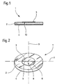
- the arrangement of the miniaturized antenna 1 according to the invention shown in Figures 1 and 2 includes a dielectric substrate 2, a conductive element 3 and a ground plane 4.
- the conductive element 3 has the form general of a disc and according to the Anglo-Saxon denomination is called "radiating patch".
- the conductive element 3 and the ground plane 4 are deposited on surfaces opposite of the dielectric substrate 2.
- the antenna 1 has a geometry suitable for receiving and emitting waves at linear polarization.
- the conductive element 3 has slots 5 and 6 diametrically opposite and aligned along the axis 7. These slots 5 and 6 extend from the periphery towards the center of the conductive element 3.
- An excitation point 8 is located in the plane of the conductive element 3, on a axis 9 which is perpendicular to axis 7. The excitation is ensured by means of a coaxial cable whose conductor central 10 passes through the substrate 2 and is welded to the element conductor 3 at the point of excitation 8.
- FIG. 3 shows more precisely the geometry of the conductive element 3. It can be seen that the slots 5 and 6 both have a length r x and that the conductive element 3 has a diameter 2R, R being the radius of the latter.
- the slots 5 and 6 constitute a capacitive load for the antenna 1.
- Theoretical considerations which will not be repeated here since they go beyond the scope of the present patent application, show that the resonance frequency of the antenna 1 strongly depends of the length r x of the slots 5 and 6. According to these considerations, when r x is zero, the antenna 1 resonates at a frequency f c . However, when the value of r x approaches R, the resonant frequency approaches f c / 2.
- the diameter 2R of the antenna is a function of the inverse of the resonance frequency f c thereof.
- the resonance frequency f c is close to f c / 2 for a certain dimension 2R, one can also choose to reduce the dimension 2R by half for a certain resonance frequency f c . That is to say, the maximum dimension of the antenna 1 can be reduced by a factor of 2 when the slots extend substantially over the entire distance separating the periphery from the center of said conductive element.
- the slots 5 and 6 can be produced by cutting the conductive element 3 by means of a laser beam. Of course, the slots 5 and 6 can also be produced by etching or any other chemical or mechanical treatment of the conductive element 3.
- the circular shape of the element conductor 3 of figures 2 and 3 represents only one example of a form of the conductive element of the invention.
- a square shape can also be used, as well as any other conductive element which is delimited at its periphery by an edge which gives this element a double planar symmetry along two axes perpendicular.
- the excitation point is on one of the two axes of symmetry of the conductive element and the slots 5 and 6 extend on the other axis of symmetry.
- Figure 4 shows the geometry of an element conductor 20 capable of receiving and transmitting both circularly polarized signals as signals to linear polarization.
- the conductive element 20 comprises slots 21 and 22 which extend from its periphery towards the center and which are aligned on the same axis 23.
- the conductive element 20 includes slots 24 and 25 which extend from its periphery towards the center and which are aligned on the same axis 26 perpendicular to the axis 23.
- An excitation point 27 is located on an axis 45 ° offset from the two axes 23 and 24.
- the lengths r x of the slots 21 and 22 and r y of the slots 24 and 25 must be equal.
- a right circular polarization is obtained if, for an excitation point 27 as described above, r x is greater than r y according to a suitable choice.
- the circular shape of the conductive element 20 of FIG. 4 only represents a particular shape of the conductive element of the invention. It goes without saying that a square shape can also be used or any other form of conductive element delimited at its periphery by an edge which gives it a double planar symmetry along two perpendicular axes.
- the excitation point 27 of the conductive element is on a bisecting axis of the angle formed between the two axes of symmetry.
- the pairs of slots 21, 22 and 23, 24 extend respectively on the two axes of symmetry.
- the resonant frequency of the antenna according to the invention varies as a function of the distance r, if we consider the conductive element 3 of FIG. 3, or as a function of the distances r x and r y , if we consider the conductive element shown in FIG. 4.
- r the distance between the conductive elements 3 of FIG. 3
- r x and r y the distance between the conductive elements shown in FIG. 4.
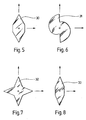
- Figures 5, 6, 7 and 8 show respectively examples 30, 31, 32 and 33 of geometries of such a plate frequency adjustment, the distance between the periphery and the center of said plate, along at least one of axes defined by the slots of the conductive element, varying according to the angle of rotation of the plate about an axis perpendicular A to the plane of the plate and passing through the center of the plate relative to the element driver.
- the structures shown in Figures 5 to 8 can be done in several ways. For example, they can be printed on a dielectric substrate or machined from a metal block. Several forms of plates are possible and the choice of these depends on the necessary tuning range as well as the finesse of the agreement.
- Figures 9 and 10 show an antenna 40 comprising a dielectric substrate 41, a ground plane 42, a conductive element 43 and an adjustment plate frequency 44, the latter being separated from the element conductor 43 by another dielectric substrate 45.
- the conductive element 43 has orthogonal slots 46, 47, 48 and 49.
- the rotation of the adjustment plate frequency 44 around axis A with respect to the element conductor 43 changes the effective lengths of the slots 46 to 49 and, therefore, changes the frequency of antenna resonance 40.
- the antenna 40 also comprises a coaxial connector whose central conductor 50 passes through the substrate 41.
- the central conductor. 50 is welded to the element conductor 43, while the outer conductor is soldered to ground plane 42.
- the two conductors of the connector coaxial are also connected to an antenna circuit.
- the antenna 40 converts an alternating voltage from of the antenna circuit, between the two conductors of the coaxial connector, into a microwave and vice versa.
- the antenna 40 has a central support 51 which passes through openings 52, 53 and 54 in the center of the structure shown in Figure 9 and which maintains the alignment of the various elements of the antenna 40.
- the central support 51 can be realized either in material insulating or conductive material, the difference related to the use of one or the other of these two materials being a small change in the resonant frequency. This difference can be offset anyway by a rotation of the frequency adjustment plate 44.
- the center of the conductive element 43 is a point of zero tension and that the fact that this point either in open circuit or in short circuit with ground does not affect the characteristics of the antenna.
- the conductive element 20 is linearly polarized along a line passing through the center of the conductive element 20 and by the excitation point 27.
- this linear polarization can be adjusted.
- adjusting the resonant frequency of an antenna is only required for overcome the uncertainty of the value of the permittivity of the substrate.
- the antenna can be adjusted by using the disturbance segments that come to be described.
- Frequency adjustment plates simple narrow band can be used so that the antenna can be tuned to a desired frequency.
- Figures 13, 14 and 15 show examples of shape plates 70, 71 and 72.
- Figure 16 shows the arrangement of the frequency adjustment plate 70 of FIG. 13 and of the conductive element 65 of FIG. 12.
- FIG. 17 shows the arrangement of the frequency adjustment plate 72 of FIG. 15 and of the conductive element 64 of the figure 11. Note that the shape and size of the frequency adjustment plates 70, 71 and 72 relative to to the corresponding conductive elements are such that the distance between the periphery and the center of the plates 70, 71 and 72 vary little depending on the angle of rotation.
- FIGS. 7 and 8 show an example of such a combination of plates.
- the frequency adjustment plates 32 and 33 are supported above the conductive element 20 of FIG. 4.
- the adjustment plate can first be rotated 32 to establish linear polarization at a desired frequency.
- the frequency adjustment plate 33 can be rotated to introduce a controlled offset between the dimensions r x and r y , which leads the antenna to circular polarization operation.
- the use of two frequency adjustment plates makes it possible to be able to provide wider manufacturing tolerances for the antenna.
- a conductive element having the shape shown in FIG. 3 is etched from a substrate made of a material sold under the trade designation ULTRALAM®.
- the initial dimensions of the substrate were 144 x 1.5 mm 3 and its relative permittivity is 2.5.
- a circular hole with a diameter of 1 mm is drilled in the center of the substrate.
- the antenna is energized by means of a signal applied to the conductive element 3 via a standard 50 ⁇ SMA coaxial cable.
- a hole with a diameter equal to 3 ⁇ is formed in the center of the conductive element.
- a frequency adjustment plate was used having the shape shown in Figure 5.
- the arrangement of the antenna is represented in figure 19.
- the plate of frequency setting is burned from a disc circular in epoxy. We chose this material in this case due to its great rigidity.
- the circular disc has a thickness of 0.8 mm and a diameter of 60 mm.
- another epoxy disc such as that referenced 45 in Figure 9. This disc serves as a plate spacing between the conductive element and the plate frequency setting.
- the spacer plate has a thickness of 0.1 mm and a diameter of 25 mm.
- the angle of rotation of the plate frequency adjustment 33 of the antenna shown in the figure 19 is limited to a value of 90 °.
- the use of the frequency adjustment plate shown in Figure 6 allows rotation by an angle 180 ° and therefore a finer adjustment of the frequency in the same frequency range.
- An antenna was made having an arrangement such as that shown in FIG. 18. This antenna was excited at a single point situated on an axis bisecting the angle formed between the two orthogonal axes of the slots of the conductive element.
- this excitation technique is quite sensitive compared to other known techniques and that it requires a precise separation between the two degenerate modes of the antenna.
- the geometry of the conductive element shown in Figure 4 can be adapted for this purpose using an asymmetrical frequency adjustment structure.
- a circularly polarized excitation requires asymmetry in the dimensions of the slots of the conductive element.
- the fact that the length r x is greater than the length r y leads to circular polarization to the right.
- the conductive element is etched from a substrate made of a material sold under the trade designation ULTRALAM®.
- the initial dimensions of the substrate were 144 x 144 x 1.5 mm 3 and its relative permittivity is 2.5.
- a circular hole with a diameter of 1 mm is drilled in the center of the substrate.
- the antenna is energized by means of a signal applied to the conductive element 3 via a standard 50 ⁇ SMA coaxial cable.
- a hole with a diameter equal to 3 ⁇ is provided in the center of the conductive element.
- Frequency adjusting plates having the form shown in Figures 7 and 8 are used.
- the antenna layout is shown in Figure 18.
- the frequency adjustment plate of figure 7 is engraved from a circular epoxy disc.
- the disc circular has a thickness of 0.1 mm and a diameter of 60 mm.
- the frequency adjustment plate of figure 8 is also engraved from a circular disc in epoxy.
- the circular disc has a thickness of 0.8 mm and a diameter of 50 mm.
- Another epoxy disc like that designated by the reference numeral 45 in FIG. 9, is used as a spacer plate and is arranged between the conductive element and the frequency adjustment plate.
- the spacer plate has a thickness of 0.1 mm and a 25 mm diameter. No spacer disc is used between the two frequency adjustment plates.
- the range of adjustment of the resonant frequency of the antenna is slightly lower than the adjustment range from the previous example due to the lag between two degenerate modes of the antenna in the second example. This variation is around 10%.
- the report standing waves in tension, measured at resonance, is better than 2 at a frequency of 2.306 MHz.
- a conductive element having the shape shown in FIG. 11 is etched from a substrate made of a material sold under the trade name TMM-10®, this conductive element comprising disturbance segments allowing operation with circular polarization to the right.
- the substrate is circular and has a diameter of 34.5 mm.
- the thickness of the substrate is 0.635 mm and its relative permittivity is 9.2.
- a circular hole with a diameter of 1.4 mm is drilled in the center of the substrate.
- the antenna is energized by means of a signal applied to the conductive element via a standard 50 ⁇ SMA coaxial cable.
- a frequency adjustment plate was used having the shape shown in Figure 15.
- the arrangement of the antenna is represented in figure 17.
- the plate of frequency setting is burned from a disc circular in epoxy. This material is preferred here in because of its great rigidity.
- the circular disc has a 0.8 mm thick and 25 mm in diameter.
- a disk TEFLON® dielectric is used as a plate and is arranged between the conductive element and the frequency adjustment plate.
- the spacer plate has a thickness of 0.254 mm and a diameter of 25 mm. This structure provides a range of adjustment frequency of the order of 2%.
- the antenna is adjusted to the frequency of GPS signals (1.57542 GHz) by the rotation of the adjustment plate frequency.
- the measured axial ratio is 2.54 dB and the bandwidth, with a standing wave ratio in voltage equal to 2, is 12 MHz.
- the gain measured is -6 dBi.
- Example 4 Circular polarization and band adjustment narrow.
- This example uses a conductive element comprising disturbance segments for operation with right-hand circular polarization.
- a conductive element having the shape shown in FIG. 12 is etched from a TMM-10® substrate.
- the substrate is circular and has a diameter of 34.5 mm.
- the thickness of the substrate is 1.27 mm and its relative permittivity is 9.2.
- a circular hole with a diameter of 1.4 mm is drilled in the center of the substrate.
- the antenna is energized by means of a signal applied to the conductive element via a standard 50 ⁇ SMA coaxial cable.
- a hole with a diameter equal to 1.631 mm is drilled in the center of the conductive element.
- a frequency adjustment plate having the form shown in figure 13 is machined from a block of copper. No spacer disc is used, but an air gap is created by supporting the adjustment plate frequency 0.2 mm above the conductive element at by means of a central support element.
- the layout of the antenna is illustrated in Figure 16.
- the plate geometry frequency setting 70 is such that the distance between its periphery and its origin varies linearly between 4.5 mm and 8.75 mm depending on the angle of rotation thereof.
- the antenna in this example is mounted in a housing plastic and is set to the frequency of GPS signals (1.57542 GHz) by rotation of the adjustment plate frequency.
- the measured axial ratio, with the housing fixed at the antenna ground plane, is 1.78 dB and the bandwidth when the standing wave ratio in voltage is equal to 2 is 11 MHz.
- the gain measured is -4.0 dB.
- the frequency adjustment plate 70 can be replaced by the frequency adjustment plate 71 of FIG. 14.
- This frequency adjustment plate is easier to manufacture because it can be made from bars currently available in the trade.
- the adjustment range in this case is around 3% and the maximum angle of rotation is 45 °.
- the geometry of the element conductor allows proper size control. of the current shapes such as circular shapes or rectangular have a fixed size according to the frequency of desired resonance and according to the characteristics of the substrate used. Using a slot length variable, you can modify the antenna dimensions by a factor of 2. Furthermore, the shape of the conductive element allows optimal use of the available space, because there is little unmetallized surface. Consequently, the invention allows miniaturization of the antenna while keeping an optimal gain / size ratio.
- Examples 3 and 4 above describe antennas which are intended to receive, waves of GPS signals transmitted by satellite.
- the dimensions of the antenna are as it can be mounted in a watch case.
- the antenna can for example be arranged between the engine and the needles.
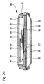
- FIG 20 is a sectional view of a watch 80 comprising a box 81, a bottom 82 and a glass 83.
- the watch 80 has a dielectric substrate 85, a plane of earth 86 connected to the box 81, a conductive element 87 and a frequency adjustment plate 88, the latter being separated from the conductive element 87 by another dielectric substrate 89.
- the conductive element comprises two pairs of orthogonal slots. The length of one of pairs of slots is greater than the length of the other pair, to ensure circular polarization antenna 87.
- the rotation of an adjustment plate frequency 88 with respect to the conductive element 87 modifies the lengths of the two pairs of orthogonal slots and, therefore, changes the resonant frequency of antenna 84.
- Watch 80 also includes a coaxial cable 90 whose central conductor crosses the substrate dielectric 85. This central conductor is soldered to the conductive element 87, while the external conductor is soldered to ground plane 86. The two conductors of the coaxial cable are also connected to an antenna circuit 91, arranged in watch 80, between the back 82 and the plane mass 86.
- watch 80 has a central support 92 on which the hour and minute hands are mounted and seconds, respectively 93, 94 and 95.
- the support central 92 is connected to a watch movement 96 which is also arranged between the bottom 82 and the ground plane 86.
- the watch movement 96 turns the hands 93 to 95 of watch 80 via the central support 92 to indicate the standard time.
- the central support 92 serves to maintain the alignment various elements 85 to 88 of the antenna 80.
- the environment close to antenna 80 has a certain effect on the resonant frequency of the antenna.
- the angular positions of the needles 93 to 95 by compared to the slots of the conductive member 87 have a some effect on the resonant frequency of the antenna.
- the hands 93 to 95 are brought by the watch movement 96 in angular positions that have little influence on the resonant frequency of the antenna 80.
- these angular positions are such that none of the needles 93 to 95 are superimposed on the slots of the conductive member 87.
- the needles 93 to 95 can be brought in the same positions angular during each reception / transmission, so that the influence of needles 93 to 95 on the frequency of resonance of antenna 80 is always the same.
- the frequency adjustment structures of resonance of the antenna which have just been described, allow on the one hand, compensation for the non homogeneity of the characteristics of the substrate material, and, on the other hand, a frequency adjustment on a band large.
- the dimensions of the antenna remain minimum because the frequency adjustment structures only slightly increase the thickness of the antenna.
Landscapes
- Waveguide Aerials (AREA)
- Variable-Direction Aerials And Aerial Arrays (AREA)
- Transceivers (AREA)
- Support Of Aerials (AREA)
Claims (19)
- Antenne, die dazu bestimmt ist, eine von einer Antennenschaltung stammende Wechselspannung in eine Mikrowelle mit linearer Polarisation und umgekehrt umzusetzen, und umfaßt:wobei das Leiterelement einen. Erregungspunkt (8) aufweist, über den es mit der Antennenschaltung verbunden ist, wobei diese letztere die Wechselspannung zwischen dem Erregungspunkt und der Masseebene anlegt;ein erstes dielektrisches Substrat (2; 41), das zwei gegenüberliegende Seiten aufweist;ein Leiterelement (3), das an einer ersten Seite des ersten dielektrischen Substrats befestigt ist und an seinem Umfang durch einen Rand begrenzt ist, der diesem Element eine doppelte planare Symmetrie längs zweier senkrechter Achsen (7, 9) verleiht; undeine Masseebene (4; 42), die an der zweiten Seite des ersten dielektrischen Substrats befestigt ist;
wobei sich der Erregungspunkt (8) auf einer ersten (9) der Achsen (7, 9) befindet;
wobei das Leiterelement (3) außerdem umfaßt:wobei die Antenne dadurch gekennzeichnet ist, daß sie außerdem umfaßt:ein erstes Paar Schlitze (5, 6), die sich auf der zweiten (7) der Achsen (7, 9) vom Umfang zur Mitte des Leiterelements im wesentlichen über den gesamten Abstand, der den Umfang von der Mitte des Leiterelements trennt, erstrecken;eine erste Frequenzeinstellplatte (30; 31; 32; 33; 44; 70; 71; 72), die an der Mitte des Leiterelements und an einer Achse senkrecht zur Ebene des Leiterelements angebracht ist, wobei der Abstand zwischen dem Umfang und der Mitte der ersten Platte längs der zweiten Achse derart veränderlich ist, daß durch Drehung die erste Frequenzeinstellplatte in der Weise wirkt, daß die effektive Länge der Schlitze (5, 6) verändert wird. - Antenne nach Anspruch 1, dadurch gekennzeichnet, daß die Frequenzeinstellplatte aus einem Metallblock maschinell herausgearbeitet wird.
- Antenne nach Anspruch 1, dadurch gekennzeichnet, daß die Frequenzeinstellplatte auf ein zweites dielektrisches Substrat gedruckt ist.
- Antenne nach einem der Ansprüche 1 bis 3, dadurch gekennzeichnet, daß sie außerdem umfaßt:eine Abstandsscheibe (45), die das erste Leiterelement von der Frequenzeinstellplatte trennt.
- Antenne nach einem der Ansprüche 1 bis 3, dadurch gekennzeichnet, daß die Frequenzeinstellplatte und das Leiterelement durch einen Luftspalt getrennt sind.
- Antenne nach einem der vorhergehenden Ansprüche, dadurch gekennzeichnet, daß sie außerdem umfaßt:einen mittigen Träger (51), der durch das erste dielektrische Substrat und durch die Frequenzeinstellplatte verläuft und an dem diese Elemente angebracht sind.
- Antenne nach Anspruch 6, dadurch gekennzeichnet, daß der mittige Träger aus einem leitenden Werkstoff hergestellt ist.
- Antenne, die dazu bestimmt ist, eine von einer Antennenschaltung stammende Wechselspannung in eine Mikrowelle mit linearer oder zirkulärer Polarisation und umgekehrt umzusetzen, und umfaßt:wobei das Leiterelement einen Erregungspunkt (27) aufweist, über den es mit der Antennenschaltung verbunden ist, die die Wechselspannung zwischen dem Erregungspunkt und der Masseebene anregt;ein erstes dielektrisches Substrat (2; 41), das zwei gegenüberliegende Seiten besitzt;ein Leiterelement (20; 43; 64; 65), das an einer ersten Seite des ersten dielektrischen Substrats befestigt ist und an seinem Umfang durch einen Rand begrenzt ist, der diesem Element eine doppelte planare Symmetrie längs zweier zueinander senkrechten Achsen (23, 26) verleiht; undeine Masseebene (4; 42), die an der zweiten Seite des ersten dielektrischen Substrats befestigt ist;
wobei sich der Erregungspunkt (27) auf einer dritten Achse befindet, die den zwischen den ersten und zweiten Achsen (23; 26) eingeschlossenen Winkel halbiert;
wobei das Leiterelement (20; 43; 64; 65) außerdem umfaßt:wobei die Antenne dadurch gekennzeichnet ist, daß sie außerdem umfaßt:ein erstes Paar Schlitze (21, 22; 46, 47), die sich auf der ersten Achse (23) vom Umfang zur Mitte des Leiterelements im wesentlichen über den gesamten Abstand, der den Umfang von der Mitte des Leiterelements trennt, erstrecken; undein zweites Paar Schlitze (24, 25; 48, 49), die sich auf der zweiten Achse (26) vom Umfang zur Mitte des Leiterelements im wesentlichen über den gesamten Abstand, der den Umfang von der Mitte des Leiterelements trennt, erstrecken;eine erste Frequenzeinstellplatte (30; 31; 32; 33; 44; 70; 71; 72), die an der Mitte des Leiterelements und an einer Achse senkrecht zur Ebene des Leiterelements angebracht ist, wobei der Abstand zwischen dem Umfang und der Mitte der ersten Platte längs der zweiten Achse derart veränderlich ist, daß durch Drehung die erste Frequenzeinstellplatte in der Weise wirkt, daß die effektive Länge des zweiten Paars Schlitze (24, 25; 48, 49) verändert wird. - Antenne nach Anspruch 8, dadurch gekennzeichnet, daß die Länge des ersten Paars Schlitze (21, 22; 46, 47) größer als die Länge des zweiten Paars Schlitze (24, 25; 48, 49) ist, um die Mikrowellen mit zirkulärer Polarisation zu erzeugen.
- Antenne nach einem der Ansprüche 8 bis 9, dadurch gekennzeichnet, daß der Abstand zwischen dem Umfang und der Mitte der ersten Platte längs der ersten Achse derart veränderlich ist, daß durch Drehung die erste Frequenzeinstellplatte in der Weise wirkt, daß die effektive Länge des ersten Paars Schlitze (21, 22; 46, 47) verändert wird.
- Antenne nach einem der Ansprüche 8 bis 10, dadurch gekennzeichnet, daß sie außerdem umfaßt:eine zweite Frequenzeinstellplatte, die an der Mitte des Leiterelements und an einer Achse senkrecht zur Ebene des Leiterelements angebracht ist, wobei der Abstand zwischen dem Umfang und der Mitte der zweiten Platte längs der ersten Achse derart veränderlich ist, daß durch Drehung die zweite Frequenzeinstellplatte in der Weise wirkt, daß die effektive Länge des ersten Paars Schlitze (21, 22; 46, 47) verändert wird.
- Antenne nach einem der Ansprüche 8 bis 11, dadurch gekennzeichnet, daß wenigstens eine der Frequenzeinstellplatten aus einem Metallblock maschinell herausgearbeitet ist.
- Antenne nach einem der Ansprüche 8 bis 11, dadurch gekennzeichnet, daß wenigstens eine der Frequenzeinstellplatten auf ein zweites dielektrisches Substrat gedruckt ist.
- Antenne nach einem der Ansprüche 8 bis 13, dadurch gekennzeichnet, daß sie außerdem umfaßt:eine Abstandsscheibe (45), die das Leiterelement und wenigstens eine der Frequenzeinstellplatten trennt.
- Antenne nach einem der Ansprüche 8 bis 13, dadurch gekennzeichnet, daß wenigstens eine der Frequenzeinstellplatten und das Leiterelement durch einen Luftspalt getrennt sind.
- Antenne nach einem der Ansprüche 8 bis 15, dadurch gekennzeichnet, daß sie außerdem umfaßt:einen mittigen Träger (51), der durch das erste dielektrische Substrat und wenigstens eine der Frequenzeinstellplatten verläuft und an dem diese Elemente angebracht sind.
- Antenne nach Anspruch 16, dadurch gekennzeichnet, daß der mittige Träger aus einem leitenden Werkstoff hergestellt ist.
- Uhr, die eine Antenne nach einem der Ansprüche 6 bis 7 und 16 bis 17 enthält, wobei die Uhr umfaßt:wobei die Uhr dadurch gekennzeichnet ist, daßZeiger;ein Gehäuse;einen Motor; undeine Welle, die den Motor mit den Zeigern verbindet;
die Antenne zwischen dem Motor und den Zeigern angeordnet ist, daß der mittige Träger entlang seiner Längsachse hohl ist und daß sich die Welle in dem mittigen Träger erstreckt. - Uhr nach Anspruch 18, dadurch gekennzeichnet, daß die Zeiger aus Kunststoff hergestellt sind.
Applications Claiming Priority (2)
| Application Number | Priority Date | Filing Date | Title |
|---|---|---|---|
| FR9412480A FR2726127B1 (fr) | 1994-10-19 | 1994-10-19 | Antenne miniaturisee a convertir une tension alternative a une micro-onde et vice-versa, notamment pour des applications horlogeres |
| FR9412480 | 1994-10-19 |
Publications (2)
| Publication Number | Publication Date |
|---|---|
| EP0708492A1 EP0708492A1 (de) | 1996-04-24 |
| EP0708492B1 true EP0708492B1 (de) | 2002-06-12 |
Family
ID=9468001
Family Applications (1)
| Application Number | Title | Priority Date | Filing Date |
|---|---|---|---|
| EP95116148A Expired - Lifetime EP0708492B1 (de) | 1994-10-19 | 1995-10-13 | Mikrostreifenleitungsantenne insbesondere für Uhrenanwendung |
Country Status (7)
| Country | Link |
|---|---|
| US (1) | US5646634A (de) |
| EP (1) | EP0708492B1 (de) |
| JP (1) | JPH08213819A (de) |
| AU (1) | AU695429B2 (de) |
| CA (1) | CA2159961A1 (de) |
| DE (1) | DE69527020T2 (de) |
| FR (1) | FR2726127B1 (de) |
Families Citing this family (49)
| Publication number | Priority date | Publication date | Assignee | Title |
|---|---|---|---|---|
| GB2301712B (en) * | 1995-06-02 | 2000-02-23 | Dsc Communications | Integrated directional antenna |
| FR2748162B1 (fr) * | 1996-04-24 | 1998-07-24 | Brachat Patrice | Antenne imprimee compacte pour rayonnement a faible elevation |
| FR2757315B1 (fr) * | 1996-12-17 | 1999-03-05 | Thomson Csf | Antenne reseau imprimee large bande |
| US6154176A (en) * | 1998-08-07 | 2000-11-28 | Sarnoff Corporation | Antennas formed using multilayer ceramic substrates |
| US6100855A (en) * | 1999-02-26 | 2000-08-08 | Marconi Aerospace Defence Systems, Inc. | Ground plane for GPS patch antenna |
| US6166692A (en) * | 1999-03-29 | 2000-12-26 | The United States Of America As Represented By The Secretary Of The Army | Planar single feed circularly polarized microstrip antenna with enhanced bandwidth |
| AUPQ204599A0 (en) * | 1999-08-05 | 1999-08-26 | R F Industries Pty Ltd | Dual band antenna |
| TW431033B (en) * | 1999-09-03 | 2001-04-21 | Ind Tech Res Inst | Twin-notch loaded type microstrip antenna |
| US6320548B1 (en) * | 2000-01-26 | 2001-11-20 | Integral Technologies, Inc. | Dual disk active antenna |
| US6897808B1 (en) * | 2000-08-28 | 2005-05-24 | The Hong Kong University Of Science And Technology | Antenna device, and mobile communications device incorporating the antenna device |
| JP3905418B2 (ja) * | 2001-05-18 | 2007-04-18 | セイコーインスツル株式会社 | 電源装置および電子機器 |
| EP1274150A1 (de) * | 2001-07-05 | 2003-01-08 | Eta SA Fabriques d'Ebauches | Armbanduhr mit Antenne |
| ATE426256T1 (de) * | 2002-03-28 | 2009-04-15 | Univ Manitoba | Mehrfrequenz-antenne |
| EP1378805B1 (de) * | 2002-07-02 | 2007-01-17 | CSEM Centre Suisse d'Electronique et de Microtechnique SA Recherche et Développement | Uhrwerk mit Antenne |
| US7046199B2 (en) * | 2003-02-13 | 2006-05-16 | Skycross, Inc. | Monolithic low profile omni-directional surface-mount antenna |
| US20040222930A1 (en) * | 2003-05-07 | 2004-11-11 | Huei-Hsin Sun | Wrist antenna |
| EP1489471A1 (de) * | 2003-06-18 | 2004-12-22 | Asulab S.A. | Erdung von einer gedruckten Schaltung eingestellt in einen Armband elektronischen Gerät |
| EP1513220B1 (de) * | 2003-09-03 | 2018-10-31 | The Swatch Group Research and Development Ltd | Patch-Antenne integriert in einer Armbanduhr |
| US20090051598A1 (en) * | 2007-08-26 | 2009-02-26 | Micro-Ant, Inc. | Compact microstrip patch antenna |
| US20090289855A1 (en) * | 2008-05-23 | 2009-11-26 | Sony Ericsson Mobile Communications Ab | Methods and Apparatus for Providing an Integrated Inverted Loop Antenna in a Wireless Device |
| FI20085699A0 (fi) * | 2008-07-04 | 2008-07-04 | Polar Electro Oy | Elektro-optinen komponentti |
| JP5170121B2 (ja) | 2010-01-29 | 2013-03-27 | カシオ計算機株式会社 | 電子機器 |
| KR101124131B1 (ko) * | 2010-08-12 | 2012-03-21 | 주식회사 에이스테크놀로지 | 패치 안테나 |
| US8489162B1 (en) * | 2010-08-17 | 2013-07-16 | Amazon Technologies, Inc. | Slot antenna within existing device component |
| JP5573593B2 (ja) * | 2010-10-27 | 2014-08-20 | セイコーエプソン株式会社 | アンテナ内蔵式電子時計 |
| JP5598257B2 (ja) | 2010-10-28 | 2014-10-01 | カシオ計算機株式会社 | 電子機器 |
| JP5712814B2 (ja) * | 2010-11-12 | 2015-05-07 | セイコーエプソン株式会社 | アンテナ内蔵式電子時計 |
| TW201304272A (zh) * | 2011-07-15 | 2013-01-16 | Wistron Neweb Corp | 隨身電子裝置之天線結構及隨身無線電子裝置 |
| JP5737048B2 (ja) * | 2011-08-12 | 2015-06-17 | カシオ計算機株式会社 | パッチアンテナ装置及び電波受信機器 |
| JP5895700B2 (ja) * | 2011-08-30 | 2016-03-30 | セイコーエプソン株式会社 | アンテナ内蔵式電子時計 |
| CN102694230B (zh) * | 2012-04-27 | 2016-12-14 | 深圳光启创新技术有限公司 | 腕表天线及其制造方法、实时通讯腕表 |
| DE202012012609U1 (de) * | 2012-09-14 | 2013-09-16 | Antonics-Icp Gmbh | Antennenanordnung mit flachbauendem Antennenelement |
| JP6179123B2 (ja) | 2013-02-21 | 2017-08-16 | セイコーエプソン株式会社 | アンテナ内蔵式電子時計 |
| JP6331430B2 (ja) * | 2014-01-31 | 2018-05-30 | セイコーエプソン株式会社 | 電子時計 |
| CN105024161B (zh) * | 2014-04-30 | 2019-05-21 | 深圳富泰宏精密工业有限公司 | 天线结构及具有该天线结构的钟表装置 |
| JP6048531B2 (ja) * | 2015-04-22 | 2016-12-21 | カシオ計算機株式会社 | パッチアンテナ装置及び電波受信機器 |
| CN106037691A (zh) * | 2016-07-10 | 2016-10-26 | 李红艳 | 一种智能健康监测项链 |
| CN106681132B (zh) * | 2016-12-28 | 2018-05-11 | 沈磊 | 一种设有脉搏监测功能的智能腕带表 |
| CN106773633B (zh) * | 2016-12-28 | 2018-01-19 | 泉州奇鹭物联网科技有限公司 | 一种智能腕带表 |
| WO2018119796A1 (zh) * | 2016-12-28 | 2018-07-05 | 江健良 | 一种智能腕带表 |
| WO2018119797A1 (zh) * | 2016-12-28 | 2018-07-05 | 江健良 | 一种设有脉搏监测功能的智能腕带表 |
| CH714069A1 (fr) * | 2017-08-17 | 2019-02-28 | Soprod Sa | Module horloger électromécanique comportant une antenne. |
| JP2019158445A (ja) | 2018-03-09 | 2019-09-19 | セイコーエプソン株式会社 | 電子機器 |
| CN109524777B (zh) * | 2018-10-22 | 2020-07-07 | 南京尤圣美电子科技有限公司 | 一种复合开槽结构的圆极化微带天线 |
| US11411304B2 (en) * | 2019-02-14 | 2022-08-09 | Google Llc | Wearable antenna and wearable device |
| GB2598131A (en) | 2020-08-19 | 2022-02-23 | Univ Belfast | Miniature antenna with omnidirectional radiation field |
| GB202018783D0 (en) * | 2020-11-30 | 2021-01-13 | Univ Heriot Watt | Waveguide antenna |
| EP4113219B1 (de) * | 2021-06-29 | 2025-02-12 | Montres Breguet S.A. | Verfahren zur frequenzabstimmung einer plattengruppe einer armbanduhr und armbanduhr mit dieser abgestimmten plattengruppe |
| DE102023104265A1 (de) | 2023-02-21 | 2024-08-22 | Antonics Gmbh | Mehrbandfähige Antennenanordnung mit kreuzpolarer Charakteristik |
Family Cites Families (7)
| Publication number | Priority date | Publication date | Assignee | Title |
|---|---|---|---|---|
| JPS5791003A (en) * | 1980-11-27 | 1982-06-07 | Nippon Telegr & Teleph Corp <Ntt> | Circular polarized wave microstrip antenna |
| JPS59161102A (ja) * | 1983-03-04 | 1984-09-11 | Toshiba Corp | 円偏波マイクロストリツプアンテナ |
| US4660048A (en) * | 1984-12-18 | 1987-04-21 | Texas Instruments Incorporated | Microstrip patch antenna system |
| JPH02308604A (ja) * | 1989-05-23 | 1990-12-21 | Harada Ind Co Ltd | 移動通信用平板アンテナ |
| SE9002493L (sv) * | 1990-07-24 | 1991-09-02 | Staffan Gunnarsson | Anordning vid fordon foer positionsangivning vid automatisk tankning |
| EP0525726B1 (de) * | 1991-07-30 | 1998-10-07 | Murata Manufacturing Co., Ltd. | Zirkularpolarisierte Streifenleiterantenne und Methode zur Einstellung ihrer Frequenz |
| US5307075A (en) * | 1991-12-12 | 1994-04-26 | Allen Telecom Group, Inc. | Directional microstrip antenna with stacked planar elements |
-
1994
- 1994-10-19 FR FR9412480A patent/FR2726127B1/fr not_active Expired - Fee Related
-
1995
- 1995-10-05 CA CA002159961A patent/CA2159961A1/en not_active Abandoned
- 1995-10-13 DE DE69527020T patent/DE69527020T2/de not_active Expired - Fee Related
- 1995-10-13 EP EP95116148A patent/EP0708492B1/de not_active Expired - Lifetime
- 1995-10-17 AU AU34314/95A patent/AU695429B2/en not_active Ceased
- 1995-10-19 US US08/545,072 patent/US5646634A/en not_active Expired - Fee Related
- 1995-10-19 JP JP7271504A patent/JPH08213819A/ja active Pending
Also Published As
| Publication number | Publication date |
|---|---|
| DE69527020D1 (de) | 2002-07-18 |
| CA2159961A1 (en) | 1996-04-20 |
| FR2726127B1 (fr) | 1996-11-29 |
| AU695429B2 (en) | 1998-08-13 |
| AU3431495A (en) | 1996-05-02 |
| DE69527020T2 (de) | 2003-03-06 |
| FR2726127A1 (fr) | 1996-04-26 |
| EP0708492A1 (de) | 1996-04-24 |
| US5646634A (en) | 1997-07-08 |
| JPH08213819A (ja) | 1996-08-20 |
Similar Documents
| Publication | Publication Date | Title |
|---|---|---|
| EP0708492A1 (de) | Mikrostreifenleitungsantenne insbesondere für Uhrenanwendung | |
| EP3547450B1 (de) | Strahlungselement mit kreispolarisierung, bei dem eine resonanz in einem fabry-perot-interferometer angewandt wird | |
| EP0403910B1 (de) | Strahlendes, diplexes Element | |
| EP0542595B1 (de) | Mikrostreifenleiterantenne, insbesondere für Fernsprechübertragungen von Satelliten | |
| EP0899814B1 (de) | Strahlende Struktur | |
| EP1145379B1 (de) | Antenne mit einer filtermaterialanordnung | |
| EP0667984B1 (de) | Monopolantenne mit platten- und stabstrahlern | |
| FR2810163A1 (fr) | Perfectionnement aux antennes-sources d'emission/reception d'ondes electromagnetiques | |
| EP2710676B1 (de) | Strahlerelement für eine aktive gruppenantenne aus elementarfliesen | |
| EP2564466A1 (de) | Kompaktes strahlungselement mit hohlraumresonatoren | |
| EP0954055A1 (de) | Antenne für zwei Frequenzen für die Radiokommunikation in Form einer Mikrostreifenleiterantenne | |
| EP1172885A1 (de) | Kurzgeschlossene Streifenleiterantenne und Zweiband-Übertragungsanordnung damit | |
| EP2643886B1 (de) | Flachantenne mit erweiterter bandbreite | |
| EP1250729B1 (de) | Antenne mit anisotroper verbundstoff | |
| FR2751471A1 (fr) | Dispositif rayonnant a large bande susceptible de plusieurs polarisations | |
| EP0860893A1 (de) | Konzentrische Gruppe von Mikrowellenantennen | |
| WO2012095365A1 (fr) | Antenne a resonateur dielectrique | |
| EP0174250B1 (de) | Vorrichtung zum Empfang von dual polarisierten Mikrowellensignalen | |
| EP0015804A2 (de) | Polarisationsvorrichtung und Mikrowellenantenne mit einer solchen Vorrichtung | |
| FR2552273A1 (fr) | Antenne hyperfrequence omnidirectionnelle | |
| EP2293385B1 (de) | Selbstausrichtende Antenne mit Kreispolarisierung | |
| EP1421643A1 (de) | Zirkularpolarisierte dielektrische resonatorantenne | |
| FR2912266A1 (fr) | Antenne imprimee avec encoches dans le plan de masse | |
| FR3162932A1 (fr) | Cellule polarisante active, réseau transmetteur et antennes d’émission et de réception radio | |
| WO2002037606A1 (fr) | Antenne multibande |
Legal Events
| Date | Code | Title | Description |
|---|---|---|---|
| PUAI | Public reference made under article 153(3) epc to a published international application that has entered the european phase |
Free format text: ORIGINAL CODE: 0009012 |
|
| AK | Designated contracting states |
Kind code of ref document: A1 Designated state(s): BE CH DE GB IT LI NL SE |
|
| 17P | Request for examination filed |
Effective date: 19961024 |
|
| 17Q | First examination report despatched |
Effective date: 19991129 |
|
| GRAG | Despatch of communication of intention to grant |
Free format text: ORIGINAL CODE: EPIDOS AGRA |
|
| GRAG | Despatch of communication of intention to grant |
Free format text: ORIGINAL CODE: EPIDOS AGRA |
|
| GRAH | Despatch of communication of intention to grant a patent |
Free format text: ORIGINAL CODE: EPIDOS IGRA |
|
| RAP1 | Party data changed (applicant data changed or rights of an application transferred) |
Owner name: ASULAB S.A. |
|
| GRAH | Despatch of communication of intention to grant a patent |
Free format text: ORIGINAL CODE: EPIDOS IGRA |
|
| GRAA | (expected) grant |
Free format text: ORIGINAL CODE: 0009210 |
|
| AK | Designated contracting states |
Kind code of ref document: B1 Designated state(s): BE CH DE GB IT LI NL SE |
|
| PG25 | Lapsed in a contracting state [announced via postgrant information from national office to epo] |
Ref country code: IT Free format text: LAPSE BECAUSE OF FAILURE TO SUBMIT A TRANSLATION OF THE DESCRIPTION OR TO PAY THE FEE WITHIN THE PRESCRIBED TIME-LIMIT;WARNING: LAPSES OF ITALIAN PATENTS WITH EFFECTIVE DATE BEFORE 2007 MAY HAVE OCCURRED AT ANY TIME BEFORE 2007. THE CORRECT EFFECTIVE DATE MAY BE DIFFERENT FROM THE ONE RECORDED. Effective date: 20020612 |
|
| REG | Reference to a national code |
Ref country code: GB Ref legal event code: FG4D Free format text: NOT ENGLISH |
|
| REG | Reference to a national code |
Ref country code: CH Ref legal event code: EP |
|
| REF | Corresponds to: |
Ref document number: 69527020 Country of ref document: DE Date of ref document: 20020718 |
|
| PG25 | Lapsed in a contracting state [announced via postgrant information from national office to epo] |
Ref country code: SE Free format text: LAPSE BECAUSE OF FAILURE TO SUBMIT A TRANSLATION OF THE DESCRIPTION OR TO PAY THE FEE WITHIN THE PRESCRIBED TIME-LIMIT Effective date: 20020912 |
|
| REG | Reference to a national code |
Ref country code: CH Ref legal event code: NV Representative=s name: ICB INGENIEURS CONSEILS EN BREVETS SA |
|
| GBT | Gb: translation of ep patent filed (gb section 77(6)(a)/1977) |
Effective date: 20020911 |
|
| PLBE | No opposition filed within time limit |
Free format text: ORIGINAL CODE: 0009261 |
|
| STAA | Information on the status of an ep patent application or granted ep patent |
Free format text: STATUS: NO OPPOSITION FILED WITHIN TIME LIMIT |
|
| 26N | No opposition filed |
Effective date: 20030313 |
|
| PGFP | Annual fee paid to national office [announced via postgrant information from national office to epo] |
Ref country code: BE Payment date: 20030925 Year of fee payment: 9 |
|
| PGFP | Annual fee paid to national office [announced via postgrant information from national office to epo] |
Ref country code: CH Payment date: 20030926 Year of fee payment: 9 |
|
| PGFP | Annual fee paid to national office [announced via postgrant information from national office to epo] |
Ref country code: GB Payment date: 20030929 Year of fee payment: 9 |
|
| PGFP | Annual fee paid to national office [announced via postgrant information from national office to epo] |
Ref country code: DE Payment date: 20030930 Year of fee payment: 9 |
|
| PGFP | Annual fee paid to national office [announced via postgrant information from national office to epo] |
Ref country code: NL Payment date: 20040924 Year of fee payment: 10 |
|
| PG25 | Lapsed in a contracting state [announced via postgrant information from national office to epo] |
Ref country code: GB Free format text: LAPSE BECAUSE OF NON-PAYMENT OF DUE FEES Effective date: 20041013 |
|
| PG25 | Lapsed in a contracting state [announced via postgrant information from national office to epo] |
Ref country code: LI Free format text: LAPSE BECAUSE OF NON-PAYMENT OF DUE FEES Effective date: 20041031 Ref country code: CH Free format text: LAPSE BECAUSE OF NON-PAYMENT OF DUE FEES Effective date: 20041031 Ref country code: BE Free format text: LAPSE BECAUSE OF NON-PAYMENT OF DUE FEES Effective date: 20041031 |
|
| BERE | Be: lapsed |
Owner name: S.A. *ASULAB Effective date: 20041031 |
|
| PG25 | Lapsed in a contracting state [announced via postgrant information from national office to epo] |
Ref country code: DE Free format text: LAPSE BECAUSE OF NON-PAYMENT OF DUE FEES Effective date: 20050503 |
|
| GBPC | Gb: european patent ceased through non-payment of renewal fee |
Effective date: 20041013 |
|
| REG | Reference to a national code |
Ref country code: CH Ref legal event code: PL |
|
| PG25 | Lapsed in a contracting state [announced via postgrant information from national office to epo] |
Ref country code: NL Free format text: LAPSE BECAUSE OF NON-PAYMENT OF DUE FEES Effective date: 20060501 |
|
| NLV4 | Nl: lapsed or anulled due to non-payment of the annual fee |
Effective date: 20060501 |
|
| BERE | Be: lapsed |
Owner name: S.A. *ASULAB Effective date: 20041031 |