EP0708526A1 - Spannungsgesteuerten Widerstand - Google Patents
Spannungsgesteuerten Widerstand Download PDFInfo
- Publication number
- EP0708526A1 EP0708526A1 EP95410117A EP95410117A EP0708526A1 EP 0708526 A1 EP0708526 A1 EP 0708526A1 EP 95410117 A EP95410117 A EP 95410117A EP 95410117 A EP95410117 A EP 95410117A EP 0708526 A1 EP0708526 A1 EP 0708526A1
- Authority
- EP
- European Patent Office
- Prior art keywords
- voltage
- transistor
- source
- drain
- mos transistor
- Prior art date
- Legal status (The legal status is an assumption and is not a legal conclusion. Google has not performed a legal analysis and makes no representation as to the accuracy of the status listed.)
- Granted
Links
- 239000003990 capacitor Substances 0.000 description 3
- 238000012886 linear function Methods 0.000 description 3
- 230000007423 decrease Effects 0.000 description 2
- 239000000758 substrate Substances 0.000 description 2
- 239000002800 charge carrier Substances 0.000 description 1
- 230000000694 effects Effects 0.000 description 1
- 238000005516 engineering process Methods 0.000 description 1
- 238000000034 method Methods 0.000 description 1
Images
Classifications
-
- H—ELECTRICITY
- H03—ELECTRONIC CIRCUITRY
- H03G—CONTROL OF AMPLIFICATION
- H03G1/00—Details of arrangements for controlling amplification
- H03G1/0005—Circuits characterised by the type of controlling devices operated by a controlling current or voltage signal
- H03G1/0035—Circuits characterised by the type of controlling devices operated by a controlling current or voltage signal using continuously variable impedance elements
- H03G1/007—Circuits characterised by the type of controlling devices operated by a controlling current or voltage signal using continuously variable impedance elements using field-effect transistors [FET]
-
- H—ELECTRICITY
- H03—ELECTRONIC CIRCUITRY
- H03H—IMPEDANCE NETWORKS, e.g. RESONANT CIRCUITS; RESONATORS
- H03H11/00—Networks using active elements
- H03H11/02—Multiple-port networks
- H03H11/24—Frequency-independent attenuators
- H03H11/245—Frequency-independent attenuators using field-effect transistor
Definitions
- the present invention relates to a voltage-controlled resistor, that is to say a component whose resistance between two terminals varies as a function of a control voltage applied to a control terminal.
- Such voltage-controlled resistors are, for example, used in automatic gain control systems which are used to obtain a signal of substantially constant amplitude, or not exceeding a certain limit, from an amplitude signal variable.
- a MOS transistor is often used in a linear zone (that is to say with a drain-source voltage close to zero), and the control voltage is applied between the gate and the source of the MOS transistor.
- Such a voltage-controlled resistor has the drawback of subjecting a processed signal to a distortion of the order of 1% because, at constant gate-source voltage, the drain-source voltage of the MOS transistor is not exactly proportional to the current flowing in the transistor.
- An object of the present invention is to provide a voltage-controlled resistor causing particularly low distortion.
- the present invention provides for supplying a MOS transistor with a gate-source voltage which is a linear function of a control voltage and of the drain-source voltage of the transistor. This linear function differs according to the polarities that the drain-source voltage can have.
- the present invention relates more particularly to a voltage-controlled resistor comprising a MOS transistor whose drain and source constitute the terminals of the resistor.
- the MOS transistor receives between its gate and its source the sum of a control voltage and the product of the drain-source voltage by a coefficient between 0.5 and 2.5.
- the coefficient is equal to 0.5 in the case where the drain-source voltage of the MOS transistor is always of the same polarity.
- the coefficient is close to 1 in the case where the drain-source voltage of the MOS transistor has a variable polarity.
- the controlled resistor is mounted in a divider bridge, the source of the MOS transistor being connected to ground, and the gate being controlled by an operational amplifier mounted as a weighted adder of the drain voltage and of the control voltage.
- the drain voltage of the MOS transistor is supplied to the operational amplifier by a follower transistor, the offset introduced by this follower transistor being compensated in a feedback loop of the operational amplifier. by a diode-mounted transistor.
- the MOS transistor is N-channel and the follower transistor is a bipolar PNP or MOS P-channel transistor biased by a current source connected to a high potential.
- the controlled resistor is mounted in an automatic gain adjustment circuit.
- the present invention is based on an analysis of the behavior of a MOS transistor in a linear zone, that is to say where the absolute value of the drain-source voltage of the MOS transistor does not exceed approximately 0.5 volts.
- the voltage Vgs corresponds to the control voltage.
- the drain current Id is not a linear function of the drain-source voltage Vds.
- the MOS transistor does not behave like a perfect resistor.
- Vgs Vc + k ⁇ Vds.
- the ratio Vds / Id that is to say the resistance between drain and source of the MOS transistor, is constant for a given control voltage Vc.
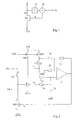
- FIG. 1 schematically represents a controlled resistor according to the invention produced according to this principle. It includes a MOS transistor M1 whose gate g is connected to the output of an adder 10 receiving on a first input the control voltage Vc and on a second input the voltage present on the drain d of the transistor M1 via d 'a circuit 12 which multiplies this drain voltage by the factor k. All the voltages (Vc, the drain voltage, the gate voltage) are referenced with respect to the source s of the transistor M1.
- Id K [(Vgd-Vt 2 ) Vds - 1 ⁇ 2Vds 2 ]
- Vgd the voltage between the gate g and the electrode d which has become the source
- the adder 10 supplies a voltage Vgs which is always referenced with respect to the electrode s.
- FIG. 2 represents a practical embodiment of a controlled resistor according to the invention.
- This controlled resistor includes an N-channel MOS transistor MN1 disposed in a divider bridge.
- the source s of transistor MN1 is connected to ground GND and its drain d is connected by a resistor 14 to a voltage to be divided Vin.
- the output voltage Vd of the bridge is taken from the drain of transistor MN1.
- the gate g of the transistor MN1 is controlled by the output of an operational amplifier 16 conventionally mounted as an adder.
- the voltages to be added are supplied to the non-inverting input of the amplifier 16 via respective resistors 18 and 19.
- This non-inverting input is also connected to ground GND by a resistor 20.
- the inverting input of the amplifier 16 is connected to the output of the amplifier by a resistor 21 and to the ground by a resistor 22.
- the control voltage Vc is applied to the amplifier 16 via the resistor 18.
- Vd voltage of the drain of the transistor MN1
- the amplifier 16 is unable to process it.
- the input impedance of the amplifier 16 (depending on the resistors 18 to 20) is not negligible compared to the resistors of the divider bridge (MN1, 14) and could therefore disturb the operation of the bridge.
- the drain voltage is shifted upwards by a base-emitter voltage Vbe thanks to a PNP transistor Q1 mounted as a follower.
- the emitter of transistor Q1 is connected to resistor 19 and polarized by means of a current source MP1 connected to a high supply potential Vdd.
- the collector of transistor Q1 is connected to ground.
- a PNP transistor Q2 is provided to compensate for this offset.
- the transistor Q2 is mounted as a diode. Its base and its collector are connected to ground and its transmitter is connected to the voltage Vdd via a current source MP2.
- the inverting input of the amplifier 16 is connected to the emitter of the transistor Q2 via a resistor 23 of the same value as the resistor 22.
- the transistors Q1 and Q2 can be replaced by MOS transistors with P channel , whose substrates are connected to the sources.
- the diodes may be available. series on the emitter of transistor Q1, the same number of diodes being arranged in series with transistor Q2.
- the coefficient k is set to 1 by choosing all the resistors 18 to 22 of the same value. In the case where the input voltage Vin is always positive, the coefficient k is set to 1 ⁇ 2 by choosing the resistor 19 by a value three times greater than that of the resistor 18, the values of the resistors 20 to 23 being equal to that of resistance 18.
- the current sources MP1 and MP2 are constituted by P-channel MOS transistors whose gate is controlled by a reference voltage Vref.
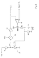
- FIG. 3 shows an example of the use of a controlled resistor according to the present invention.
- the controlled resistor, 30, is inserted into a divider bridge as in FIG. 2.
- the output voltage Vd of the bridge is supplied to an amplifier 32 via an adder 34 which superimposes on the voltage Vd a mode voltage common Vmc.
- the output voltage Vout of the amplifier 32 is applied to the inverting input of a comparator 36.
- the non-inverting input of this comparator receives the common mode voltage Vmc increased by a limit voltage VL.
- the output of comparator 36 is connected to the gate of a P-channel MP3 MOS transistor whose source is connected to the supply potential Vdd and the drain is connected to ground GND by a resistor bridge R1, R2.
- This resistance bridge supplies the control voltage Vc of the resistor 30.
- a capacitor C1 is connected to ground, in parallel on the resistor R2.
- the comparator 36 turns on the transistor MP3 which starts to charge the capacitor C1 via the resistor R1.
- the control voltage Vc increases and the value of the resistance 30 decreases accordingly.
- the voltage Vd therefore begins to decrease until it becomes lower than the limit voltage VL.
- the comparator 36 turns the MP3 transistor off and the capacitor C1 discharges slowly into the resistor R2.
- the resistance 30 increases and the voltage Vd increases until this voltage Vd again exceeds the limit voltage VL, and so on.
Landscapes
- Amplifiers (AREA)
- Networks Using Active Elements (AREA)
Applications Claiming Priority (2)
| Application Number | Priority Date | Filing Date | Title |
|---|---|---|---|
| FR9412570 | 1994-10-17 | ||
| FR9412570A FR2725856A1 (fr) | 1994-10-17 | 1994-10-17 | Resistance commandee en tension |
Publications (2)
| Publication Number | Publication Date |
|---|---|
| EP0708526A1 true EP0708526A1 (de) | 1996-04-24 |
| EP0708526B1 EP0708526B1 (de) | 2000-05-03 |
Family
ID=9468064
Family Applications (1)
| Application Number | Title | Priority Date | Filing Date |
|---|---|---|---|
| EP19950410117 Expired - Lifetime EP0708526B1 (de) | 1994-10-17 | 1995-10-12 | Spannungsgesteuerter Widerstand |
Country Status (3)
| Country | Link |
|---|---|
| EP (1) | EP0708526B1 (de) |
| DE (1) | DE69516627T2 (de) |
| FR (1) | FR2725856A1 (de) |
Cited By (2)
| Publication number | Priority date | Publication date | Assignee | Title |
|---|---|---|---|---|
| CN100514841C (zh) * | 2002-11-08 | 2009-07-15 | 广达电脑股份有限公司 | 单向导通装置 |
| EP2093882A1 (de) * | 2008-02-21 | 2009-08-26 | Siemens Milltronics Process Instruments Inc. | Schaltung eines variablen Verstärkers |
Families Citing this family (1)
| Publication number | Priority date | Publication date | Assignee | Title |
|---|---|---|---|---|
| JP2025159995A (ja) * | 2024-04-09 | 2025-10-22 | 株式会社東芝 | 半導体集積回路 |
Citations (3)
| Publication number | Priority date | Publication date | Assignee | Title |
|---|---|---|---|---|
| DE2403756A1 (de) * | 1974-01-26 | 1975-08-07 | Licentia Gmbh | Schaltung fuer einen elektronisch steuerbaren widerstand |
| EP0220043A2 (de) * | 1985-10-15 | 1987-04-29 | Ray Milton Dolby | Schaltungsanordnungen zum Erhalt einer gewünschten Konduktanz-Kennlinie unter Verwendung eines Feldeffekttransistors |
| US4868519A (en) * | 1988-11-02 | 1989-09-19 | Dnic Brokerage Company | Microprocessor-controlled amplifier |
-
1994
- 1994-10-17 FR FR9412570A patent/FR2725856A1/fr active Granted
-
1995
- 1995-10-12 EP EP19950410117 patent/EP0708526B1/de not_active Expired - Lifetime
- 1995-10-12 DE DE1995616627 patent/DE69516627T2/de not_active Expired - Fee Related
Patent Citations (3)
| Publication number | Priority date | Publication date | Assignee | Title |
|---|---|---|---|---|
| DE2403756A1 (de) * | 1974-01-26 | 1975-08-07 | Licentia Gmbh | Schaltung fuer einen elektronisch steuerbaren widerstand |
| EP0220043A2 (de) * | 1985-10-15 | 1987-04-29 | Ray Milton Dolby | Schaltungsanordnungen zum Erhalt einer gewünschten Konduktanz-Kennlinie unter Verwendung eines Feldeffekttransistors |
| US4868519A (en) * | 1988-11-02 | 1989-09-19 | Dnic Brokerage Company | Microprocessor-controlled amplifier |
Cited By (2)
| Publication number | Priority date | Publication date | Assignee | Title |
|---|---|---|---|---|
| CN100514841C (zh) * | 2002-11-08 | 2009-07-15 | 广达电脑股份有限公司 | 单向导通装置 |
| EP2093882A1 (de) * | 2008-02-21 | 2009-08-26 | Siemens Milltronics Process Instruments Inc. | Schaltung eines variablen Verstärkers |
Also Published As
| Publication number | Publication date |
|---|---|
| FR2725856B1 (de) | 1997-02-21 |
| DE69516627T2 (de) | 2001-01-25 |
| EP0708526B1 (de) | 2000-05-03 |
| FR2725856A1 (fr) | 1996-04-19 |
| DE69516627D1 (de) | 2000-06-08 |
Similar Documents
| Publication | Publication Date | Title |
|---|---|---|
| EP0438363B1 (de) | Strommess-Schaltung in einem MOS-Leistungstransistor | |
| US5397934A (en) | Apparatus and method for adjusting the threshold voltage of MOS transistors | |
| US5614851A (en) | High-accuracy, low-power peak-to-peak voltage detector | |
| US7528648B2 (en) | Replica biased system | |
| EP0969344A2 (de) | Integrierte Halbleiterschaltung mit Spannungsfolgerschaltung | |
| US4763028A (en) | Circuit and method for semiconductor leakage current compensation | |
| EP0414319A1 (de) | Schaltung für die Lieferung einer Referenzspannung | |
| FR3102580A1 (fr) | Régulateur de tension | |
| FR2820904A1 (fr) | Dispositif generateur d'une tension de reference precise | |
| EP0613241B1 (de) | Ausgangsgleichtaktspannungssteuerungseinrichtung für ausbalancierten Verstärker | |
| EP0708526B1 (de) | Spannungsgesteuerter Widerstand | |
| US5465041A (en) | Bipolar tracking current source/sink with ground clamp | |
| EP0638996A1 (de) | Chopper-Differenzverstärker mit MOS-Kondensatoren | |
| US4656435A (en) | Constant biasing circuit and operational amplifier using said circuit | |
| US4689678A (en) | Gradation distortion compensation by FET pre-emphasis circuit operating in FET saturation region | |
| FR2969328A1 (fr) | Circuit de generation d'une tension de reference sous une faible tension d'alimentation | |
| EP0441716A1 (de) | Spannungsgesteuerter Widerstand | |
| EP0050583B1 (de) | Wechselspannung/Gleichstrom-Konverter und Schwingkreis-Schaltung mit einem solchen Konverter | |
| FR2757964A1 (fr) | Regulateur de tension serie | |
| EP0843408B1 (de) | Verstärkerschaltung mit Eingangsstromkompensationsvorrichtung | |
| EP0332548B1 (de) | Stabilisierter Generator für die Lieferung einer Schwellenspannung für einen MOS-Transistor | |
| EP1102148B1 (de) | Niedrigtemperaturkorrigierte Spannungsgeneratoreinrichtung | |
| JP2000155139A (ja) | 電流検出装置 | |
| JP3031334B2 (ja) | 固体撮像装置およびその出力回路 | |
| EP0700162A1 (de) | Logische Schaltung mit Differenzstufen |
Legal Events
| Date | Code | Title | Description |
|---|---|---|---|
| PUAI | Public reference made under article 153(3) epc to a published international application that has entered the european phase |
Free format text: ORIGINAL CODE: 0009012 |
|
| AK | Designated contracting states |
Kind code of ref document: A1 Designated state(s): DE FR GB IT |
|
| RIN1 | Information on inventor provided before grant (corrected) |
Inventor name: BERNARD, CHRISTOPHE Inventor name: BERNARD, PATRICK |
|
| 17P | Request for examination filed |
Effective date: 19961002 |
|
| RAP3 | Party data changed (applicant data changed or rights of an application transferred) |
Owner name: STMICROELECTRONICS S.A. |
|
| GRAG | Despatch of communication of intention to grant |
Free format text: ORIGINAL CODE: EPIDOS AGRA |
|
| 17Q | First examination report despatched |
Effective date: 19990624 |
|
| GRAG | Despatch of communication of intention to grant |
Free format text: ORIGINAL CODE: EPIDOS AGRA |
|
| GRAH | Despatch of communication of intention to grant a patent |
Free format text: ORIGINAL CODE: EPIDOS IGRA |
|
| GRAH | Despatch of communication of intention to grant a patent |
Free format text: ORIGINAL CODE: EPIDOS IGRA |
|
| GRAA | (expected) grant |
Free format text: ORIGINAL CODE: 0009210 |
|
| AK | Designated contracting states |
Kind code of ref document: B1 Designated state(s): DE FR GB IT |
|
| REF | Corresponds to: |
Ref document number: 69516627 Country of ref document: DE Date of ref document: 20000608 |
|
| GBT | Gb: translation of ep patent filed (gb section 77(6)(a)/1977) |
Effective date: 20000525 |
|
| ITF | It: translation for a ep patent filed | ||
| PLBE | No opposition filed within time limit |
Free format text: ORIGINAL CODE: 0009261 |
|
| STAA | Information on the status of an ep patent application or granted ep patent |
Free format text: STATUS: NO OPPOSITION FILED WITHIN TIME LIMIT |
|
| 26N | No opposition filed | ||
| REG | Reference to a national code |
Ref country code: GB Ref legal event code: IF02 |
|
| PGFP | Annual fee paid to national office [announced via postgrant information from national office to epo] |
Ref country code: DE Payment date: 20041007 Year of fee payment: 10 |
|
| PGFP | Annual fee paid to national office [announced via postgrant information from national office to epo] |
Ref country code: FR Payment date: 20050825 Year of fee payment: 11 |
|
| PG25 | Lapsed in a contracting state [announced via postgrant information from national office to epo] |
Ref country code: IT Free format text: LAPSE BECAUSE OF NON-PAYMENT OF DUE FEES Effective date: 20051012 |
|
| PGFP | Annual fee paid to national office [announced via postgrant information from national office to epo] |
Ref country code: GB Payment date: 20051012 Year of fee payment: 11 |
|
| PG25 | Lapsed in a contracting state [announced via postgrant information from national office to epo] |
Ref country code: DE Free format text: LAPSE BECAUSE OF NON-PAYMENT OF DUE FEES Effective date: 20060503 |
|
| GBPC | Gb: european patent ceased through non-payment of renewal fee |
Effective date: 20061012 |
|
| REG | Reference to a national code |
Ref country code: FR Ref legal event code: ST Effective date: 20070629 |
|
| PG25 | Lapsed in a contracting state [announced via postgrant information from national office to epo] |
Ref country code: GB Free format text: LAPSE BECAUSE OF NON-PAYMENT OF DUE FEES Effective date: 20061012 |
|
| PG25 | Lapsed in a contracting state [announced via postgrant information from national office to epo] |
Ref country code: FR Free format text: LAPSE BECAUSE OF NON-PAYMENT OF DUE FEES Effective date: 20061031 |