EP0414319A1 - Schaltung für die Lieferung einer Referenzspannung - Google Patents
Schaltung für die Lieferung einer Referenzspannung Download PDFInfo
- Publication number
- EP0414319A1 EP0414319A1 EP90202235A EP90202235A EP0414319A1 EP 0414319 A1 EP0414319 A1 EP 0414319A1 EP 90202235 A EP90202235 A EP 90202235A EP 90202235 A EP90202235 A EP 90202235A EP 0414319 A1 EP0414319 A1 EP 0414319A1
- Authority
- EP
- European Patent Office
- Prior art keywords
- transistor
- whose
- voltage
- input
- collector
- Prior art date
- Legal status (The legal status is an assumption and is not a legal conclusion. Google has not performed a legal analysis and makes no representation as to the accuracy of the status listed.)
- Granted
Links
- 230000001105 regulatory effect Effects 0.000 description 2
- 241001529544 Riccardia Species 0.000 description 1
- 238000010586 diagram Methods 0.000 description 1
Images

Classifications
-
- G—PHYSICS
- G05—CONTROLLING; REGULATING
- G05F—SYSTEMS FOR REGULATING ELECTRIC OR MAGNETIC VARIABLES
- G05F1/00—Automatic systems in which deviations of an electric quantity from one or more predetermined values are detected at the output of the system and fed back to a device within the system to restore the detected quantity to its predetermined value or values, i.e. retroactive systems
- G05F1/10—Regulating voltage or current
-
- G—PHYSICS
- G05—CONTROLLING; REGULATING
- G05F—SYSTEMS FOR REGULATING ELECTRIC OR MAGNETIC VARIABLES
- G05F1/00—Automatic systems in which deviations of an electric quantity from one or more predetermined values are detected at the output of the system and fed back to a device within the system to restore the detected quantity to its predetermined value or values, i.e. retroactive systems
- G05F1/10—Regulating voltage or current
- G05F1/46—Regulating voltage or current wherein the variable actually regulated by the final control device is DC
- G05F1/56—Regulating voltage or current wherein the variable actually regulated by the final control device is DC using semiconductor devices in series with the load as final control devices
- G05F1/565—Regulating voltage or current wherein the variable actually regulated by the final control device is DC using semiconductor devices in series with the load as final control devices sensing a condition of the system or its load in addition to means responsive to deviations in the output of the system, e.g. current, voltage, power factor
-
- Y—GENERAL TAGGING OF NEW TECHNOLOGICAL DEVELOPMENTS; GENERAL TAGGING OF CROSS-SECTIONAL TECHNOLOGIES SPANNING OVER SEVERAL SECTIONS OF THE IPC; TECHNICAL SUBJECTS COVERED BY FORMER USPC CROSS-REFERENCE ART COLLECTIONS [XRACs] AND DIGESTS
- Y10—TECHNICAL SUBJECTS COVERED BY FORMER USPC
- Y10S—TECHNICAL SUBJECTS COVERED BY FORMER USPC CROSS-REFERENCE ART COLLECTIONS [XRACs] AND DIGESTS
- Y10S323/00—Electricity: power supply or regulation systems
- Y10S323/901—Starting circuits
Definitions
- the invention relates to a circuit for supplying a reference voltage, comprising a voltage generator having a supply terminal and an output for delivering a voltage of given nominal value and comprising a differential amplifier presenting a supply terminal for a source. of supply voltage, a non-inverting input connected to the output of the voltage generator, an inverting input and an output as well as a first output follower stage, the output of which delivers said reference voltage is retro-coupled to the inverting input of the amplifier via a divider bridge.
- the voltage generator is liable, when it is switched on, to give rise to instabilities.
- the invention relates to a circuit making it possible to avoid this drawback.
- the basic idea of the invention consists in transmitting the voltage generator signal only when the supply voltage is sufficient for the region of possible instabilities to be exceeded.
- the circuit according to the invention is for this purpose characterized in that the output of the differential amplifier is connected to the input of the first follower stage through a controlled switching device, the first follower stage having its input connected to terminal d supply through a first resistor, and having its output connected to the supply terminal of the voltage generator and in that it comprises a control circuit for the switching device arranged to receive at least the supply voltage so that the switching device is closed when the first supply voltage reaches a threshold for which both the voltage generator and the differential amplifier are in a nominal operating zone .
- the voltage generator is supplied by the reference voltage produced by the circuit, and the reference voltage, once the switching device is closed, is 1 / k times higher than the voltage produced by the voltage generator, k being the division ratio of the first divider bridge.
- the first supply voltage has a low value, insufficient for the switching device to be closed, the voltage at the output of the circuit, which also supplies the voltage generator, varies with the same slope as the first supply voltage, at a constant close.
- the output voltage curve as a function of the first supply voltage therefore no longer presents a risk of instability.
- control circuit and the controlled switching circuit cooperate directly with the differential amplifier. This makes it possible to simplify the electronic diagram.
- the differential amplifier may include a first branch, the input of which is said non-inverting input and a second branch, the input of which is said inverting input, the control circuit can be arranged to inhibit the passage of current through the second branch when the supply voltage is lower than said threshold, and the controlled switching circuit may include a second follower stage which is arranged to be conductive only when current flows through the second branch.
- the first branch may include the emitter-collector path of a first transistor of a first type, the base and the collector of which are connected respectively to the emitter and to the base of a second transistor of the first type whose collector is connected to a second supply voltage source, the collector of the first transistor being connected to that of a third transistor of the second type opposite to the first, the emitter of which is connected to the second voltage source d power supply through a second resistor and the base of which constitutes the non-inverting input of the differential amplifier.
- Such a branch has a structure such that it derives from the current from low levels of the first supply voltage.
- the second branch may include the emitter-collector path of a fourth transistor of the first type, the base of which is connected to that of the first transistor, the collector of the fourth transistor being connected to that of a fifth transistor of the second type, the emitter of which is connected to that of the third transistor and whose base constitutes the inverting input of the differential amplifier.
- Such a branch has a structure such that it derives from the current only from a relatively high significant level of the first supply voltage.
- the fourth transistor can have its emitter connected to that of the first transistor.
- control circuit is advantageously common to the two branches.
- the control circuit may include a sixth transistor of the second type, the collector of which is connected to the first supply voltage source, the emitter of which is connected to the emitters of the first and fourth transistors, and the base of which is connected to the terminal of the first resistor which is not connected to the first source of supply voltage.
- the voltage on the basis of the sixth transistor determines the threshold from which the differential amplifier produces an output signal.
- the second follower stage may include a seventh transistor whose base is connected to the collector of the fifth transistor, whose collector is connected to the second supply voltage source and whose emitter is connected to the input of the first follower stage, possibly via a live diode.
- the value of said threshold can be chosen more precisely by having a second resistance between the first resistance and the input of the first follower stage.
- the first follower stage advantageously comprises an eighth transistor with two emitters, the base of which constitutes the input, the collector of which is connected to the first supply voltage source, the first emitter of which is connected to one end of the bridge and the second of which transmitter constitutes the output of the first follower stage.
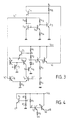
- a voltage generator REF delivers a voltage V R which is applied to the non-inverting input of a differential amplifier A supplied with a supply voltage V cc .
- the output S of the amplifier A drives a follower circuit T whose output, which delivers a regulated reference voltage V O is retro-coupled to the inverting input of the amplifier A via a resistive divider bridge R3, R4.
- the REF voltage generator is supplied by the supply voltage V cc .
- the voltage generator REF delivers a voltage V at the output + i which is applied to the non-inverting input of the differential amplifier A supplied with a supply voltage V cc .
- the output S of the amplifier A is connected via a controlled switching device 1 to the input S ′ of the follower circuit.
- a re sistance R1 is arranged between the input S ′ and the supply voltage source V cc .
- the output of the follower circuit delivers the regulated reference voltage V O. This output is looped over the inverting input of amplifier A (signal V - i ) using a divider bridge comprising resistors R3 and R4.
- the signal V - i is present at the common point (or midpoint) of the divider bridge.
- the other end of the divider point is connected to a second source of supply voltage (here the common mode pole).
- the follower circuit is represented as a transistor T whose base is the point S ′, whose emitter delivers the signal V O and whose collector is connected to the supply voltage source V cc .
- the signal V O is applied to the supply terminal of the voltage generator REF.
- a control circuit C which receives the supply voltage Vcc (and optionally the voltage V O ) is arranged so as to close the switching device 1 when the supply voltage V cc exceeds a given threshold for which the voltage V + i delivered by the REF voltage generator has exceeded the portion of its characteristic in which instabilities may occur.
- the supply voltage V cc starts from the value 0 and increases to reach its nominal value.
- the switching current 1 is open and the voltage V O changes in proportion to the instantaneous value of the voltage V cc and independently of the voltage V + i .
- the input S ′ of the follower stage is referenced to the potential V cc through the resistor R1.
- V + i reaches its nominal value V REF .
- a voltage generator (known as of the "band gap" type) described in the aforementioned book p.295, comprises a transistor T11 of the npn type whose collector is connected to the aforementioned point B and which has a resistance R15, acting as a current source, between its collector and its base.
- the emitter of transistor T11 which delivers the voltage V + i is connected to a diode (npn transistor T12 mounted as a diode by base-collector short-circuit) through a resistor R11.
- the emitter of transistor T12 is connected to the common mode pole, and its base to that of a transistor T14 whose emitter is connected to the common mode pole through a resistor R14 and whose collector is firstly connected to the transistor emitter T11 through a resistor R16 and on the other hand connected to the base of an npn transistor T15 whose emitter is connected to the common mode pole, and whose collector is connected to the transistor base T11.
- Amplifier A comprises a first branch having a transistor T type of pnp type whose emitter is connected to a point F, whose base is connected to the emitter of a transistor T7 of pnp type, whose collector is connected to common mode pole and whose base is connected to the transistor collector T5.
- the collector of transistor T5 is connected to that of a transistor T8 of npn type, the base of which is attacked by voltage V + i available on the emitter of transistor T11, and whose emitter is connected to the common mode pole through a resistor R8.
- the transistors T5 and T7 have two emitter-base junctions in series, which means that a current is likely to flow in the first branch even for a low potential value at point F.
- the second branch has a pnp transistor T6 whose emitter is connected to point F, whose base is connected to that of transistor T du and whose collector (point S) is connected to that of an npn transistor T9 whose emitter is connected to the common mode pole through the resistor R8.
- the control circuit includes an npn transistor T3 whose collector is connected to the supply voltage source V cc , whose emitter is connected to said point F and whose base is preferably connected to the mid point H of a bridge divider R1, R2 having two resistors R1 and R2 in series between the supply voltage source V cc and the point S ′, or directly at the point S ′, the resistance R2 being omitted.
- the switching circuit includes a pnp transistor T10 whose base is connected to point S (output of amplifier A), whose collector is connected to the common mode pole and whose emitter is connected to point S ′ through a live diode D.
- the output follower stage comprises a transistor (T1, T2) with two emitters (or two transistors T1 and T2 mounted as a follower emitter), the emitter of T1 connected to the divider bridge (R3, R4) and that of T2 delivering the voltage V o at point B.
- T1, T2 with two emitters (or two transistors T1 and T2 mounted as a follower emitter), the emitter of T1 connected to the divider bridge (R3, R4) and that of T2 delivering the voltage V o at point B.
- V cc When V cc has a value below the given threshold, the first branch of the amplifier is likely to be crossed by a current, but the second branch is not crossed by any current. The transistor T10 is then blocked. The base of the transistors T1 and T2 is then at a potential very close to the instantaneous value of V cc .
- V + i ⁇ V REF that is to say that for the calculation, it is considered that the voltage threshold corresponds practically to the correct operating threshold of the voltage generator. He comes : For the amplifier described, correct operation requires that V H is at least equal to 5V D (in fact it is necessary that V H is significantly greater than this value). We then have: V cco ⁇ 5V D + R1 R2 [4V D - (1 + R3 R4 ) V ref ] The report R1 R2 therefore makes it possible to determine the threshold V ccO of V cc from which the switching circuit is closed.
- the base of the transistor T3 is connected to the midpoint H ′ of a divider bridge R′1 and R′2 disposed between the voltage source V cc and the common mode pole.
- the base of the transistor T1 is connected to the voltage source V cc through the resistor R1.
- the emitter of transistor T3 is connected to point C, that of transistor T1 is connected to point A through resistor R3, and that of transistor T2 is connected to point B.
- the rest of the circuit is as in Figure 3. We have The threshold condition is then: V H ′ > 5V D
- V cco ⁇ 5 V D (1 + ) The report determines the threshold V cco of V cc from which the switching circuit is closed.
- the voltages V + i , V - i and V0 increase as soon as V cc reaches V D (0.7 V), the regulation being obtained from 6 V D (approximately 4.2 V).
Landscapes
- Engineering & Computer Science (AREA)
- Physics & Mathematics (AREA)
- Electromagnetism (AREA)
- General Physics & Mathematics (AREA)
- Radar, Positioning & Navigation (AREA)
- Automation & Control Theory (AREA)
- Amplifiers (AREA)
- Continuous-Control Power Sources That Use Transistors (AREA)
Applications Claiming Priority (2)
| Application Number | Priority Date | Filing Date | Title |
|---|---|---|---|
| FR8911114A FR2651343A1 (fr) | 1989-08-22 | 1989-08-22 | Circuit destine a fournir une tension de reference. |
| FR8911114 | 1989-08-22 |
Publications (2)
| Publication Number | Publication Date |
|---|---|
| EP0414319A1 true EP0414319A1 (de) | 1991-02-27 |
| EP0414319B1 EP0414319B1 (de) | 1994-08-03 |
Family
ID=9384840
Family Applications (1)
| Application Number | Title | Priority Date | Filing Date |
|---|---|---|---|
| EP90202235A Expired - Lifetime EP0414319B1 (de) | 1989-08-22 | 1990-08-20 | Schaltung für die Lieferung einer Referenzspannung |
Country Status (6)
| Country | Link |
|---|---|
| US (1) | US5079497A (de) |
| EP (1) | EP0414319B1 (de) |
| JP (1) | JP2790364B2 (de) |
| KR (1) | KR0154335B1 (de) |
| DE (1) | DE69011239T2 (de) |
| FR (1) | FR2651343A1 (de) |
Cited By (1)
| Publication number | Priority date | Publication date | Assignee | Title |
|---|---|---|---|---|
| EP0638857A1 (de) * | 1993-08-13 | 1995-02-15 | Motorola Semiconducteurs S.A. | Schaltung zur Verwendung mit einer Rückkopplungsanordnung |
Families Citing this family (23)
| Publication number | Priority date | Publication date | Assignee | Title |
|---|---|---|---|---|
| JP2727809B2 (ja) * | 1991-08-26 | 1998-03-18 | 日本電気株式会社 | 半導体集積回路 |
| JP3337079B2 (ja) * | 1991-11-26 | 2002-10-21 | ローム株式会社 | 電源回路 |
| JP2901434B2 (ja) * | 1992-09-30 | 1999-06-07 | シャープ株式会社 | 直流安定化電源装置 |
| WO1994012921A1 (en) * | 1992-12-03 | 1994-06-09 | Motorola, Inc. | Digital voltage regulator having capacitance selector |
| US5604466A (en) * | 1992-12-08 | 1997-02-18 | International Business Machines Corporation | On-chip voltage controlled oscillator |
| US5486778A (en) * | 1993-03-10 | 1996-01-23 | Brooktree Corporation | Input buffer for translating TTL levels to CMOS levels |
| US5583442A (en) * | 1994-02-03 | 1996-12-10 | Harris Corporation | Differential voltage monitor using a bridge circuit with resistors on and off of an integrated circuit |
| JPH09128080A (ja) * | 1995-08-30 | 1997-05-16 | Sgs Thomson Microelectron Inc | 電圧調整器回路 |
| FR2750240B1 (fr) * | 1996-06-20 | 1998-07-31 | Sgs Thomson Microelectronics | Generateur de reference de tension |
| JP3322145B2 (ja) * | 1996-12-26 | 2002-09-09 | 株式会社村田製作所 | 電流制御回路 |
| KR100735440B1 (ko) * | 1998-02-13 | 2007-10-24 | 로무 가부시키가이샤 | 반도체장치 및 자기디스크장치 |
| KR100533389B1 (ko) * | 1998-09-28 | 2006-02-08 | 매그나칩 반도체 유한회사 | 클럭동기식기준전압발생기 |
| JP4225630B2 (ja) * | 1999-05-27 | 2009-02-18 | 株式会社ルネサステクノロジ | 電圧発生回路 |
| US6175223B1 (en) * | 1999-09-04 | 2001-01-16 | Texas Instruments Incorporated | Controlled linear start-up in a linear regulator |
| US6353310B1 (en) * | 2000-03-09 | 2002-03-05 | Tongt-Huei Wang | DC/DC charge and supply converting module |
| US6528975B2 (en) * | 2000-12-15 | 2003-03-04 | Tropian Inc. | Saturation prevention and amplifier distortion reduction |
| US7439718B2 (en) * | 2004-09-30 | 2008-10-21 | Freescale Semiconductor, Inc. | Apparatus and method for high speed voltage regulation |
| CA2628255C (en) * | 2005-10-31 | 2016-04-19 | The Regents Of The University Of Michigan | Compositions and methods for treating and diagnosing cancer |
| US8331882B1 (en) | 2007-06-22 | 2012-12-11 | Panasonic Corporation | VSWR normalizing envelope modulator |
| US7554395B1 (en) | 2007-06-28 | 2009-06-30 | Panasonic Corporation | Automatic low battery compensation scaling across multiple power amplifier stages |
| US7702300B1 (en) | 2007-07-12 | 2010-04-20 | Panasonic Corporation | Envelope modulator saturation detection using a DC-DC converter |
| JP6772355B1 (ja) | 2019-10-15 | 2020-10-21 | 株式会社京三製作所 | スイッチングモジュール |
| US11522572B1 (en) * | 2021-05-18 | 2022-12-06 | Qualcomm Incorporated | Audio non-linearity cancellation for switches for audio and other applications |
Citations (3)
| Publication number | Priority date | Publication date | Assignee | Title |
|---|---|---|---|---|
| EP0019095A1 (de) * | 1979-05-18 | 1980-11-26 | International Business Machines Corporation | Schaltungen für geregelte Spannungsquelle |
| WO1986005604A1 (en) * | 1985-03-13 | 1986-09-25 | Analog Devices, Inc. | Voltage/current source |
| EP0226725A1 (de) * | 1985-11-13 | 1987-07-01 | AKO-Werke GmbH & Co | Stabilisierungsschaltung für einen Mikrocomputer |
Family Cites Families (5)
| Publication number | Priority date | Publication date | Assignee | Title |
|---|---|---|---|---|
| US3743923A (en) * | 1971-12-02 | 1973-07-03 | Rca Corp | Reference voltage generator and regulator |
| JPS5543643A (en) * | 1978-09-21 | 1980-03-27 | Toshiba Corp | Constant voltage circuit |
| US4368420A (en) * | 1981-04-14 | 1983-01-11 | Fairchild Camera And Instrument Corp. | Supply voltage sense amplifier |
| US4400661A (en) * | 1981-10-02 | 1983-08-23 | Ncr Corporation | Voltage regulation and battery dissipation limiter circuit |
| JPS5999510A (ja) * | 1982-11-30 | 1984-06-08 | Fujitsu Ltd | 定電圧回路 |
-
1989
- 1989-08-22 FR FR8911114A patent/FR2651343A1/fr active Pending
-
1990
- 1990-08-14 US US07/567,415 patent/US5079497A/en not_active Expired - Fee Related
- 1990-08-20 JP JP2217235A patent/JP2790364B2/ja not_active Expired - Lifetime
- 1990-08-20 DE DE69011239T patent/DE69011239T2/de not_active Expired - Fee Related
- 1990-08-20 EP EP90202235A patent/EP0414319B1/de not_active Expired - Lifetime
- 1990-08-21 KR KR1019900012857A patent/KR0154335B1/ko not_active Expired - Fee Related
Patent Citations (3)
| Publication number | Priority date | Publication date | Assignee | Title |
|---|---|---|---|---|
| EP0019095A1 (de) * | 1979-05-18 | 1980-11-26 | International Business Machines Corporation | Schaltungen für geregelte Spannungsquelle |
| WO1986005604A1 (en) * | 1985-03-13 | 1986-09-25 | Analog Devices, Inc. | Voltage/current source |
| EP0226725A1 (de) * | 1985-11-13 | 1987-07-01 | AKO-Werke GmbH & Co | Stabilisierungsschaltung für einen Mikrocomputer |
Non-Patent Citations (1)
| Title |
|---|
| NEW ELECTRONICS INCORPORATING ELECTRONICS TODAY vol. 17, no. 16, août 1984, LONDON GB page 23 M.A. BURNS: "LOW QUIESCENT CURRENT REGULATOR" * |
Cited By (3)
| Publication number | Priority date | Publication date | Assignee | Title |
|---|---|---|---|---|
| EP0638857A1 (de) * | 1993-08-13 | 1995-02-15 | Motorola Semiconducteurs S.A. | Schaltung zur Verwendung mit einer Rückkopplungsanordnung |
| FR2709005A1 (fr) * | 1993-08-13 | 1995-02-17 | Motorola Semiconducteurs | Circuit destiné à une utilisation avec un agencement de retour. |
| US5471167A (en) * | 1993-08-13 | 1995-11-28 | Motorola, Inc. | Circuit for use with a feedback arrangement |
Also Published As
| Publication number | Publication date |
|---|---|
| FR2651343A1 (fr) | 1991-03-01 |
| KR910005125A (ko) | 1991-03-30 |
| DE69011239D1 (de) | 1994-09-08 |
| US5079497A (en) | 1992-01-07 |
| EP0414319B1 (de) | 1994-08-03 |
| JP2790364B2 (ja) | 1998-08-27 |
| KR0154335B1 (ko) | 1998-12-15 |
| JPH03103908A (ja) | 1991-04-30 |
| DE69011239T2 (de) | 1995-02-23 |
Similar Documents
| Publication | Publication Date | Title |
|---|---|---|
| EP0414319B1 (de) | Schaltung für die Lieferung einer Referenzspannung | |
| EP0816964B1 (de) | Spannungsregelungsvorrichtung mit geringer interner Verlustleistung | |
| EP0511707B1 (de) | Kaskodendifferenzverstärker | |
| EP0587509B1 (de) | Spannungs-Strom-Umsetzerschaltungsanordnung | |
| EP0700151A1 (de) | Leistungsfolgeverstärkerstufe | |
| EP0649079A1 (de) | Geregelter Spannungsquellengenerator der Bandgapbauart | |
| EP1294095A2 (de) | Strombegrenzende logische Schnittstellenschaltung | |
| EP0376383B1 (de) | Integrierte Schaltung mit einem schaltbaren Stromquellengenerator | |
| EP0554196A1 (de) | Telefonleitungsstrommodulator | |
| EP0219158B1 (de) | Spannungsregelungsschaltung | |
| EP0533230B1 (de) | Differenzverstärker, Oszillator und Mischer | |
| FR2744299A1 (fr) | Convertisseur continu/continu a faible tension d'alimentation | |
| EP0655176B1 (de) | Verstärkerstufe mit geringer thermischer verzerrung | |
| EP0355922B1 (de) | Eingangsschaltung mit beschleunigtem Schalten | |
| EP0353808B1 (de) | Stromausgleichsschaltung | |
| EP0886382A1 (de) | Analog-Digital-Wandler | |
| FR2688361A1 (fr) | Etage de sortie push-pull pour amplificateur en circuit integre. | |
| EP0722217B1 (de) | Vorrichtung zur Einstellung der Dämpfung eines Signals | |
| EP0838901B1 (de) | Analog-Digital-Wandlungsgerät mit geregelter Eingangsdynamik | |
| EP0479377A1 (de) | Stromquelle mit bestimmtem Verhältnis zwischen Eingangs- und Ausgangsströmen | |
| EP0292070A1 (de) | Stromspiegel mit hoher Ausgangsspannung | |
| EP0122820B1 (de) | Regler für einen Batterieladegenerator | |
| JP3843481B2 (ja) | サンプルホールド回路 | |
| FR2642918A1 (fr) | Circuit amplificateur large bande a controle automatique de gain | |
| FR2669790A1 (fr) | Circuit integre presentant un generateur de courant commutable. |
Legal Events
| Date | Code | Title | Description |
|---|---|---|---|
| PUAI | Public reference made under article 153(3) epc to a published international application that has entered the european phase |
Free format text: ORIGINAL CODE: 0009012 |
|
| AK | Designated contracting states |
Kind code of ref document: A1 Designated state(s): DE FR GB IT |
|
| 17P | Request for examination filed |
Effective date: 19910808 |
|
| RAP1 | Party data changed (applicant data changed or rights of an application transferred) |
Owner name: N.V. PHILIPS' GLOEILAMPENFABRIEKEN Owner name: PHILIPS COMPOSANTS |
|
| 17Q | First examination report despatched |
Effective date: 19931011 |
|
| GRAA | (expected) grant |
Free format text: ORIGINAL CODE: 0009210 |
|
| AK | Designated contracting states |
Kind code of ref document: B1 Designated state(s): DE FR GB IT |
|
| REF | Corresponds to: |
Ref document number: 69011239 Country of ref document: DE Date of ref document: 19940908 |
|
| ITF | It: translation for a ep patent filed | ||
| GBT | Gb: translation of ep patent filed (gb section 77(6)(a)/1977) |
Effective date: 19941026 |
|
| ITPR | It: changes in ownership of a european patent |
Owner name: CAMBIO RAGIONE SOCIALE;PHILIPS ELECTRONICS N.V. |
|
| PLBE | No opposition filed within time limit |
Free format text: ORIGINAL CODE: 0009261 |
|
| STAA | Information on the status of an ep patent application or granted ep patent |
Free format text: STATUS: NO OPPOSITION FILED WITHIN TIME LIMIT |
|
| 26N | No opposition filed | ||
| REG | Reference to a national code |
Ref country code: FR Ref legal event code: CD |
|
| REG | Reference to a national code |
Ref country code: FR Ref legal event code: TP |
|
| PGFP | Annual fee paid to national office [announced via postgrant information from national office to epo] |
Ref country code: FR Payment date: 20010824 Year of fee payment: 12 |
|
| PGFP | Annual fee paid to national office [announced via postgrant information from national office to epo] |
Ref country code: GB Payment date: 20010831 Year of fee payment: 12 |
|
| PGFP | Annual fee paid to national office [announced via postgrant information from national office to epo] |
Ref country code: DE Payment date: 20011015 Year of fee payment: 12 |
|
| REG | Reference to a national code |
Ref country code: GB Ref legal event code: IF02 |
|
| PG25 | Lapsed in a contracting state [announced via postgrant information from national office to epo] |
Ref country code: GB Free format text: LAPSE BECAUSE OF NON-PAYMENT OF DUE FEES Effective date: 20020820 |
|
| PG25 | Lapsed in a contracting state [announced via postgrant information from national office to epo] |
Ref country code: DE Free format text: LAPSE BECAUSE OF NON-PAYMENT OF DUE FEES Effective date: 20030301 |
|
| GBPC | Gb: european patent ceased through non-payment of renewal fee |
Effective date: 20020820 |
|
| PG25 | Lapsed in a contracting state [announced via postgrant information from national office to epo] |
Ref country code: FR Free format text: LAPSE BECAUSE OF NON-PAYMENT OF DUE FEES Effective date: 20030430 |
|
| REG | Reference to a national code |
Ref country code: FR Ref legal event code: ST |
|
| PG25 | Lapsed in a contracting state [announced via postgrant information from national office to epo] |
Ref country code: IT Free format text: LAPSE BECAUSE OF NON-PAYMENT OF DUE FEES;WARNING: LAPSES OF ITALIAN PATENTS WITH EFFECTIVE DATE BEFORE 2007 MAY HAVE OCCURRED AT ANY TIME BEFORE 2007. THE CORRECT EFFECTIVE DATE MAY BE DIFFERENT FROM THE ONE RECORDED. Effective date: 20050820 |