EP0709660A1 - Sensor und Verfahren zur Temperaturkompensation der Bereichsvariation des Sensors - Google Patents
Sensor und Verfahren zur Temperaturkompensation der Bereichsvariation des Sensors Download PDFInfo
- Publication number
- EP0709660A1 EP0709660A1 EP95116692A EP95116692A EP0709660A1 EP 0709660 A1 EP0709660 A1 EP 0709660A1 EP 95116692 A EP95116692 A EP 95116692A EP 95116692 A EP95116692 A EP 95116692A EP 0709660 A1 EP0709660 A1 EP 0709660A1
- Authority
- EP
- European Patent Office
- Prior art keywords
- temperature
- signal
- transducer
- terminal
- resistor
- Prior art date
- Legal status (The legal status is an assumption and is not a legal conclusion. Google has not performed a legal analysis and makes no representation as to the accuracy of the status listed.)
- Withdrawn
Links
- 238000000034 method Methods 0.000 title claims abstract description 17
- 230000036413 temperature sense Effects 0.000 claims abstract description 18
- 230000004044 response Effects 0.000 claims abstract description 7
- 239000004065 semiconductor Substances 0.000 claims abstract description 5
- 239000000758 substrate Substances 0.000 claims abstract description 4
- 229910052710 silicon Inorganic materials 0.000 claims description 6
- 239000010703 silicon Substances 0.000 claims description 6
- XUIMIQQOPSSXEZ-UHFFFAOYSA-N Silicon Chemical compound [Si] XUIMIQQOPSSXEZ-UHFFFAOYSA-N 0.000 claims description 5
- 239000004020 conductor Substances 0.000 description 19
- 230000008878 coupling Effects 0.000 description 7
- 238000010168 coupling process Methods 0.000 description 7
- 238000005859 coupling reaction Methods 0.000 description 7
- 230000007423 decrease Effects 0.000 description 7
- 230000035945 sensitivity Effects 0.000 description 7
- 230000001133 acceleration Effects 0.000 description 2
- 238000010586 diagram Methods 0.000 description 2
- 239000000463 material Substances 0.000 description 2
- 239000002184 metal Substances 0.000 description 2
- 230000008569 process Effects 0.000 description 2
- VYZAMTAEIAYCRO-UHFFFAOYSA-N Chromium Chemical compound [Cr] VYZAMTAEIAYCRO-UHFFFAOYSA-N 0.000 description 1
- 230000008901 benefit Effects 0.000 description 1
- 230000008859 change Effects 0.000 description 1
- 230000003247 decreasing effect Effects 0.000 description 1
- 239000012535 impurity Substances 0.000 description 1
- 238000004519 manufacturing process Methods 0.000 description 1
- 229910021420 polycrystalline silicon Inorganic materials 0.000 description 1
- 229920005591 polysilicon Polymers 0.000 description 1
- 238000009423 ventilation Methods 0.000 description 1
Images
Classifications
-
- G—PHYSICS
- G01—MEASURING; TESTING
- G01D—MEASURING NOT SPECIALLY ADAPTED FOR A SPECIFIC VARIABLE; ARRANGEMENTS FOR MEASURING TWO OR MORE VARIABLES NOT COVERED IN A SINGLE OTHER SUBCLASS; TARIFF METERING APPARATUS; MEASURING OR TESTING NOT OTHERWISE PROVIDED FOR
- G01D3/00—Indicating or recording apparatus with provision for the special purposes referred to in the subgroups
- G01D3/028—Indicating or recording apparatus with provision for the special purposes referred to in the subgroups mitigating undesired influences, e.g. temperature, pressure
- G01D3/036—Indicating or recording apparatus with provision for the special purposes referred to in the subgroups mitigating undesired influences, e.g. temperature, pressure on measuring arrangements themselves
- G01D3/0365—Indicating or recording apparatus with provision for the special purposes referred to in the subgroups mitigating undesired influences, e.g. temperature, pressure on measuring arrangements themselves the undesired influence being measured using a separate sensor, which produces an influence related signal
-
- G—PHYSICS
- G01—MEASURING; TESTING
- G01L—MEASURING FORCE, STRESS, TORQUE, WORK, MECHANICAL POWER, MECHANICAL EFFICIENCY, OR FLUID PRESSURE
- G01L1/00—Measuring force or stress, in general
- G01L1/20—Measuring force or stress, in general by measuring variations in ohmic resistance of solid materials or of electrically-conductive fluids; by making use of electrokinetic cells, i.e. liquid-containing cells wherein an electrical potential is produced or varied upon the application of stress
- G01L1/22—Measuring force or stress, in general by measuring variations in ohmic resistance of solid materials or of electrically-conductive fluids; by making use of electrokinetic cells, i.e. liquid-containing cells wherein an electrical potential is produced or varied upon the application of stress using resistance strain gauges
- G01L1/2268—Arrangements for correcting or for compensating unwanted effects
- G01L1/2281—Arrangements for correcting or for compensating unwanted effects for temperature variations
Definitions
- the present invention relates, in general, to sensors and, more particularly, to pressure sensors.
- a conventional sensor may be constructed as a network of resistors in a resistive bridge configuration, wherein the resistive bridge has two terminals for coupling to power supply potentials and two terminals for providing a differential output signal.
- the bridge resistors are formed by implanting or diffusing impurity materials into a semiconductor substrate. When the sensor is exposed to the physical condition, one or more of the bridge resistors changes resistance, thereby unbalancing the resistive bridge.
- the electrical signal representative of the physical condition is proportional to the imbalance of the resistor network.
- resistive bridge type sensors produce an output offset electrical signal at their output terminals with a null input applied. It should be noted that a sensor is at a null state when the null input of the physical condition is applied. In addition, the parameters of offset and span are sensitive to temperature in these types of sensors. As those skilled in the art are aware, the full-scale span of a sensor is defined as its output reading at a full scale input of the physical condition less its offset at the null input of the physical condition.
- the resistive bridge may be formed using piezo-resistive elements.
- a common technique used to compensate for temperature variation of the full-scale span of the sensor is to couple the respective power supply terminals to the resistive bridge with compensation resistors.
- the compensation resistors are sized such that only about one-third of the power supply voltage reaches the bridge network and approximately two-thirds of the supply voltage is dropped across the compensation resistors. Since the sensitivity of the bridge network to changes in pressure is proportional to the voltage level from the power supply that appears at the bridge network, the sensor sensitivity is reduced by approximately two-thirds with the use of compensation resistors. Further, the decrease in sensitivity also decreases the signal-to-noise ratio of the sensor.
- the present invention provides a pressure sensor and a method of compensating for temperature variations of the pressure sensor.
- the pressure sensor includes a transducer, an offset compensation network, and a temperature sense circuit monolithically integrated in a single semiconductor substrate.
- the differential output signal from the transducer is amplified and transformed into a single-ended output signal.
- the single-ended output signal and the output signal from the temperature sense circuit are coupled to a microprocessor and converted into a single compensated output signal.
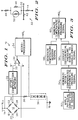
- FIG. 1 illustrates a schematic block diagram of a sensor circuit 10 suitable for manufacture as an integrated circuit using conventional integrated circuit processing techniques.
- Sensor circuit 10 includes a transducer 12 coupled between a power supply conductor 14 and a power supply conductor 16.
- transducer 12 is a piezo-resistive bridge network comprising piezo-resistive elements 18, 22, 26, and 28.
- piezo-resistors 18, 22, 26, and 28 are silicon resistors.
- Piezo-resistive element 18 is coupled between power supply conductor 14 and node 20.
- Piezo-resistive element 22 is coupled between power supply conductor 14 and node 24.
- Piezo-resistive element 26 is coupled between node 20 and power supply conductor 16 and piezo-resistive element 28 is coupled between node 24 and power supply conductor 16. It should be noted that the piezo-resistive elements are also referred to as piezo-resistors and that nodes 20 and 24 serve as transducer output nodes.
- a suitable operating range for power supply conductor 14 is from approximately 5 volts to approximately 24 volts and a suitable operating potential for power supply conductor 16 is ground potential. Power supply conductor 14 is also referred to as V CC .
- piezo-resistive elements 18, 22, 26, and 28 become unbalanced in response to an external physical condition such as, for example, an applied pressure, temperature, acceleration, etc.
- the physical condition deflects the semiconductor material from which piezo-resistive bridge 12 is formed, thereby increasing the resistance of one set of opposing bridge resistors, e.g., resistors 18 and 28, and decreasing the resistance of the other set of opposing bridge resistors, e.g., resistors 22 and 26.
- the resistance values of bridge resistors 18 and 28 increase by the same amount that the resistance values of bridge resistors 22 and 26 decrease.
- bridge resistors 18, 22, 26, and 28 are fabricated to have resistance values of 1,000 ohms in the absence of the physical condition. In the presence of the physical condition, bridge resistors 18 and 28 may increase to approximately 1,002 ohms, while bridge resistors 22 and 26 decrease to approximately 998 ohms, i.e., resistive bridge 12 is unbalanced. The unbalance creates a differential signal between output terminals S+ and S ⁇ that is applied to the non-inverting and inverting inputs, respectively, of differential amplifier 30.
- signal S+ appears at an output terminal 33 of a compensation network 32
- signal S ⁇ appears at node 20.
- node 24 is coupled to the non-inverting input terminal of differential amplifier 30 via offset compensation network 32
- node 20 is coupled directly to the inverting input terminal of operational amplifier 30.
- Offset compensation network 32 is used to compensate for the temperature coefficient of the offset as well as to null the nominal offset of the sensor. Offset compensation network 32 may be implemented as a network of resistors and thermistors as is well known in the art.
- FIG. 2 illustrates an example of an offset compensation network 32 suitable for use in sensor 10.
- offset compensation network 32 includes trimmable metal film resistors 42, 44, 46, and 48 and a thermistor 50.
- metal film resistors 42, 44, 46, and 48 are chrome silicon resistors and thermistor 50 is a polysilicon resistor.
- Resistor 42 has a first terminal which serves as an input terminal for offset compensation network 32 and a second terminal 33 which serves as the output terminal of offset compensation network 32.
- Resistor 44 has a first terminal for coupling with a power supply conductor, such as power supply conductor 16 of FIG.
- thermistor 50 is a p ⁇ silicon resistor having the same coefficient of thermal resistance as bridge network 12. Methods of forming trimmable metal-film resistors and thermistors are known to those skilled in the art.
- an output signal of differential amplifier 30 provides a sensor signal to a microprocessor 34. It should be understood that the sensor signal is uncompensated for variation due to the negative temperature coefficient of full-scale span.
- sensor 10 of the present invention includes a resistor 36 coupled in series to a temperature sensing circuit 38, wherein one terminal of resistor 36 is coupled to power supply conductor 14 and one terminal of temperature sensing circuit 38 is coupled to power supply conductor 16. More particularly, a first terminal of resistor 36 is connected to power supply conductor 14, a second terminal of resistor 36 is connected to a first terminal of temperature sensing circuit 38 and a second terminal of temperature sensing circuit 38 is connected to power supply conductor 16. In addition, the first terminal of temperature sensing circuit 38 is coupled to microprocessor 34 and provides a temperature sense voltage signal, V TEMP , to microprocessor 34.
- V TEMP temperature sense voltage signal
- Temperature sensing circuit 38 may be, for example, a diode, a series connected string of diodes, a thermistor, a band-gap reference circuit, and the like.
- temperature sensing circuit 38 comprises a series-connected string of four diodes.
- the temperature coefficient of a forward biased diode is approximately -2.26 millivolts (mV) per °C and the string of four series-connected diodes has a temperature coefficient of approximately -9 mV per °C.
- V TEMP the voltage signal
- the voltage signal V TEMP serves as a temperature sense signal which is input into microprocessor 34.
- An important feature of the present invention is that temperature sensing circuit 38 is monolithically integrated with bridge network 12, thereby providing a precise measure of the silicon die temperature in response to ambient temperature variations.
- FIG. 3 is a flow chart illustrating the process of compensating for temperature variation in accordance with an embodiment of the present invention.
- a physical condition e.g., pressure
- the differential voltage signal is compensated for offset in step 54, thereby generating an offset compensated differential sensor signal having a span of operation between a minimum state of the physical condition and a maximum state of the physical condition.
- an offset compensated differential sensor signal having a span of operation between a minimum pressure and a maximum pressure is generated.
- the offset compensated differential voltage signal is converted into a single-ended offset compensated voltage signal.
- a temperature sense signal is also being generated, i.e., step 58 of FIG. 3, by temperature sensing circuit 38 of FIG. 1.
- the temperature sense signal is used to compensate for variation in the span of operation of the offset compensated sensor signal due to temperature changes.
- a temperature compensated pressure signal S C is generated, step 60 of FIG. 3, in accordance with the temperature sense signal and the single-ended offset compensated signal.
- One technique for generating the temperature compensated pressure signal is to calibrate pressure sensor 10 at zero pressure differential and room temperature and then calibrate pressure sensor 10 at full-scale pressure at room temperature.
- pressure sensor 10 is calibrated at zero pressure differential and a temperature different than room temperature and then pressure sensor 10 is calibrated at full-scale pressure at the temperature different than room temperature.
- the temperature different than room temperature is room temperature plus twenty degrees Celsius.
- pressure sensor 10 is calibrated at 25 °C, i.e., room temperature, and 45 °C, i.e., room temperature plus 20 °C.
- the percent change in the offset compensated single-ended output signal over the twenty degree Celsius temperature range is calculated.
- a temperature compensation factor of sensor 10 is determined to be approximately -1,900 parts per million per °C (ppm/°C). In other words, as the temperature of sensor 10 increases, the span of sensor 10 decreases by approximately 1,900 ppm/°C.
- the offset compensated single-ended output signal is compensated for temperature changes by shifting it by +1,900 ppm/°C in accordance with the temperature sense signal from temperature sense circuit 38.
- a convenient means for shifting the single-ended output signal is to store the span of sensor 10 in microprocessor 34 (shown in FIG. 1) and input the temperature sense signal from temperature sense circuit 38 as well as the offset compensated single-ended output signal into microprocessor 34.
- microprocessor 34 uses the span of sensor 10 to provide an offset and temperature compensated output signal S C .
- amplifier 30 and microprocessor 34 serve as a means for compensating for variation in the span of operation of the offset compensated sensor signal due to temperature changes.
- microprocessor 34 is a Motorola microprocessor having part number MC68HC705P9.
- a key feature of the present invention is that the temperature sensing circuit is monolithically integrated with the bridge network, i.e., the transducer.
- the operating temperature of the silicon die is precisely determined and used, in conjunction with a temperature compensation factor, to compensate for temperature variations of the sensor output signal.
- the present invention eliminates the use of resistors for temperature compensating the full-scale span, thereby increasing the bias voltage across the bridge network and increasing the sensitivity of the bridge network. More particularly, the sensitivity of the bridge network, and thus the sensor, is improved when compared to a sensor having compensation resistors coupled between the power supply terminals and the bridge network because all of the supply voltage appears across the bridge network rather than across the compensation resistors.
Landscapes
- Physics & Mathematics (AREA)
- General Physics & Mathematics (AREA)
- Measuring Fluid Pressure (AREA)
- Measurement Of Force In General (AREA)
Applications Claiming Priority (2)
| Application Number | Priority Date | Filing Date | Title |
|---|---|---|---|
| US33220394A | 1994-10-31 | 1994-10-31 | |
| US332203 | 1994-10-31 |
Publications (1)
| Publication Number | Publication Date |
|---|---|
| EP0709660A1 true EP0709660A1 (de) | 1996-05-01 |
Family
ID=23297173
Family Applications (1)
| Application Number | Title | Priority Date | Filing Date |
|---|---|---|---|
| EP95116692A Withdrawn EP0709660A1 (de) | 1994-10-31 | 1995-10-23 | Sensor und Verfahren zur Temperaturkompensation der Bereichsvariation des Sensors |
Country Status (3)
| Country | Link |
|---|---|
| EP (1) | EP0709660A1 (de) |
| JP (1) | JPH08226862A (de) |
| NO (1) | NO953285L (de) |
Cited By (2)
| Publication number | Priority date | Publication date | Assignee | Title |
|---|---|---|---|---|
| CN113687124A (zh) * | 2020-05-19 | 2021-11-23 | 意法半导体股份有限公司 | 具有温度补偿的电阻桥传感器 |
| US11402275B2 (en) | 2016-08-05 | 2022-08-02 | Denso Corporation | Sensor apparatus |
Families Citing this family (3)
| Publication number | Priority date | Publication date | Assignee | Title |
|---|---|---|---|---|
| JPH11211586A (ja) * | 1998-01-27 | 1999-08-06 | Matsushita Electric Works Ltd | 半導体装置 |
| JP4578427B2 (ja) * | 2006-03-28 | 2010-11-10 | 株式会社豊田中央研究所 | 応力温度測定装置 |
| WO2013065152A1 (ja) * | 2011-11-02 | 2013-05-10 | パイオニア株式会社 | 検出装置、検出装置が取り付けられたクランク、検出装置が取り付けられた自転車、電圧値の補正方法、電圧値補正プログラム及び電圧値補正プログラムを記録した媒体 |
Citations (4)
| Publication number | Priority date | Publication date | Assignee | Title |
|---|---|---|---|---|
| US4468968A (en) * | 1983-04-21 | 1984-09-04 | The Singer Company | Method and arrangement for providing information to define the values of a set of parameters which characterize an element |
| EP0169414A2 (de) * | 1984-07-27 | 1986-01-29 | Keller AG für Druckmesstechnik | Verfahren zur Temperaturkompensation und Messschaltung hierfür |
| WO1988006719A1 (en) * | 1987-03-05 | 1988-09-07 | The Secretary Of State For Defence In Her Britanni | Transducer signal conditioner |
| US4986131A (en) * | 1988-12-28 | 1991-01-22 | Kabushiki Kaisha Toyota Chuo Kenkyusho | Semiconductor strain detector |
-
1995
- 1995-08-22 NO NO953285A patent/NO953285L/no not_active Application Discontinuation
- 1995-10-18 JP JP29383095A patent/JPH08226862A/ja active Pending
- 1995-10-23 EP EP95116692A patent/EP0709660A1/de not_active Withdrawn
Patent Citations (4)
| Publication number | Priority date | Publication date | Assignee | Title |
|---|---|---|---|---|
| US4468968A (en) * | 1983-04-21 | 1984-09-04 | The Singer Company | Method and arrangement for providing information to define the values of a set of parameters which characterize an element |
| EP0169414A2 (de) * | 1984-07-27 | 1986-01-29 | Keller AG für Druckmesstechnik | Verfahren zur Temperaturkompensation und Messschaltung hierfür |
| WO1988006719A1 (en) * | 1987-03-05 | 1988-09-07 | The Secretary Of State For Defence In Her Britanni | Transducer signal conditioner |
| US4986131A (en) * | 1988-12-28 | 1991-01-22 | Kabushiki Kaisha Toyota Chuo Kenkyusho | Semiconductor strain detector |
Cited By (2)
| Publication number | Priority date | Publication date | Assignee | Title |
|---|---|---|---|---|
| US11402275B2 (en) | 2016-08-05 | 2022-08-02 | Denso Corporation | Sensor apparatus |
| CN113687124A (zh) * | 2020-05-19 | 2021-11-23 | 意法半导体股份有限公司 | 具有温度补偿的电阻桥传感器 |
Also Published As
| Publication number | Publication date |
|---|---|
| JPH08226862A (ja) | 1996-09-03 |
| NO953285D0 (no) | 1995-08-22 |
| NO953285L (no) | 1996-05-02 |
Similar Documents
| Publication | Publication Date | Title |
|---|---|---|
| US5507171A (en) | Electronic circuit for a transducer | |
| EP0086462B1 (de) | Druckwandler mit Halbleiterdehnungsmessstreifen | |
| CA1135529A (en) | Semiconductor pressure detector apparatus with zero-point temperature compensation | |
| EP0409213B1 (de) | Verstärkungsschaltkreis mit Temperaturausgleich für Halbleiterdruckwandler | |
| US4233848A (en) | Strain gauge pressure transducer apparatus having an improved impedance bridge | |
| US5795069A (en) | Temperature sensor and method | |
| US3967188A (en) | Temperature compensation circuit for sensor of physical variables such as temperature and pressure | |
| US5187985A (en) | Amplified pressure transducer | |
| US4798093A (en) | Apparatus for sensor compensation | |
| US5686826A (en) | Ambient temperature compensation for semiconductor transducer structures | |
| US5241850A (en) | Sensor with programmable temperature compensation | |
| CN1122631A (zh) | 具有完整温度信号的应变仪传感器 | |
| EP3627699B1 (de) | Verstärker mit gleichtaktdetektion | |
| US5796291A (en) | Method and apparatus for compensating for temperature fluctuations in the input to a gain circuit | |
| WO1988006719A1 (en) | Transducer signal conditioner | |
| US6011422A (en) | Integrated differential voltage amplifier with programmable gain and input offset voltage | |
| JPH0972805A (ja) | 半導体センサ | |
| US6107861A (en) | Circuit for self compensation of silicon strain gauge pressure transmitters | |
| JPH08226862A (ja) | センサおよび該センサにおける測定範囲変動を温度補償する方法 | |
| JPH11160347A (ja) | センサ回路 | |
| JPH10339680A (ja) | 半導体圧力センサ | |
| KR100238390B1 (ko) | 압력센서의 온도 보상 회로 | |
| RU2165602C2 (ru) | Полупроводниковый датчик давления | |
| JPH0545130B2 (de) | ||
| JPH032640A (ja) | 半導体圧力センサーの温度補償回路 |
Legal Events
| Date | Code | Title | Description |
|---|---|---|---|
| PUAI | Public reference made under article 153(3) epc to a published international application that has entered the european phase |
Free format text: ORIGINAL CODE: 0009012 |
|
| AK | Designated contracting states |
Kind code of ref document: A1 Designated state(s): DE FR GB |
|
| 17P | Request for examination filed |
Effective date: 19961104 |
|
| 17Q | First examination report despatched |
Effective date: 19971201 |
|
| GRAG | Despatch of communication of intention to grant |
Free format text: ORIGINAL CODE: EPIDOS AGRA |
|
| STAA | Information on the status of an ep patent application or granted ep patent |
Free format text: STATUS: THE APPLICATION IS DEEMED TO BE WITHDRAWN |
|
| 18D | Application deemed to be withdrawn |
Effective date: 19990501 |