EP0709715A2 - Dispositif d'affichage en couleurs à cristal liquide - Google Patents
Dispositif d'affichage en couleurs à cristal liquide Download PDFInfo
- Publication number
- EP0709715A2 EP0709715A2 EP95115731A EP95115731A EP0709715A2 EP 0709715 A2 EP0709715 A2 EP 0709715A2 EP 95115731 A EP95115731 A EP 95115731A EP 95115731 A EP95115731 A EP 95115731A EP 0709715 A2 EP0709715 A2 EP 0709715A2
- Authority
- EP
- European Patent Office
- Prior art keywords
- display area
- colored
- light
- liquid crystal
- substrate
- Prior art date
- Legal status (The legal status is an assumption and is not a legal conclusion. Google has not performed a legal analysis and makes no representation as to the accuracy of the status listed.)
- Granted
Links
- 239000004973 liquid crystal related substance Substances 0.000 title claims abstract description 51
- 239000000758 substrate Substances 0.000 claims abstract description 63
- 239000011347 resin Substances 0.000 claims description 9
- 229920005989 resin Polymers 0.000 claims description 9
- 239000000463 material Substances 0.000 claims description 5
- 239000000049 pigment Substances 0.000 claims description 5
- 229920002120 photoresistant polymer Polymers 0.000 description 6
- 239000007788 liquid Substances 0.000 description 3
- 238000004519 manufacturing process Methods 0.000 description 3
- VYZAMTAEIAYCRO-UHFFFAOYSA-N Chromium Chemical compound [Cr] VYZAMTAEIAYCRO-UHFFFAOYSA-N 0.000 description 2
- 229910021417 amorphous silicon Inorganic materials 0.000 description 2
- 230000015572 biosynthetic process Effects 0.000 description 2
- 229910052804 chromium Inorganic materials 0.000 description 2
- 239000011651 chromium Substances 0.000 description 2
- 239000003086 colorant Substances 0.000 description 2
- 229910052751 metal Inorganic materials 0.000 description 2
- 239000002184 metal Substances 0.000 description 2
- 230000002087 whitening effect Effects 0.000 description 2
- 239000011159 matrix material Substances 0.000 description 1
Images

Classifications
-
- G—PHYSICS
- G02—OPTICS
- G02F—OPTICAL DEVICES OR ARRANGEMENTS FOR THE CONTROL OF LIGHT BY MODIFICATION OF THE OPTICAL PROPERTIES OF THE MEDIA OF THE ELEMENTS INVOLVED THEREIN; NON-LINEAR OPTICS; FREQUENCY-CHANGING OF LIGHT; OPTICAL LOGIC ELEMENTS; OPTICAL ANALOGUE/DIGITAL CONVERTERS
- G02F1/00—Devices or arrangements for the control of the intensity, colour, phase, polarisation or direction of light arriving from an independent light source, e.g. switching, gating or modulating; Non-linear optics
- G02F1/01—Devices or arrangements for the control of the intensity, colour, phase, polarisation or direction of light arriving from an independent light source, e.g. switching, gating or modulating; Non-linear optics for the control of the intensity, phase, polarisation or colour
- G02F1/13—Devices or arrangements for the control of the intensity, colour, phase, polarisation or direction of light arriving from an independent light source, e.g. switching, gating or modulating; Non-linear optics for the control of the intensity, phase, polarisation or colour based on liquid crystals, e.g. single liquid crystal display cells
- G02F1/133—Constructional arrangements; Operation of liquid crystal cells; Circuit arrangements
- G02F1/1333—Constructional arrangements; Manufacturing methods
- G02F1/1335—Structural association of cells with optical devices, e.g. polarisers or reflectors
- G02F1/133509—Filters, e.g. light shielding masks
- G02F1/133512—Light shielding layers, e.g. black matrix
-
- G—PHYSICS
- G02—OPTICS
- G02F—OPTICAL DEVICES OR ARRANGEMENTS FOR THE CONTROL OF LIGHT BY MODIFICATION OF THE OPTICAL PROPERTIES OF THE MEDIA OF THE ELEMENTS INVOLVED THEREIN; NON-LINEAR OPTICS; FREQUENCY-CHANGING OF LIGHT; OPTICAL LOGIC ELEMENTS; OPTICAL ANALOGUE/DIGITAL CONVERTERS
- G02F1/00—Devices or arrangements for the control of the intensity, colour, phase, polarisation or direction of light arriving from an independent light source, e.g. switching, gating or modulating; Non-linear optics
- G02F1/01—Devices or arrangements for the control of the intensity, colour, phase, polarisation or direction of light arriving from an independent light source, e.g. switching, gating or modulating; Non-linear optics for the control of the intensity, phase, polarisation or colour
- G02F1/13—Devices or arrangements for the control of the intensity, colour, phase, polarisation or direction of light arriving from an independent light source, e.g. switching, gating or modulating; Non-linear optics for the control of the intensity, phase, polarisation or colour based on liquid crystals, e.g. single liquid crystal display cells
- G02F1/133—Constructional arrangements; Operation of liquid crystal cells; Circuit arrangements
- G02F1/1333—Constructional arrangements; Manufacturing methods
- G02F1/1335—Structural association of cells with optical devices, e.g. polarisers or reflectors
- G02F1/133509—Filters, e.g. light shielding masks
- G02F1/133514—Colour filters
-
- G—PHYSICS
- G02—OPTICS
- G02F—OPTICAL DEVICES OR ARRANGEMENTS FOR THE CONTROL OF LIGHT BY MODIFICATION OF THE OPTICAL PROPERTIES OF THE MEDIA OF THE ELEMENTS INVOLVED THEREIN; NON-LINEAR OPTICS; FREQUENCY-CHANGING OF LIGHT; OPTICAL LOGIC ELEMENTS; OPTICAL ANALOGUE/DIGITAL CONVERTERS
- G02F1/00—Devices or arrangements for the control of the intensity, colour, phase, polarisation or direction of light arriving from an independent light source, e.g. switching, gating or modulating; Non-linear optics
- G02F1/01—Devices or arrangements for the control of the intensity, colour, phase, polarisation or direction of light arriving from an independent light source, e.g. switching, gating or modulating; Non-linear optics for the control of the intensity, phase, polarisation or colour
- G02F1/13—Devices or arrangements for the control of the intensity, colour, phase, polarisation or direction of light arriving from an independent light source, e.g. switching, gating or modulating; Non-linear optics for the control of the intensity, phase, polarisation or colour based on liquid crystals, e.g. single liquid crystal display cells
- G02F1/133—Constructional arrangements; Operation of liquid crystal cells; Circuit arrangements
- G02F1/136—Liquid crystal cells structurally associated with a semi-conducting layer or substrate, e.g. cells forming part of an integrated circuit
- G02F1/1362—Active matrix addressed cells
Definitions
- the invention relates to a color liquid display, and more particularly to an active matrix color liquid display including two transparent substrates facing to each other, on one of which are arranged switching elements in an array configuration.
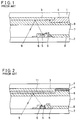
- Fig. 1 is a cross-sectional view illustrating an outermost end of a display area of a conventional color liquid crystal display (LCD).
- LCD liquid crystal display
- a pair of transparent substrates 1 and 2 are disposed in facing relation.
- a light-impermeable layer 3 composed of metal such as chromium, a colored layer 4 a part of which overlies on the light-impermeable layer 3 and the remainder of which directly overlies on the substrate 1, and a transparent electrode 8 entirely covering over the light-impermeable layer 3 and the colored layer 4.
- a plurality of picture element switching elements 5 composed of, for instance, a thin amorphous silicon film, a pair of picture element wirings 6 which are disposed adjacent to and at opposite sides of the switching element 5 and a part of which overlies on the switching element 5, and a transparent electrode 8 a part of which overlies on one of the picture element wirings 6 and which extends in the same direction as a direction in which the colored layer 4 extends.
- a liquid crystal layer 7 As illustrated in Fig. 1, the colored layer 4 generally overlaps the light-impermeable layer 3 to the extent that an end of the colored layer 4 reaches an end of the switching element 5 disposed on the transparent substrate 2.
- Fig. 2 illustrates another conventional color liquid crystal display having been suggested in Japanese Unexamined Patent Public Disclosures Nos. 4-1726 and 4-1728.
- this color liquid crystal display on the light-impermeable layer 3 is further formed a film 11 which absorbs a light thereinto in No. 4-1726 or a thin resin film 11 in No. 4-1728.
- the light-impermeable layer 3 has a function of preventing a light transmitting through the transparent substrate 1 and directing towards the transparent substrate 2 from being radiated to the switching element 5.
- a light reflected from the light-impermeable layer 3 is radiated to the switching element 5 at its end, thereby a backward current generating in the switching element 5.
- the backward current causes the black level at an end of a display to be whitened.
- the liquid crystal display having the light-absorbing film or thin resin film 11 overlying the light-impermeable layer 3 as illustrated in Fig. 2 can almost overcome the above mentioned problem.
- photo resist is used in the formation of the colored layer 4.
- a step tends to be unadvantageously formed on a surface of the colored layer 4 at its end, since exposure condition delicately changes due to a light transmitting from the outside of a photo resist mask. If a colored layer having a step thereon is used as a display, there arises a problem of display nonuniformity, because the stepped portion has a different transmissivity from other portions.
- the invention provides a color liquid crystal display comprising: (a) two transparent substrates A and B disposed in facing relation; (b) a plurality of switching elements disposed on a surface of the substrate A, the surface facing the substrate B, the switching elements defining an area; (c) a light-impermeable layer disposed on a surface of the substrate B, the surface facing the substrate A; and (d) a colored layer overlying the light-impermeable layer and defining a display area corresponding to the area defined by the switching elements, the color liquid crystal display being characterized in that the colored layer has an extension extending over the display area in longitudinal and transverse directions of the display area.
- the invention further provides a color liquid crystal display comprising: (a) two transparent substrates A and B disposed in facing relation; (b) a plurality of switching elements disposed on a surface of the substrate A, the surface facing the substrate B, the switching elements defining an area; (c) a light-impermeable layer disposed on a surface of the substrate B, the surface facing the substrate A; and (d) a colored layer overlying the light-impermeable layer and defining a display area corresponding to the area defined by the switching elements, the color liquid crystal display being characterized in that the colored layer comprises a red-colored stripe-shaped region, a green-colored stripe-shaped region and a blue-colored stripe-shaped region successively arranged adjacent to each other in a longitudinal direction of the display area, each of the regions comprising a plurality of picture elements successively arranged adjacent to each other in a transverse direction of the display area, and that the colored layer has extensions extending over the display area in the longitudinal and transverse directions of the display area, the
- the invention still further provides a color liquid crystal display comprising: (a) two transparent substrates A and B disposed in facing relation; (b) a plurality of switching elements disposed on a surface of the substrate A, the surface facing the substrate B, the switching elements defining an area; (c) a light-impermeable layer disposed on a surface of the substrate B, the surface facing the substrate A; and (d) a colored layer overlying the light-impermeable layer and defining a display area corresponding to the area defined by the switching elements, the color liquid crystal display being characterized in that the colored layer comprises red-colored picture elements, green-colored picture elements and blue-colored picture elements successively arranged adjacent to each other in a lattice configuration in longitudinal and transverse directions of the display area so that one of the picture elements is surrounded by the other two picture elements, and that the colored layer has extensions extending over the display area in the longitudinal and transverse directions of the display area, the longitudinal extension having a length of at least three picture elements and the transverse extension (10c, 10
- the invention yet further provides a color liquid crystal display comprising: (a) two transparent substrates A and B disposed in facing relation; (b) a plurality of switching elements disposed on a surface of the substrate A, the surface facing the substrate B, the switching elements defining an area; (c) a light-impermeable layer disposed on a surface of the substrate B, the surface facing the substrate A; and (d) a colored layer overlying the light-impermeable layer and defining a display area corresponding to the area defined by the switching elements, the color liquid crystal display being characterized in that the colored layer comprises a plurality of rows each comprising red-colored picture elements, green-colored picture elements and blue-colored picture elements successively arranged adjacent to each other in a longitudinal direction in the display area, the rows being offset to each other by half of a length of one picture element so that one of the picture elements is surrounded by the other two picture elements, and that the colored layer has extensions extending over the display area in the longitudinal and transverse directions of the display area, the longitudinal extension having
- the light-impermeable layer By covering the light-impermeable layer with the extensions of the colored layer, it is possible to absorb a back light in the colored layer. The remainder light not absorbed in the colored layer and thus having transmitted therethrough is reflected at the light-impermeable layer. It is also possible to absorb the thus reflected light in the colored layer.
- the black level in the display area can be prevented from being whitened. According to the experiment which the inventors had conducted, whitening of the black level of the display area at the end thereof could be completely prevented.
- the extensions of the colored layer can be formed only by modifying a photo resist pattern.
- the display area constituted of the colored layer originates from a colored layer disposed at least second outermost, and hence it is no longer necessary to use an outermost colored layer which has a step thereon. Accordingly, nonuniformity of display to be caused by a stepped portion of a colored layer can be prevented.
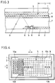
- Fig. 3 illustrates an end portion of a display area of a color liquid crystal display in accordance with the first embodiment of the present invention.
- the liquid crystal display has two transparent substrates 1 and 2 disposed in facing relation.
- a light-impermeable layer 3 composed of metal such as chromium, a colored layer 4 a part of which overlies on the light-impermeable layer 3 and the remainder of which directly overlies on the substrate 1, and a transparent electrode 8 entirely covering over the colored layer 4.
- a plurality of picture element switching elements 5 (only one is illustrated) composed of, for instance, a thin amorphous silicon film, a pair of picture element wirings 6 which are disposed adjacent to and at opposite sides of the switching element 5 and a part of which overlies on the switching element 5, and a transparent electrode 8 a part of which overlies on one of the picture element wirings 6 and which extends in one direction.
- a liquid crystal layer 7 Between the substrates 1 and 2 are enclosed liquid crystal to thereby form a liquid crystal layer 7.
- the plurality of switching elements 5 define a certain area, and the colored layer 4 also defines a display area S corresponding to the area defined by the switching elements 5.
- the colored layer 4 is formed with extensions 10a, 10b, 10c and 10d (see Fig. 4) each of which extends outwardly by a length of at least one picture element from a position which the switching element 5 faces.
- the extensions are made of the same material as that of the colored layer 4 constituting the display area S.
- the colored layer 4 is made of light-permeable resin containing pigment therein.
- a back light 9 having transmitted through the transparent substrate 2 is absorbed in the colored layer 4.
- the remainder light not absorbed in the colored layer 4 is reflected at the light-impermeable layer 3.
- the thus reflected light can be absorbed in the colored layer 4, and hence it is possible to reduce a light reflected from the light-impermeable layer 3 and radiated to the switching element 5 disposed at the end of the display area S. As a result, it is possible to prevent the black level at the boundary of the display area, which is caused by a backward current running through the switching element 5, from being whitened.
- Fig. 4 is a plan view of the substrate 1 on which the colored layer 4 is arranged in a pattern.
- the colored layer 4 consists of a plurality of stripes.
- the colored layer 4 means one disposed within the display area S.
- the colored layer 4 comprises a red-colored stripe-shaped region R, a green-colored stripe-shaped region G and a blue-colored stripe-shaped region B successively arranged adjacent to each other in a longitudinal direction L of the display area S.
- Each of the regions R, G and B comprises a plurality of picture elements successively arranged adjacent to each other in a transverse direction T of the display area S.
- the colored layer 4 is formed with the extensions 10a, 10b, 10c and 10d extending over the display area S.
- the extensions 10a and 10b extend over the display S in the longitudinal direction L of the display area S, while the extensions 10c and 10d extend in the transverse direction T of the display area S.
- Each of the longitudinal extensions 10a and 10b has a length of three picture elements, while each of the transverse extensions 10c and 10d has a length of one picture element.
- extensions 10a to 10d may have a greater length.
- the longitudinal extensions 10a and 10b may have a length of four picture elements or greater, while the transverse extensions 10c and 10d may have a length of two picture elements or greater.
- the invention merely extends the colored layer 4 to form the extensions 10a to 10d, and hence does not need to newly add fabrication steps.
- photo resist is used for forming each of the colored regions R, G and B in the formation of the colored layer 4, the arrangement of the colored layer 4 as illustrated in Fig. 4 can be obtained only by enlarging a photo resist pattern above and below the display area S by a length of one picture element and to the left and right of the display area S by a length of three picture elements.
- the three picture elements to be included in each of the extensions 10a and 10b are red-colored, green-colored and blue-colored picture elements.
- the conventional color liquid display shows the nonuniformity of display to be caused by a step formed on the colored layer, by about 7%.
- the invention can reduce the display nonuniformity down to 1% or less.
- Fig. 5 shows an arrangement of picture elements in the colored layer 4 of the color liquid crystal display in accordance with the second embodiment of the present invention.
- the arrangement of picture elements illustrated in Fig. 5 is generally called mosaic type.
- the colored layer 4 comprises red-colored picture elements R, green-colored picture elements G and blue-colored picture elements B successively arranged in a lattice configuration. Namely, the picture elements R, G and B are disposed adjacent to each other in longitudinal and transverse directions of the display area S. In addition, the picture elements are disposed so that one of the picture elements is surrounded by the other two picture elements. For instance, the red-colored picture element R is surrounded only by the green-colored and blue-colored picture elements G and B, and never surrounded by the red-colored picture element R.
- the colored layer 4 has extensions 10a, 10b, 10c and 10d extending over the display area S in both the longitudinal and transverse directions L and T of the display area S.
- each of the longitudinal extensions 10a and 10b has a length of three picture elements
- each of the transverse extensions 10c and 10d also has a length of three picture elements.
- the color liquid crystal display in accordance with the second embodiment has the same cross-section as that of the first embodiment illustrated in Fig. 3.
- a light to be radiated to the switching element 5 disposed on the substrate 2 can be reduced, and hence the whitening of the black level at the outermost region of the display area S can be prevented.
- the difference of the second embodiment from the first embodiment is that a picture element having one of the three colors is surrounded by picture elements having the other two colors.
- the extensions 10a to 10d may have a greater length.
- the longitudinal and transverse extensions 10a to 10d may have a length of four picture elements or greater.
- the extensions 10a to 10d having a length of three picture elements can be formed without additional fabrication steps, similarly to the first embodiment. Namely, the extensions 10a to 10d can be formed only by changing a photo resist pattern.
- Fig. 6 shows an arrangement of picture elements in the colored layer 4 of the color liquid crystal display in accordance with the third embodiment of the present invention.
- the arrangement of picture elements illustrated in Fig. 6 is generally called triangular type.
- the colored layer 4 comprises a plurality of rows 12a to 12n.
- Each of the rows 12a to 12n comprises red-colored picture elements, green-colored picture elements and blue-colored picture elements successively arranged adjacent to each other in a longitudinal direction L of the color liquid crystal display.
- the picture element rows 12a to 12n are offset to each other by half of a length of one picture element so that one of the picture elements is surrounded by the other two picture elements. For instance, the red-colored picture element R is surrounded only by the green-colored and blue-colored picture elements G and B, and never surrounded by the red-colored picture element R.
- the colored layer 4 has extensions 10a, 10b, 10c and 10d extending over the display area S in both the longitudinal and transverse directions of the display area S.
- Each of the longitudinal extensions 10a and 10b has a length of three picture elements
- each of the transverse extensions 10c and 10d has a length of three picture elements.
- the transverse extension 10c comprises the rows 12a to 12c
- the transverse extension 10d comprises the rows 12(n-2) to 12n.
- the color liquid crystal display in accordance with the third embodiment has the same structure as that of the first and second embodiments except the above mentioned arrangement of the picture elements R, G and B, and hence has the same operation and function as those of the first and second embodiments.
Landscapes
- Physics & Mathematics (AREA)
- Nonlinear Science (AREA)
- Mathematical Physics (AREA)
- Chemical & Material Sciences (AREA)
- Crystallography & Structural Chemistry (AREA)
- General Physics & Mathematics (AREA)
- Optics & Photonics (AREA)
- Liquid Crystal (AREA)
- Devices For Indicating Variable Information By Combining Individual Elements (AREA)
Applications Claiming Priority (3)
| Application Number | Priority Date | Filing Date | Title |
|---|---|---|---|
| JP265572/94 | 1994-10-28 | ||
| JP26557294 | 1994-10-28 | ||
| JP26557294A JPH08122767A (ja) | 1994-10-28 | 1994-10-28 | カラー液晶ディスプレイ |
Publications (3)
| Publication Number | Publication Date |
|---|---|
| EP0709715A2 true EP0709715A2 (fr) | 1996-05-01 |
| EP0709715A3 EP0709715A3 (fr) | 1997-03-19 |
| EP0709715B1 EP0709715B1 (fr) | 2004-03-31 |
Family
ID=17418983
Family Applications (1)
| Application Number | Title | Priority Date | Filing Date |
|---|---|---|---|
| EP95115731A Expired - Lifetime EP0709715B1 (fr) | 1994-10-28 | 1995-10-05 | Dispositif d'affichage en couleurs à cristal liquide |
Country Status (5)
| Country | Link |
|---|---|
| US (1) | US5812228A (fr) |
| EP (1) | EP0709715B1 (fr) |
| JP (1) | JPH08122767A (fr) |
| DE (1) | DE69532792T2 (fr) |
| TW (1) | TW346548B (fr) |
Cited By (1)
| Publication number | Priority date | Publication date | Assignee | Title |
|---|---|---|---|---|
| US5812228A (en) * | 1994-10-28 | 1998-09-22 | Nec Corporation | Color liquid crystal display with extensions of the colored layer cover the light-impermeable layer |
Families Citing this family (2)
| Publication number | Priority date | Publication date | Assignee | Title |
|---|---|---|---|---|
| DE69810408T2 (de) * | 1997-09-17 | 2003-09-25 | Matsushita Electric Ind Co Ltd | Reflektive Flüssigkristall-Anzeigevorrichtung |
| KR20010032543A (ko) * | 1997-11-28 | 2001-04-25 | 모리시타 요이찌 | 반사형 표시소자 및 반사형 표시소자를 이용한 영상장치 |
Citations (2)
| Publication number | Priority date | Publication date | Assignee | Title |
|---|---|---|---|---|
| JPH041726A (ja) | 1990-04-19 | 1992-01-07 | Matsushita Electric Ind Co Ltd | 液晶表示装置 |
| JPH041728A (ja) | 1990-04-19 | 1992-01-07 | Matsushita Electric Ind Co Ltd | 液晶表示装置 |
Family Cites Families (13)
| Publication number | Priority date | Publication date | Assignee | Title |
|---|---|---|---|---|
| JPS60218626A (ja) * | 1984-04-13 | 1985-11-01 | Sharp Corp | カラ−液晶表示装置 |
| JPS6455582A (en) * | 1987-08-06 | 1989-03-02 | Ibm | Color display device |
| EP0338412B2 (fr) * | 1988-04-21 | 2000-05-10 | Asahi Glass Company Ltd. | Dispositif d'affichage à cristal liquide en couleur et son procédé de commande |
| JPH0223412A (ja) * | 1988-07-13 | 1990-01-25 | Fujitsu Ltd | キーマトリックススイッチ装置 |
| US5402254B1 (en) * | 1990-10-17 | 1998-09-22 | Hitachi Ltd | Liquid crystal display device with tfts in which pixel electrodes are formed in the same plane as the gate electrodes with anodized oxide films before the deposition of silicon |
| JP3205373B2 (ja) * | 1992-03-12 | 2001-09-04 | 株式会社日立製作所 | 液晶表示装置 |
| JP3136200B2 (ja) * | 1992-07-22 | 2001-02-19 | 株式会社日立製作所 | 液晶表示装置 |
| US5311337A (en) * | 1992-09-23 | 1994-05-10 | Honeywell Inc. | Color mosaic matrix display having expanded or reduced hexagonal dot pattern |
| JPH06130217A (ja) * | 1992-10-20 | 1994-05-13 | Toshiba Corp | カラ−フィルタ及びその製造方法 |
| JPH06174916A (ja) * | 1992-12-08 | 1994-06-24 | Toshiba Corp | カラ−フィルタおよびその製造方法 |
| JP3210791B2 (ja) * | 1993-11-30 | 2001-09-17 | 京セラ株式会社 | カラー液晶表示装置の製造方法 |
| CA2157914C (fr) * | 1994-01-10 | 2008-04-22 | Richard I. Mccartney | Procede de fabrication d'affichages a cristaux liquides a domaines multiples |
| JPH08122767A (ja) * | 1994-10-28 | 1996-05-17 | Nec Kagoshima Ltd | カラー液晶ディスプレイ |
-
1994
- 1994-10-28 JP JP26557294A patent/JPH08122767A/ja active Pending
-
1995
- 1995-10-03 US US08/538,211 patent/US5812228A/en not_active Expired - Lifetime
- 1995-10-04 TW TW084110410A patent/TW346548B/zh not_active IP Right Cessation
- 1995-10-05 EP EP95115731A patent/EP0709715B1/fr not_active Expired - Lifetime
- 1995-10-05 DE DE1995632792 patent/DE69532792T2/de not_active Expired - Lifetime
Patent Citations (2)
| Publication number | Priority date | Publication date | Assignee | Title |
|---|---|---|---|---|
| JPH041726A (ja) | 1990-04-19 | 1992-01-07 | Matsushita Electric Ind Co Ltd | 液晶表示装置 |
| JPH041728A (ja) | 1990-04-19 | 1992-01-07 | Matsushita Electric Ind Co Ltd | 液晶表示装置 |
Cited By (1)
| Publication number | Priority date | Publication date | Assignee | Title |
|---|---|---|---|---|
| US5812228A (en) * | 1994-10-28 | 1998-09-22 | Nec Corporation | Color liquid crystal display with extensions of the colored layer cover the light-impermeable layer |
Also Published As
| Publication number | Publication date |
|---|---|
| DE69532792T2 (de) | 2005-01-13 |
| DE69532792D1 (de) | 2004-05-06 |
| EP0709715A3 (fr) | 1997-03-19 |
| TW346548B (en) | 1998-12-01 |
| JPH08122767A (ja) | 1996-05-17 |
| US5812228A (en) | 1998-09-22 |
| EP0709715B1 (fr) | 2004-03-31 |
Similar Documents
| Publication | Publication Date | Title |
|---|---|---|
| US5844645A (en) | Color liquid-crystal display device | |
| US7903211B2 (en) | Liquid crystal display having reflection electrodes | |
| US7142269B2 (en) | Color liquid crystal panel having opening in color filter varied according to color, method for manufacturing the same, and color liquid crystal display device employing the same | |
| US6323920B1 (en) | Methods of making LCD devices having color filter | |
| JP3296719B2 (ja) | カラー液晶表示素子及び該カラー液晶表示素子の製造方法 | |
| GB2259392A (en) | Liquid crystal display | |
| JP2004310057A (ja) | 反射透過型の液晶表示装置 | |
| JP2806741B2 (ja) | カラー液晶ディスプレイ | |
| JP4342277B2 (ja) | カラーフィルタ基板の製造方法、カラーフィルタ基板および表示装置 | |
| JP3329206B2 (ja) | カラー液晶表示装置および画素配列方法 | |
| US5812228A (en) | Color liquid crystal display with extensions of the colored layer cover the light-impermeable layer | |
| JPH09113890A (ja) | 液晶表示装置 | |
| EP1312973A2 (fr) | Dispositif d'affichage à cristaux liquides transflectif coloré et méthode de fabrication d'un substrat pour un tel dispositif | |
| CN222462281U (zh) | 显示面板及显示装置 | |
| JP3776184B2 (ja) | 液晶表示パネル | |
| JP3469732B2 (ja) | 液晶表示装置 | |
| JPS59159131A (ja) | 液晶表示装置 | |
| JPH0812353B2 (ja) | 液晶表示装置の製造方法 | |
| JPH07253587A (ja) | カラー液晶表示素子用電極基板 | |
| EP1469340B1 (fr) | Procede de formation d'une electrode de reflexion et d'un afficheur a cristaux liquides | |
| KR100671523B1 (ko) | 컬러 필터 기판 및 그의 제조 방법 | |
| KR100225144B1 (ko) | 칼라 액정 디스플레이 | |
| KR100552279B1 (ko) | 컬러 필터 기판 | |
| JP2008076724A (ja) | カラーフィルタ用フォトマスク、カラーフィルタの製造方法、カラーフィルタ、及び液晶表示装置 | |
| JPH03125120A (ja) | カラー液晶表示素子 |
Legal Events
| Date | Code | Title | Description |
|---|---|---|---|
| PUAI | Public reference made under article 153(3) epc to a published international application that has entered the european phase |
Free format text: ORIGINAL CODE: 0009012 |
|
| AK | Designated contracting states |
Kind code of ref document: A2 Designated state(s): DE GB NL |
|
| PUAL | Search report despatched |
Free format text: ORIGINAL CODE: 0009013 |
|
| AK | Designated contracting states |
Kind code of ref document: A3 Designated state(s): DE GB NL |
|
| 17P | Request for examination filed |
Effective date: 19970204 |
|
| 17Q | First examination report despatched |
Effective date: 20020417 |
|
| GRAP | Despatch of communication of intention to grant a patent |
Free format text: ORIGINAL CODE: EPIDOSNIGR1 |
|
| RAP1 | Party data changed (applicant data changed or rights of an application transferred) |
Owner name: NEC LCD TECHNOLOGIES, LTD. |
|
| GRAS | Grant fee paid |
Free format text: ORIGINAL CODE: EPIDOSNIGR3 |
|
| GRAA | (expected) grant |
Free format text: ORIGINAL CODE: 0009210 |
|
| AK | Designated contracting states |
Kind code of ref document: B1 Designated state(s): DE GB NL |
|
| REG | Reference to a national code |
Ref country code: GB Ref legal event code: FG4D |
|
| REF | Corresponds to: |
Ref document number: 69532792 Country of ref document: DE Date of ref document: 20040506 Kind code of ref document: P |
|
| PLBE | No opposition filed within time limit |
Free format text: ORIGINAL CODE: 0009261 |
|
| STAA | Information on the status of an ep patent application or granted ep patent |
Free format text: STATUS: NO OPPOSITION FILED WITHIN TIME LIMIT |
|
| 26N | No opposition filed |
Effective date: 20050104 |
|
| REG | Reference to a national code |
Ref country code: NL Ref legal event code: SD Effective date: 20100310 |
|
| REG | Reference to a national code |
Ref country code: GB Ref legal event code: 732E Free format text: REGISTERED BETWEEN 20100325 AND 20100331 |
|
| REG | Reference to a national code |
Ref country code: DE Ref legal event code: R082 Ref document number: 69532792 Country of ref document: DE Representative=s name: MURGITROYD & COMPANY, DE |
|
| REG | Reference to a national code |
Ref country code: NL Ref legal event code: SD Effective date: 20130329 |
|
| REG | Reference to a national code |
Ref country code: DE Ref legal event code: R082 Ref document number: 69532792 Country of ref document: DE Representative=s name: MURGITROYD & COMPANY, DE Effective date: 20130305 Ref country code: DE Ref legal event code: R082 Ref document number: 69532792 Country of ref document: DE Representative=s name: MURGITROYD & COMPANY, DE Effective date: 20130321 Ref country code: DE Ref legal event code: R081 Ref document number: 69532792 Country of ref document: DE Owner name: GOLD CHARM LIMITED, WS Free format text: FORMER OWNER: NEC CORP., TOKYO, JP Effective date: 20130305 |
|
| PGFP | Annual fee paid to national office [announced via postgrant information from national office to epo] |
Ref country code: GB Payment date: 20141001 Year of fee payment: 20 Ref country code: DE Payment date: 20140930 Year of fee payment: 20 |
|
| PGFP | Annual fee paid to national office [announced via postgrant information from national office to epo] |
Ref country code: NL Payment date: 20140926 Year of fee payment: 20 |
|
| REG | Reference to a national code |
Ref country code: DE Ref legal event code: R071 Ref document number: 69532792 Country of ref document: DE |
|
| REG | Reference to a national code |
Ref country code: NL Ref legal event code: MK Effective date: 20151004 |
|
| REG | Reference to a national code |
Ref country code: GB Ref legal event code: PE20 Expiry date: 20151004 |
|
| PG25 | Lapsed in a contracting state [announced via postgrant information from national office to epo] |
Ref country code: GB Free format text: LAPSE BECAUSE OF EXPIRATION OF PROTECTION Effective date: 20151004 |