EP0709892A2 - Verfahren zur Ausgestaltung von MOS-Invertern - Google Patents
Verfahren zur Ausgestaltung von MOS-Invertern Download PDFInfo
- Publication number
- EP0709892A2 EP0709892A2 EP95115447A EP95115447A EP0709892A2 EP 0709892 A2 EP0709892 A2 EP 0709892A2 EP 95115447 A EP95115447 A EP 95115447A EP 95115447 A EP95115447 A EP 95115447A EP 0709892 A2 EP0709892 A2 EP 0709892A2
- Authority
- EP
- European Patent Office
- Prior art keywords
- mos
- input
- inverters
- output
- inverter
- Prior art date
- Legal status (The legal status is an assumption and is not a legal conclusion. Google has not performed a legal analysis and makes no representation as to the accuracy of the status listed.)
- Granted
Links
Images


Classifications
-
- H—ELECTRICITY
- H10—SEMICONDUCTOR DEVICES; ELECTRIC SOLID-STATE DEVICES NOT OTHERWISE PROVIDED FOR
- H10D—INORGANIC ELECTRIC SEMICONDUCTOR DEVICES
- H10D84/00—Integrated devices formed in or on semiconductor substrates that comprise only semiconducting layers, e.g. on Si wafers or on GaAs-on-Si wafers
- H10D84/40—Integrated devices formed in or on semiconductor substrates that comprise only semiconducting layers, e.g. on Si wafers or on GaAs-on-Si wafers characterised by the integration of at least one component covered by groups H10D12/00 or H10D30/00 with at least one component covered by groups H10D10/00 or H10D18/00, e.g. integration of IGFETs with BJTs
- H10D84/401—Combinations of FETs or IGBTs with BJTs
-
- H—ELECTRICITY
- H03—ELECTRONIC CIRCUITRY
- H03K—PULSE TECHNIQUE
- H03K19/00—Logic circuits, i.e. having at least two inputs acting on one output; Inverting circuits
- H03K19/003—Modifications for increasing the reliability for protection
- H03K19/00369—Modifications for compensating variations of temperature, supply voltage or other physical parameters
- H03K19/00384—Modifications for compensating variations of temperature, supply voltage or other physical parameters in field effect transistor circuits
-
- H—ELECTRICITY
- H10—SEMICONDUCTOR DEVICES; ELECTRIC SOLID-STATE DEVICES NOT OTHERWISE PROVIDED FOR
- H10D—INORGANIC ELECTRIC SEMICONDUCTOR DEVICES
- H10D84/00—Integrated devices formed in or on semiconductor substrates that comprise only semiconducting layers, e.g. on Si wafers or on GaAs-on-Si wafers
- H10D84/80—Integrated devices formed in or on semiconductor substrates that comprise only semiconducting layers, e.g. on Si wafers or on GaAs-on-Si wafers characterised by the integration of at least one component covered by groups H10D12/00 or H10D30/00, e.g. integration of IGFETs
- H10D84/82—Integrated devices formed in or on semiconductor substrates that comprise only semiconducting layers, e.g. on Si wafers or on GaAs-on-Si wafers characterised by the integration of at least one component covered by groups H10D12/00 or H10D30/00, e.g. integration of IGFETs of only field-effect components
- H10D84/83—Integrated devices formed in or on semiconductor substrates that comprise only semiconducting layers, e.g. on Si wafers or on GaAs-on-Si wafers characterised by the integration of at least one component covered by groups H10D12/00 or H10D30/00, e.g. integration of IGFETs of only field-effect components of only insulated-gate FETs [IGFET]
- H10D84/85—Complementary IGFETs, e.g. CMOS
-
- H—ELECTRICITY
- H10—SEMICONDUCTOR DEVICES; ELECTRIC SOLID-STATE DEVICES NOT OTHERWISE PROVIDED FOR
- H10D—INORGANIC ELECTRIC SEMICONDUCTOR DEVICES
- H10D89/00—Aspects of integrated devices not covered by groups H10D84/00 - H10D88/00
-
- H—ELECTRICITY
- H10—SEMICONDUCTOR DEVICES; ELECTRIC SOLID-STATE DEVICES NOT OTHERWISE PROVIDED FOR
- H10D—INORGANIC ELECTRIC SEMICONDUCTOR DEVICES
- H10D89/00—Aspects of integrated devices not covered by groups H10D84/00 - H10D88/00
- H10D89/10—Integrated device layouts
Definitions
- the present invention relates to a MOS inverter forming method, especially to a MOS inverter forming method for forming a circuit of a plurality of MOS inverters with the same characteristics serially connected, for example, when a plurality of inverted amplifiers are formed in a large scale integrated circuit (LSI).
- LSI large scale integrated circuit
- the inventors of the present invention have proposed a circuit including an inverted amplifier of MOS inverter in Japanese Patent Application Hei 05-020676 and US Patent Application No. 08/181,118.
- the circuit has a capacitive coupling for multiplying an analog voltage by a digital multiplier by each capacitance of the capacitive coupling.
- the capacitive coupling outputs an analog voltage to two stages sequential inverted amplifiers INV1 and INV2 , or to inverted amplifiers INV3 and INV2 so that the output is stable and high in accuracy.
- Each inverted amplifier is composed of sequential MOS inverters of 3 stages an output of which is connected through a feedback capacitance to its input
- the inverted amplifier keeps stability and linearity of the output by its large open gain as a multiplication of gains of three MOS inverters.
- MOS inverters have some dispersions in the offset voltages, which increase as the distance among MOS inverters extended within the LSI.
- the offset dispersion influences the output accuracy, especially the first stage inverter among three stages has great influences on the output.
- the present invention is invented so as to solve the conventional problems and has a purpose to provide a method of forming MOS inverter for controlling the dispersion of offset voltage of MOS inverters to be minimum.
- the first stage MOS inverters of two inverted amplifiers are formed adjacent so as to face at their input sides to each other.
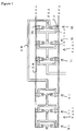
- Figure 1 shows a LSI pattern of two inverted amplifiers consisting of three MOS inverters serially connected.
- the first inverted amplifier INV1 consists of inverters I1, I2 and I3, and the second inverted amplifier INV2 consists of inverters I4, I5 and I6.
- inverters I1, I2, I3, I4, I5 and I6 there are shaped areas PL and NL made of p-layer and n-layer, respectively, an input and output lines PS1 and PS2 made of poly-silicon.
- the voltage Vdd and Vss of the power source and the ground are connected through metal lines M1 and M2 to the area PL and NL, respectively.
- I1, I2 and I3 are arranged from the right to the left, and I4, I5 and I6 are arranged from the left to the right.
- the first stage inverter I1 and I4 are shaped at the adjacent positions to each other. This positioning make the offset voltage of the inverters I1 and I4 substantially equal, because adjacent inverters are similar in characteristics according to experiences.
- an output of the inverter I3 is introduced through a metal line M3 to a position rightward from I1, and is connected to I4.
- dispersion of characteristic of the inverted amplifier is controlled to be minimum, and the accuracy is improved.
- the present invention can be applied not only to the above inverted amplifier but to any circuits including a plurality of MOS inverters serially connecting with the same characteristics.
- Figure 3 shows LSI pattern of inverted amplifier INV consisting of 3 stages MOS inverters, I1, I2 and I3.
- MOS inverters I1, I2 and I3.
- I1 and I2 there are shaped a common P-type semiconductor layer PL1 and a common N-type semiconductor layer NL1.
- P-type semiconductor layer PL2 and N-type semiconductor layer NL2 are shaped for I3.
- Drain voltage Vdd and source voltage Vss are connected to PL1 and NL1 through contacts C1 and C2.
- a contact is a metal part passing through in semiconductor layer in the direction of thickness, for electrical connection.
- the drain voltage Vdd and source voltage Vss are connected to PL2 and NL2 through contacts C7 and C8.
- the semiconductor layers PL1 and NL1 are provided with contacts C3 and C4 for an output from the first stage, respectively, and are provided with contacts C5 and C6 for an output from the second stage, respectively.
- the semiconductor layers PL2 and NL2 are provided with contacts C9 and C10 for an output from the third stage, respectively, from which an output is introduced through a poly-silicon portion PS toward the next stage.
- a strangulation portion S1 is provided between the contacts C1 and C5 in the semiconductor layer PL1, and a strangulation portion S3 is provided between the contacts C2 and C6 in the semiconductor layer NL1.
- a strangulation portion S2 is provided between contacts C7 and C9 in the semiconductor layers PL2, and a strangulation portion S4 is provided between contacts C8 and C10 in the semiconductor layer NL2.
- strangulation means S1 and S3 limit an electric current of the output of inverter I2, and it simultaneously decreases parasitic capacity of a transistor included in the inverter I2 by decreasing electric currency. A delay of performance of I2 due to the parasitic capacity is diminished, so the responsibility is highly improved.
- the strangulation portion causes an instability of output due to strangulated-channel-effect and increase of input side parasitic capacitance.
- these disadvantageous effect are not so influential in the second stage.
- the above advantageous effect is much more influential than the disadvantageous.
- the strangulation portions S2 and S4 limit an output electric currency of the inverter I3 of the final stage, and it is possible to save electrical power. Also in this stage, there is a possibility of disadvantageous effect above.
- the size of the strangulation portion should be decided so that the advantages are superior to the disadvantages.
- the present invention is not limited to the circuit of three stage MOS inverters, but can be adopted to a circuit including serially connected MOS inverters for which one common semiconductor layer with the same polarity is shaped.
- a MOS inverter circuit has a plurality of MOS inverters I 1 to I4 parallelly connected at their inputs and outputs, to which a single output voltage Vout is generated I response to a single input voltage Vin.
- Each MOS inverter is a CMOS inverter composed of pMOS type FET and nMOS type FET.
- a source of pMOS type FET is connected to a voltage Vdd of the power source.
- This parallel circuit has characteristics of an average characteristics of the total inverters, and dispersion of each element is compensated. Therefore, there is no problem of low accuracy due to dispersion of elements, so it is easy to produce LSI of high accuracy. This causes improvement of yield and cost performance of manufacturing.
- ⁇ p and ⁇ n are mobility of electron of pMOS type FET and nMOS type FET
- ⁇ and tox are dielectric constant and thickness of gate oxide layer per unit area
- Wp and Wn are channel width
- Lp and Ln are channel length. Dispersion of threshold value appears as a normal distribution in response to a value of ⁇ , however, formula 2 can not be analytically solved because it involves ⁇ of two terms. It is well known that a bi-polar transistor is improved in the quality by parallel connecting. Therefore, electrical elements parallelly connected have stable characteristics due to averaged characteristics of each element because the characteristics of the elements are statistically averaged.
- dispersion V1(Vin) of threshold voltage Vin shown by formula 1 is larger than a dispersion V2(Vin) of threshold voltage Vin shown by formula 2.
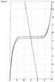
- Figure 5 is a graph showing voltage characteristic in a case that 2 inverters are parallelly connected.
- ⁇ - ⁇ shows a voltage Vin impressed to an input terminal
- ⁇ - ⁇ and ⁇ - ⁇ show characteristics of a single inverter
- ⁇ - ⁇ shows characteristics of two inverters parallelly connected.
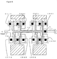
- Figure 6 shows a pattern in LSI of MOS inverter circuit.
- input and output of each MOS inverter are wired in a different layer, called input/output layer, from a layer, called semiconductor layer, where P-layer and N-layer of MOS are formed.
- the input and output are introduced through contact holes to the semiconductor layer.
- only one contact hole CH is commonly provided on the input side for four MOS inverters I1 to I4.
- input voltage is led to a gate of each MOS inverter from the contact hole CH through a poly-silicon PS.
- each of MOS inverters I1, I2, I3 and I4 there are provided two contact holes CH11 and CH12, CH21 and CH22, CH31 and CH32, CH41 and CH42, respectively.
- the outputs of pMOS and nMOS are led to the input/output layers from these contact holes.
- Outputs of each MOS inverter are connected to the circuit of the next stage through metallic wire M2.
- the contact hole is formed in square a side of which is longer than a width of the metallic wire.
- the embodiment above is advantageous because a lot of contact holes are neglected by a common contact hole for input. As a result, wiring is simplified and wiring area is decreased.
- Figure 7 shows an inverter circuit INV1 for obtaining inverted output V(OUT) with weight in response to an input voltage V(aIN1).
- the inverted circuit has one stage of MOS inverter I1, and its input is connected to V(aIN1) through input capacitance C1, and its output is connected to its input through a feedback capacitance Cf.
- V' of V(aIN1) is defined in formula 5 when power voltage is Vdd.
- V ' Vdd - ( C 1/ Cf ) V ( aIN 1)
- Figure 8 is a simulation result of V' and V(OUT) for their comparison by an analog circuit simulator Hspice.
- V(aIN1), V(OUT) and V' are shown by “ ⁇ ”, “ ⁇ ” and “ ⁇ ”, respectively.
- Vdd is equal to 3 [V]
- the following formula 6 is defined. 1 [V] ⁇ (aIN1) ⁇ 2 [V]
- V(aIN1) is equal to or more than 1 [V] and equal to or less than 2 [V]
- then V(OUT) is good approximation of V'.
- MOS inverter By an inversion with weight by MOS inverter of one stage, rather high accuracy can be obtained in an appropriate condition. Phase difference between input and output and consumed electricity is decreased because MOS inverter has only one stage.
- Figure 9 shows an inverter circuit INV1 for summation with weighting.
- This circuit includes input capacitances C1 and C2 parallelly connected to an input of a MOS inverter I1 of one stage.
- This embodiment is an embodiment similar to the fourth embodiment, but with the additional capacitance C2 parallel to the capacitance C1.
- An inverted summation is generated of weighted input voltages inputted to the first and the second capacitances.
- An output of the MOS inverter I1 is connected through a feedback capacitance Cf to its input.
- Input voltage (aIN1) and V(aIN2) are connected to input capacitances C1 and C2, and V(OUTp) is generated as an output voltage.
- a mathematically ideal value V' of inversion of weighted summation is defined in formula 7.
- V ' Vdd - ⁇ C 1 V ( aIN 1) + C 2 V ( a l N 2) ⁇ / Cf
- Figure 10 shows a practical output V(OUTp) simulated by Hspice, comparing with V'.
- V(aIN1), V(aIN2), V(OUTp) and V' are shown by " ⁇ ", " ⁇ ", " ⁇ ” and " ⁇ ”, respectively.
- V(OUT) is a good approximation of V(OUT) in the range of the following formulas 8 and 9.
- Formula 9 1 [V] ⁇ V [alN2] ⁇ 2 [V] As mentioned above, sufficiently high accuracy can be obtained by one stage MOS inverter.
- FIG 11 is a circuit of the sixth embodiment.
- An inverter circuit INV1 has MOS inverts I1 and I2 serially connected, each of which is one stage MOS inverter.
- Parallel input capacitances C1 and C2 are connected to an input of inverter I1.
- An output of the inverter I1 is connected to its input through a feedback a capacitance Cf1, and the output is connected to an input of the inverter I2 through connecting capacitance C4.
- An input capacitance C3 is further connected to the input of I2, parallelly to the capacitance C4.
- An output of inverter I2 is connected to the input through feedback capacitance Cf2.
- Input voltages V(1), V(2) and V(3) are connected to capacitances C1, C2 and C3.
- Inverter circuit INV1 consists of one stage MOS inverter I1, capacitances C1. C2 and Cf1, and inverter circuit INV2 consists of one stage MOS inverter I2, capacitances C4 and C3.
- the inverter circuit INV1 generates inverted output of summation of weighted voltages of V(1) and V(2), on the other hand, inverter circuit INV2 generates inverted output V(OUT) of weighted summation of an output from INV1 and the input V(3).
- V(OUT) A mathematical output of inverted summation with weighting is shown by formula 10, as V'.
- V(OUT) is a good approximation.
- FIG 12 is a circuit diagram showing the eighth embodiment.
- a plurality of input capacitances C1 to C4 are parallelly connected to a MOS inverter I1 of one stage. These capacitances are commonly connected to an input voltage V(1) through a multiplexers MUX1, MUX2, MUX3 and MUX4, respectively.
- the multiplexers connects the input voltage V(1) or the ground to the capacitances.
- An output of the inverter I1 is connected to its input through feedback capacitance Cf.
- V ' ( b 0 C 1+ b 1 C 2+ b 2 C 3+ b 3 C 4) V (1)/ Cf This is a normalized multiplication result of V(1) multiplied by a binary number consisting of bits b0 to b3. Simulation result is omitted, but V(OUT) is a good approximation of V'.
Landscapes
- Physics & Mathematics (AREA)
- Engineering & Computer Science (AREA)
- Computer Hardware Design (AREA)
- Computing Systems (AREA)
- General Engineering & Computer Science (AREA)
- Mathematical Physics (AREA)
- Metal-Oxide And Bipolar Metal-Oxide Semiconductor Integrated Circuits (AREA)
- Logic Circuits (AREA)
Priority Applications (1)
| Application Number | Priority Date | Filing Date | Title |
|---|---|---|---|
| EP00112801A EP1045446A3 (de) | 1994-09-30 | 1995-09-29 | MOS-Inverter mit einer verengten Kanalbreite |
Applications Claiming Priority (12)
| Application Number | Priority Date | Filing Date | Title |
|---|---|---|---|
| JP26162794 | 1994-09-30 | ||
| JP261627/94 | 1994-09-30 | ||
| JP6261627A JPH08102497A (ja) | 1994-09-30 | 1994-09-30 | Mosインバータ形成方法 |
| JP284496/94 | 1994-10-24 | ||
| JP6284496A JPH08125027A (ja) | 1994-10-24 | 1994-10-24 | Mosインバータ回路の形成方法 |
| JP28449694 | 1994-10-24 | ||
| JP30692594A JPH08148946A (ja) | 1994-11-16 | 1994-11-16 | インバータ回路 |
| JP30692594 | 1994-11-16 | ||
| JP306925/94 | 1994-11-16 | ||
| JP22461195 | 1995-08-09 | ||
| JP224611/95 | 1995-08-09 | ||
| JP22461195A JP3435417B2 (ja) | 1994-09-30 | 1995-08-09 | Mosインバータ |
Related Child Applications (1)
| Application Number | Title | Priority Date | Filing Date |
|---|---|---|---|
| EP00112801A Division EP1045446A3 (de) | 1994-09-30 | 1995-09-29 | MOS-Inverter mit einer verengten Kanalbreite |
Publications (3)
| Publication Number | Publication Date |
|---|---|
| EP0709892A2 true EP0709892A2 (de) | 1996-05-01 |
| EP0709892A3 EP0709892A3 (de) | 1998-11-04 |
| EP0709892B1 EP0709892B1 (de) | 2002-03-06 |
Family
ID=27477138
Family Applications (2)
| Application Number | Title | Priority Date | Filing Date |
|---|---|---|---|
| EP00112801A Withdrawn EP1045446A3 (de) | 1994-09-30 | 1995-09-29 | MOS-Inverter mit einer verengten Kanalbreite |
| EP95115447A Expired - Lifetime EP0709892B1 (de) | 1994-09-30 | 1995-09-29 | MOS-Inverter-Schaltung |
Family Applications Before (1)
| Application Number | Title | Priority Date | Filing Date |
|---|---|---|---|
| EP00112801A Withdrawn EP1045446A3 (de) | 1994-09-30 | 1995-09-29 | MOS-Inverter mit einer verengten Kanalbreite |
Country Status (3)
| Country | Link |
|---|---|
| US (2) | US5811859A (de) |
| EP (2) | EP1045446A3 (de) |
| DE (1) | DE69525707T2 (de) |
Families Citing this family (6)
| Publication number | Priority date | Publication date | Assignee | Title |
|---|---|---|---|---|
| JP3283210B2 (ja) * | 1997-05-30 | 2002-05-20 | 株式会社鷹山 | スペクトラム拡散通信方式における信号受信装置 |
| JPH11214528A (ja) * | 1998-01-29 | 1999-08-06 | Mitsubishi Electric Corp | 半導体装置 |
| JPH11338439A (ja) | 1998-03-27 | 1999-12-10 | Semiconductor Energy Lab Co Ltd | 半導体表示装置の駆動回路および半導体表示装置 |
| KR100687867B1 (ko) * | 2004-07-21 | 2007-02-27 | 주식회사 하이닉스반도체 | 저전력 고성능 인버터 회로 |
| US20150109025A1 (en) * | 2013-10-18 | 2015-04-23 | Qualcomm Incorporated | Area saving in latch arrays |
| CN111510137B (zh) * | 2020-06-04 | 2025-11-14 | 深圳比特微电子科技有限公司 | 时钟电路、计算芯片、算力板和数据处理设备 |
Family Cites Families (13)
| Publication number | Priority date | Publication date | Assignee | Title |
|---|---|---|---|---|
| JPS5740951A (en) * | 1980-08-25 | 1982-03-06 | Fujitsu Ltd | Manufacture of semiconductor device |
| EP0082208B1 (de) * | 1981-12-17 | 1985-11-21 | Deutsche ITT Industries GmbH | Integrierter CMOS-Schaltkreis |
| JPH0624319B2 (ja) * | 1983-03-18 | 1994-03-30 | 日本電気株式会社 | 入力回路 |
| JP2564787B2 (ja) * | 1983-12-23 | 1996-12-18 | 富士通株式会社 | ゲートアレー大規模集積回路装置及びその製造方法 |
| JPH06101551B2 (ja) * | 1985-11-30 | 1994-12-12 | 日本電信電話株式会社 | Cmos集積回路装置 |
| JPS63278248A (ja) * | 1987-03-13 | 1988-11-15 | Fujitsu Ltd | ゲ−トアレイの基本セル |
| JPH01202025A (ja) * | 1988-02-08 | 1989-08-15 | Mitsubishi Electric Corp | モード切替回路 |
| US5204990A (en) * | 1988-09-07 | 1993-04-20 | Texas Instruments Incorporated | Memory cell with capacitance for single event upset protection |
| JP2621612B2 (ja) * | 1990-08-11 | 1997-06-18 | 日本電気株式会社 | 半導体集積回路 |
| JPH0529548A (ja) * | 1991-07-23 | 1993-02-05 | Matsushita Electric Ind Co Ltd | 半導体装置及び半導体装置の製造方法 |
| US5306967A (en) * | 1992-05-29 | 1994-04-26 | Integrated Device Technology, Inc. | Apparatus for improving signal transmission along parallel lines |
| JP3055739B2 (ja) * | 1993-01-13 | 2000-06-26 | シャープ株式会社 | 乗算回路 |
| US5631863A (en) * | 1995-02-14 | 1997-05-20 | Honeywell Inc. | Random access memory cell resistant to radiation induced upsets |
-
1995
- 1995-09-29 DE DE69525707T patent/DE69525707T2/de not_active Expired - Fee Related
- 1995-09-29 EP EP00112801A patent/EP1045446A3/de not_active Withdrawn
- 1995-09-29 EP EP95115447A patent/EP0709892B1/de not_active Expired - Lifetime
-
1996
- 1996-11-04 US US08/743,161 patent/US5811859A/en not_active Expired - Fee Related
-
1997
- 1997-09-03 US US08/922,680 patent/US5917343A/en not_active Expired - Fee Related
Also Published As
| Publication number | Publication date |
|---|---|
| DE69525707D1 (de) | 2002-04-11 |
| EP1045446A3 (de) | 2000-11-15 |
| US5811859A (en) | 1998-09-22 |
| EP0709892B1 (de) | 2002-03-06 |
| US5917343A (en) | 1999-06-29 |
| DE69525707T2 (de) | 2002-08-01 |
| EP0709892A3 (de) | 1998-11-04 |
| EP1045446A2 (de) | 2000-10-18 |
Similar Documents
| Publication | Publication Date | Title |
|---|---|---|
| US7598541B2 (en) | Semiconductor device comprising transistor pair isolated by trench isolation | |
| US8338864B2 (en) | Semiconductor device | |
| KR890003147B1 (ko) | 게이트 에레이 | |
| US6172545B1 (en) | Delay circuit on a semiconductor device | |
| US7847638B2 (en) | Cascoded circuit | |
| US6849903B2 (en) | Basic cells configurable into different types of semiconductor integrated circuits | |
| US5442209A (en) | Synapse MOS transistor | |
| KR19980071343A (ko) | 발진회로 및 지연회로 | |
| US20060033525A1 (en) | Integrated header switch with low-leakage PMOS and high-leakage NMOS transistors | |
| EP0709892A2 (de) | Verfahren zur Ausgestaltung von MOS-Invertern | |
| EP0290857B1 (de) | Vorspannungseinrichtung, um eine spannungsunabhängige Kapazitanz zu verwirklichen | |
| KR100227583B1 (ko) | 반도체 장치 | |
| KR100331417B1 (ko) | 액정 표시 장치 | |
| US6744288B1 (en) | Driver with bulk switching MOS power transistor | |
| US5806054A (en) | Neuron MOSFET module structure for binary logic circuits | |
| JP3195203B2 (ja) | 半導体集積回路 | |
| EP0403267A2 (de) | Halbleiteranordnung | |
| US5602551A (en) | Analog-to-digital converter with silicon-on-insulator structure | |
| KR101270335B1 (ko) | 반도체 장치 | |
| EP0092176A2 (de) | Basiszelle für integrierte Verknüpfungsschaltungsfelder | |
| US6720214B2 (en) | Method for manufacturing semiconductor integrated circuit | |
| EP0337747B1 (de) | Schaltung für die Erzeugung einer Konstantspannung | |
| JP2840150B2 (ja) | 半導体集積回路及びその層間接続方法 | |
| JPH09148916A (ja) | 半導体集積回路 | |
| EP0373631B1 (de) | MOS-Transistor und Differentialverstärker mit niedrigem Offset |
Legal Events
| Date | Code | Title | Description |
|---|---|---|---|
| PUAI | Public reference made under article 153(3) epc to a published international application that has entered the european phase |
Free format text: ORIGINAL CODE: 0009012 |
|
| AK | Designated contracting states |
Kind code of ref document: A2 Designated state(s): DE FR GB |
|
| PUAL | Search report despatched |
Free format text: ORIGINAL CODE: 0009013 |
|
| AK | Designated contracting states |
Kind code of ref document: A3 Designated state(s): DE FR GB |
|
| 17P | Request for examination filed |
Effective date: 19990426 |
|
| 17Q | First examination report despatched |
Effective date: 19991103 |
|
| GRAG | Despatch of communication of intention to grant |
Free format text: ORIGINAL CODE: EPIDOS AGRA |
|
| RTI1 | Title (correction) |
Free format text: MOS INVERTER CIRCUIT |
|
| GRAG | Despatch of communication of intention to grant |
Free format text: ORIGINAL CODE: EPIDOS AGRA |
|
| GRAH | Despatch of communication of intention to grant a patent |
Free format text: ORIGINAL CODE: EPIDOS IGRA |
|
| GRAH | Despatch of communication of intention to grant a patent |
Free format text: ORIGINAL CODE: EPIDOS IGRA |
|
| REG | Reference to a national code |
Ref country code: GB Ref legal event code: IF02 |
|
| GRAA | (expected) grant |
Free format text: ORIGINAL CODE: 0009210 |
|
| AK | Designated contracting states |
Kind code of ref document: B1 Designated state(s): DE FR GB |
|
| REF | Corresponds to: |
Ref document number: 69525707 Country of ref document: DE Date of ref document: 20020411 |
|
| ET | Fr: translation filed | ||
| RAP2 | Party data changed (patent owner data changed or rights of a patent transferred) |
Owner name: SHARP KABUSHIKI KAISHA Owner name: YOZAN, INC. |
|
| PG25 | Lapsed in a contracting state [announced via postgrant information from national office to epo] |
Ref country code: GB Free format text: LAPSE BECAUSE OF NON-PAYMENT OF DUE FEES Effective date: 20020929 |
|
| PLBE | No opposition filed within time limit |
Free format text: ORIGINAL CODE: 0009261 |
|
| STAA | Information on the status of an ep patent application or granted ep patent |
Free format text: STATUS: NO OPPOSITION FILED WITHIN TIME LIMIT |
|
| 26N | No opposition filed |
Effective date: 20021209 |
|
| PG25 | Lapsed in a contracting state [announced via postgrant information from national office to epo] |
Ref country code: DE Free format text: LAPSE BECAUSE OF NON-PAYMENT OF DUE FEES Effective date: 20030401 |
|
| GBPC | Gb: european patent ceased through non-payment of renewal fee |
Effective date: 20020929 |
|
| PG25 | Lapsed in a contracting state [announced via postgrant information from national office to epo] |
Ref country code: FR Free format text: LAPSE BECAUSE OF NON-PAYMENT OF DUE FEES Effective date: 20030603 |
|
| REG | Reference to a national code |
Ref country code: FR Ref legal event code: ST |