EP0709896A1 - PNP-Lateraler Hochfrequenztransistor - Google Patents
PNP-Lateraler Hochfrequenztransistor Download PDFInfo
- Publication number
- EP0709896A1 EP0709896A1 EP94830500A EP94830500A EP0709896A1 EP 0709896 A1 EP0709896 A1 EP 0709896A1 EP 94830500 A EP94830500 A EP 94830500A EP 94830500 A EP94830500 A EP 94830500A EP 0709896 A1 EP0709896 A1 EP 0709896A1
- Authority
- EP
- European Patent Office
- Prior art keywords
- region
- base
- regions
- transistor
- emitter
- Prior art date
- Legal status (The legal status is an assumption and is not a legal conclusion. Google has not performed a legal analysis and makes no representation as to the accuracy of the status listed.)
- Granted
Links
- 239000004065 semiconductor Substances 0.000 claims 14
- 239000011810 insulating material Substances 0.000 claims 7
- 239000000463 material Substances 0.000 claims 7
- 239000002184 metal Substances 0.000 claims 6
- 125000006850 spacer group Chemical group 0.000 claims 5
- 230000015572 biosynthetic process Effects 0.000 claims 3
- 238000005755 formation reaction Methods 0.000 claims 3
- 239000004020 conductor Substances 0.000 claims 1
- 238000002955 isolation Methods 0.000 claims 1
- 239000000758 substrate Substances 0.000 claims 1
Images

Classifications
-
- H—ELECTRICITY
- H10—SEMICONDUCTOR DEVICES; ELECTRIC SOLID-STATE DEVICES NOT OTHERWISE PROVIDED FOR
- H10D—INORGANIC ELECTRIC SEMICONDUCTOR DEVICES
- H10D10/00—Bipolar junction transistors [BJT]
- H10D10/60—Lateral BJTs
Definitions
- the present invention relates to a high-frequency lateral PNP transistor.
- NPN transistors are the components most commonly used in both analog and digital bipolar integrated circuits, and, for them to also operate at high switching frequency, sophisticated fabrication techniques have been devised, such as: dielectric or trench isolation; using one or more polycrystalline silicon (polysilicon) layers; self-alignment by means of silicon oxide spacers or composite materials; rapid thermal processes (RTP); and using silicides and/or polycides (i.e. double layers formed of a layer of polysilicon and a layer of silicide).
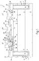
- NPN transistor structure developed by the present Applicant is shown in Figure 1 and described below.
- Figure 1 shows a cross section of a wafer of semiconductor material 1 including a P ⁇ type substrate 2; an N+ type buried layer 3; and an N ⁇ type epitaxial layer 4.
- a trench isolation region 5 peripherally defines the area (active area) in which the NPN transistor is formed, and comprises a nondoped polysilicon region 6 extending vertically from surface 35 of wafer 1, through epitaxial layer 4 and buried layer 3 to substrate 2; a nitride layer 7 surrounding polysilicon region 6 on all sides (except that facing surface 35 of wafer 1); and a thermal oxide layer 8 surrounding nitride layer 7.
- Field oxide regions 10, 11 extend across surface 35, the first over isolation region 5, and the second in an intermediate portion of the active area, so as to define two surface regions 12, 13 with no oxide covering.
- An N+ type sinker region 14 extends through epitaxial layer 4 from window 12 of surface 35 to buried layer 3; an N+ doped polysilicon layer 15 is formed over window 12, in electrical contact with sinker region 14; and a metal collector contact 16 is formed over layer 15.
- two P+ type regions 18, 19 are formed facing window 13 and connected to each other by a P type base region 20; two P+ doped polysilicon layers 22, 23 are formed over regions 18, 19, layer 23 of which also extends over field oxide region 11 presenting base contact 24; and oxide regions 25 cover regions 22, 23, 15 and field oxide regions 10, 11, with the exception of the areas in which collector and base contacts 16 and 24 are formed.
- regions 22, 23 and of overlying oxide regions 25 are covered with two symmetrical L-shaped thermal oxide portions 26, the horizontal arms of which cover part of surface 35 of wafer 1, and which are in turn covered by two L-shaped silicon nitride regions 27.
- Polysilicon layer 28, which forms an emitter region presents a thin N+ type layer 29 inside base region 20 and of a width equal to the distance between L-shaped regions 26; and a metal region 30 over polysilicon layer 28 forms the emitter contact of the transistor.
- the above structure provides for cutoff frequencies of over 20 GHz, propagation times of about 40 ps, and power-speed products of about 40 fJ.
- NPN transistors are the ones most commonly used in integrated circuits, situations exist in which PNP transistors are also desirable, e.g. for integrating complex logic or analog functions.
- Figure 2 shows one lateral PNP transistor structure proposed in an article by Yamaguchi et al. published in March 1994 in IEEE Transactions on Electron Devices, vol. 41, n. 3, p. 321-329.
- This known solution comprises a P ⁇ type substrate 40; an N+ type buried layer 41; an N type epitaxial layer 42; P+ type emitter and collector regions 43, 44 in epitaxial layer 42; and an N+ type sinker region 45 extending from the surface of the device to buried layer 41.
- a first oxide spacer region 48 separates emitter region 43 from collector region 44; and a second oxide spacer region 49 separates collector region 44 from sinker region 45; spacer regions 48, 49 are grown in the form of thermal oxide across the surface of the wafer.
- Polysilicon regions 50-52, doped similarly to regions 43-45, are deposited over the surface of the wafer at regions 43-45; and the emitter, collector and base contacts 53, 54, 55 are formed over regions 50-52.
- transistor current flows parallel to the surface; the P+ doped polysilicon regions 50 and 51 provide for contacting emitter region 43 and collector region 44; and the base region is formed by the portion 42' of epitaxial layer 42 extending between regions 43 and 44. Portion 42' is accessed by the low-resistivity path including polysilicon region 52, sinker region 45, and buried layer 41.
- the above known structure fails to provide for good static characteristics (in particular, it presents low h fe values), and dynamic performance is also unsatisfactory.
- the base width - indicated W B in Figure 2 and which determines the gain of the transistor - cannot be reduced to less than 2-2.5 ⁇ m on account of the alignment tolerances of the various layers, and the limits posed by the growth of spacer region 48 and by the presence of "bird beaks" growing beneath the oxidation mask, at the edges of the oxide region.
- the impossibility of accurately controlling the size of the "bird beaks" is also a major source of imprecision in the sizing of the base width.
- the thermal oxide layer is not grown across the surface over the base region between the emitter and collector, so that the base width does not depend on the thermal oxide growing process and is determined by other characteristics of the fabrication process, capable of achieving a reduction in minimum size and a greater accuracy.
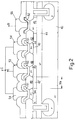
- Number 60 in Figure 3 indicates a silicon wafer comprising a P ⁇ type substrate 61, an N+ type buried layer 62 and an N ⁇ type epitaxial layer 63, similar to layers 2-4 in Figure 1.
- a trench isolation region 64 identical to region 5 in Figure 1 and therefore not described further, isolates the region in which the PNP transistor is formed from the adjacent regions in which other components are integrated.
- a field oxide region 66 extends across the surface 67 of the wafer, over isolation region 64, so as to peripherally define the active area of the PNP transistor.
- epitaxial layer 63 two spaced P+ type emitter and collector regions 68, 69 are formed facing surface 67; and, over emitter and collector regions 68, 69, there are formed two P+ doped polysilicon contact regions 70, 71 presenting a portion directly contacting surface 67 (and hence regions 68, 69), and a portion extending over field oxide region 66 where respective emitter and collector contacts 74 and 75 are formed.
- An oxide layer 76 covers regions 70, 71 and field oxide layers 66, with the exception of the areas in which emitter and collector contacts 74 and 75 are formed.
- regions 70, 71 and of overlying oxide layer 76 are covered with two symmetrical L-shaped portions of thermal oxide 77, the horizontal side of which covers part of surface 67 of wafer 1, and which are in turn covered with two symmetrical L-shaped silicon nitride regions 78.
- a substantially U-shaped polysilicon layer 80 doped to present N+ type conductivity, fills the gap between the horizontal arms of the L's contacting surface 67 of wafer 60, laterally covers nitride regions 78, and presents two horizontal end portions partially covering oxide layer 76.
- Polysilicon layer 80 which forms a base contact region, presents a thin N+ type layer 81 inside epitaxial layer 63; and a metal region 82 over polysilicon layer 80 forms the base contact of the transistor.
- the base region is formed by portion 63' of the epitaxial layer, the width (base width W B ) of which is defined by the distance between regions 68 and 69, and therefore substantially (with the exception of the lateral diffusion of regions 68, 69) by the distance between the facing edges of polysilicon regions 70 and 71.
- This distance is determined by a plasma etching photolithographic step, which technique provides for achieving smaller minimum dimensions and, though depending on the equipment used, far greater precision as compared with the thermal oxidation (planox) process used for growing oxide region 48 of the Figure 2 transistor. More specifically, the technique used by the Applicant provides for achieving a base width W B of about 0.8 ⁇ m.
- the polysilicon layer 80 between regions 70 and 71 provides for minimizing the extrinsic base resistance r bb , of the transistor, as well as for dispensing with the sinker region normally provided between the base contact and the epitaxial layer (region 14 in Figure 1 and 45 in Figure 2), thus greatly reducing the size of the transistor and hence the parasitic capacitances associated with it.
- the Figure 3 transistor also provides for improving gain by permitting the use of a less heavily doped epitaxial layer 63 as compared with the known Figure 2 solution.
- the Figure 3 transistor presents superior dynamic and static characteristics ensuring reliable operation even at high frequency.
- the Figure 3 transistor presents the same structure as in Figure 1, and may therefore be formed using the same technology and simultaneously with the Figure 1 transistor. More specifically, regions 70 and 71 may be formed simultaneously with regions 22, 23 in Figure 1, and, like regions 22, 23 for regions 18, 19, constitute diffusion sources for emitter and collector regions 68 and 69, which are thus formed by dope diffusion from regions 70 and 71, with no need for specific implant or diffusion steps. Similarly, spacer regions 77, 78 and N+ doped polysilicon region 80 may be formed simultaneously with corresponding spacer regions 26, 27 and polysilicon region 28 in Figure 1, by appropriately modifying the mask. A special mask must be provided, however, to prevent the base implant for forming region 20 in Figure 1 from penetrating the base region of the Figure 3 transistor.
- the minimum base width is determined by the need to prevent the two horizontal arms of the L's from touching during the successive steps for defining spacer regions 77 and 78; which condition therefore imposes a minimum distance between polysilicon emitter and collector regions 70, 71, and hence a minimum base width W B .
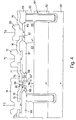
- the distance between polysilicon emitter and collector regions 70 and 71 is so selected that the two horizontal arms of the two L-shaped spacer regions 77 in Figure 3 are no more separated, and are joined to form a single U-shaped oxide spacer region 85.
- nitride regions 78 are joined to form a single U-shaped nitride region 86; and a field oxide region 87 is formed across the surface of the wafer to divide the active area into two parts: one integrating emitter and collector regions 68, 69 and the base region (portion 63'' of the epitaxial layer), and a part in which is formed an N+ type sinker region 88 extending from surface 67 to buried layer 62.
- an N+ doped polysilicon layer 89 is formed with a base contact 90 on top.
- the N+ doped silicon layer for forming region 89 of the Figure 4 transistor is easily removable from surface 67 at base region 63''.
- region 80 cannot be removed, due to the risk of over-etching down to the epitaxial layer and so damaging the base region; whereas, in the second embodiment in Figure 4, the N+ polysilicon layer may safely be removed by virtue of epitaxial layer 63 at base region 63'' being protected by oxide and nitride regions 85, 86.
- metal line 74 forming the emitter contact is extended over base region 63'' to prevent the formation of inverted surface layers between the emitter and collector.
- Figure 4 embodiment involves no changes to the fabrication process of the Figure 1 NPN transistor.
- the advantages of the transistor according to the present invention are as follows.
- eliminating the field oxide layer across the surface over the base region greatly reduces the base width and hence increases the gain of the transistor; and reducing the size and defectiveness of the transistor provides for improved dynamic performance, as well as for permitting use of the transistor in high-frequency applications.
Landscapes
- Bipolar Transistors (AREA)
Priority Applications (3)
| Application Number | Priority Date | Filing Date | Title |
|---|---|---|---|
| EP94830500A EP0709896B1 (de) | 1994-10-26 | 1994-10-26 | Verfahren zur Herstellung eines lateralen PNP-Hochfrequenztransistors |
| DE69433965T DE69433965D1 (de) | 1994-10-26 | 1994-10-26 | Verfahren zur Herstellung eines lateralen PNP-Hochfrequenztransistors |
| US08/547,881 US5796157A (en) | 1994-10-26 | 1995-10-25 | High-frequency lateral PNP transistor |
Applications Claiming Priority (1)
| Application Number | Priority Date | Filing Date | Title |
|---|---|---|---|
| EP94830500A EP0709896B1 (de) | 1994-10-26 | 1994-10-26 | Verfahren zur Herstellung eines lateralen PNP-Hochfrequenztransistors |
Publications (2)
| Publication Number | Publication Date |
|---|---|
| EP0709896A1 true EP0709896A1 (de) | 1996-05-01 |
| EP0709896B1 EP0709896B1 (de) | 2004-08-25 |
Family
ID=8218555
Family Applications (1)
| Application Number | Title | Priority Date | Filing Date |
|---|---|---|---|
| EP94830500A Expired - Lifetime EP0709896B1 (de) | 1994-10-26 | 1994-10-26 | Verfahren zur Herstellung eines lateralen PNP-Hochfrequenztransistors |
Country Status (3)
| Country | Link |
|---|---|
| US (1) | US5796157A (de) |
| EP (1) | EP0709896B1 (de) |
| DE (1) | DE69433965D1 (de) |
Cited By (1)
| Publication number | Priority date | Publication date | Assignee | Title |
|---|---|---|---|---|
| EP0881688A1 (de) * | 1997-05-30 | 1998-12-02 | STMicroelectronics S.r.l. | Elektronisches Bauelement vom Typ lateral-bipolar-pnp |
Families Citing this family (6)
| Publication number | Priority date | Publication date | Assignee | Title |
|---|---|---|---|---|
| DE69714575D1 (de) * | 1997-05-30 | 2002-09-12 | St Microelectronics Srl | Laterales PNP-bipolares elektronisches Bauelement und dessen Herstellungsverfahren |
| US6774001B2 (en) * | 1998-10-13 | 2004-08-10 | Stmicroelectronics, Inc. | Self-aligned gate and method |
| US6900105B2 (en) * | 2000-03-01 | 2005-05-31 | Freescale Semiconductor, Inc. | Semiconductor device and method of manufacture |
| JP2007180242A (ja) * | 2005-12-27 | 2007-07-12 | Sanyo Electric Co Ltd | 半導体装置及びその製造方法 |
| US8878344B2 (en) | 2012-10-18 | 2014-11-04 | Analog Devices, Inc. | Compound semiconductor lateral PNP bipolar transistors |
| US9502504B2 (en) * | 2013-12-19 | 2016-11-22 | International Business Machines Corporation | SOI lateral bipolar transistors having surrounding extrinsic base portions |
Citations (2)
| Publication number | Priority date | Publication date | Assignee | Title |
|---|---|---|---|---|
| JPS6358870A (ja) * | 1986-08-29 | 1988-03-14 | Fujitsu Ltd | 半導体装置の製造方法 |
| EP0526374A1 (de) * | 1991-07-19 | 1993-02-03 | International Business Machines Corporation | Lateraler Bipolar-Transistor und Verfahren zu seiner Herstellung |
Family Cites Families (2)
| Publication number | Priority date | Publication date | Assignee | Title |
|---|---|---|---|---|
| KR100234550B1 (ko) * | 1990-04-02 | 1999-12-15 | 클라크 3세 존 엠 | 증가된 항복 전압을 지닌 트랜지스터 디바이스 및 제조방법 |
| JPH0793316B2 (ja) * | 1992-12-28 | 1995-10-09 | 日本電気株式会社 | 半導体装置の製造方法 |
-
1994
- 1994-10-26 EP EP94830500A patent/EP0709896B1/de not_active Expired - Lifetime
- 1994-10-26 DE DE69433965T patent/DE69433965D1/de not_active Expired - Lifetime
-
1995
- 1995-10-25 US US08/547,881 patent/US5796157A/en not_active Expired - Lifetime
Patent Citations (2)
| Publication number | Priority date | Publication date | Assignee | Title |
|---|---|---|---|---|
| JPS6358870A (ja) * | 1986-08-29 | 1988-03-14 | Fujitsu Ltd | 半導体装置の製造方法 |
| EP0526374A1 (de) * | 1991-07-19 | 1993-02-03 | International Business Machines Corporation | Lateraler Bipolar-Transistor und Verfahren zu seiner Herstellung |
Non-Patent Citations (5)
| Title |
|---|
| E. BERNDLMAIER ET AL.: "Lateral PNP transistor with minimal basewidth", IBM TECHNICAL DISCLOSURE BULLETIN, vol. 22, no. 10, March 1980 (1980-03-01), NEW YORK US, pages 4543 * |
| P.C. HUNT: "Bipolar device design for high density high performance applications", INTERNATIONAL ELECTRON DEVICES MEETING TECHNICAL DIGEST 1989, December 1989 (1989-12-01), WASHINGTON, DC, USA, pages 791 - 794, XP000448310 * |
| PATENT ABSTRACTS OF JAPAN vol. 12, no. 281 (E - 641)<3128> 2 August 1988 (1988-08-02) * |
| T. YAMAGUCHI ET AL.: "Process investigations for a 30-GHz ft submicrometer double poly-si bipolar technology", IEEE TRANSACTIONS ON ELECTRON DEVICES, vol. 41, no. 3, March 1994 (1994-03-01), NEW YORK US, pages 321 - 329 * |
| T.H. NING: "Narrow-base epitaxial-base lateral PNP", IBM TECHNICAL DISCLOSURE BULLETIN, vol. 25, no. 8, January 1983 (1983-01-01), NEW YORK US, pages 4171 - 4173 * |
Cited By (2)
| Publication number | Priority date | Publication date | Assignee | Title |
|---|---|---|---|---|
| EP0881688A1 (de) * | 1997-05-30 | 1998-12-02 | STMicroelectronics S.r.l. | Elektronisches Bauelement vom Typ lateral-bipolar-pnp |
| US6198154B1 (en) | 1997-05-30 | 2001-03-06 | Stmicroelectronics, S.R.L. | PNP lateral bipolar electronic device |
Also Published As
| Publication number | Publication date |
|---|---|
| DE69433965D1 (de) | 2004-09-30 |
| EP0709896B1 (de) | 2004-08-25 |
| US5796157A (en) | 1998-08-18 |
Similar Documents
| Publication | Publication Date | Title |
|---|---|---|
| US5428243A (en) | Bipolar transistor with a self-aligned heavily doped collector region and base link regions. | |
| US5516710A (en) | Method of forming a transistor | |
| US7462547B2 (en) | Method of fabricating a bipolar transistor having reduced collector-base capacitance | |
| US4908324A (en) | Method of manufacturing bipolar transistor | |
| JPH0420265B2 (de) | ||
| US20210134987A1 (en) | Gate controlled lateral bipolar junction/heterojunction transistors | |
| US7968416B2 (en) | Integrated circuit arrangement with NPN and PNP bipolar transistors and corresponding production method | |
| US4738624A (en) | Bipolar transistor structure with self-aligned device and isolation and fabrication process therefor | |
| US20030193077A1 (en) | Bipolar transistor and method of fabricating the same | |
| US5098853A (en) | Self-aligned, planar heterojunction bipolar transistor and method of forming the same | |
| KR100474867B1 (ko) | 반도체장치 및 그 제조방법 | |
| US5796157A (en) | High-frequency lateral PNP transistor | |
| US20030107051A1 (en) | Super self -aligned heterojunction biplar transistor and its manufacturing method | |
| US5198375A (en) | Method for forming a bipolar transistor structure | |
| EP1842229B1 (de) | Bipolartransistor und herstellungsverfahren dafür | |
| US20250120144A1 (en) | Bipolar transistor structures with cavity below extrinsic base and methods to form same | |
| KR20020032425A (ko) | 콜렉터-업 rf 전력 트랜지스터 | |
| US5159423A (en) | Self-aligned, planar heterojunction bipolar transistor | |
| EP0036499A1 (de) | Ein selbstjustierendes Verfahren für einen Bipolartransistor auf Polysilicium-Basis | |
| US20050037587A1 (en) | Heterojunction bipolar transistor | |
| US5070028A (en) | Method for manufacturing bipolar transistors having extremely reduced base-collection capacitance | |
| US7723198B2 (en) | Integrated semiconductor cascode circuit for high-frequency applications | |
| EP1184910B1 (de) | Widerstand mit Feldplatte und mit darüber angeordnetem und erweiterten Leitweglenkungsgebiet | |
| US6146956A (en) | PNP lateral bipolar electronic device and corresponding manufacturing process | |
| KR100761561B1 (ko) | 반도체 디바이스 제조 방법 |
Legal Events
| Date | Code | Title | Description |
|---|---|---|---|
| PUAI | Public reference made under article 153(3) epc to a published international application that has entered the european phase |
Free format text: ORIGINAL CODE: 0009012 |
|
| 17P | Request for examination filed |
Effective date: 19951130 |
|
| AK | Designated contracting states |
Kind code of ref document: A1 Designated state(s): DE FR GB IT |
|
| 17Q | First examination report despatched |
Effective date: 19961120 |
|
| GRAP | Despatch of communication of intention to grant a patent |
Free format text: ORIGINAL CODE: EPIDOSNIGR1 |
|
| RIC1 | Information provided on ipc code assigned before grant |
Ipc: 7H 01L 29/735 B Ipc: 7H 01L 21/331 A |
|
| RTI1 | Title (correction) |
Free format text: METHOD FOR MANUFACTURING A HIGH-FREQUENCY LATERAL PNP TRANSISTOR |
|
| GRAS | Grant fee paid |
Free format text: ORIGINAL CODE: EPIDOSNIGR3 |
|
| GRAA | (expected) grant |
Free format text: ORIGINAL CODE: 0009210 |
|
| AK | Designated contracting states |
Kind code of ref document: B1 Designated state(s): DE FR GB IT |
|
| PG25 | Lapsed in a contracting state [announced via postgrant information from national office to epo] |
Ref country code: FR Free format text: LAPSE BECAUSE OF FAILURE TO SUBMIT A TRANSLATION OF THE DESCRIPTION OR TO PAY THE FEE WITHIN THE PRESCRIBED TIME-LIMIT Effective date: 20040825 |
|
| REG | Reference to a national code |
Ref country code: GB Ref legal event code: FG4D |
|
| REF | Corresponds to: |
Ref document number: 69433965 Country of ref document: DE Date of ref document: 20040930 Kind code of ref document: P |
|
| PG25 | Lapsed in a contracting state [announced via postgrant information from national office to epo] |
Ref country code: DE Free format text: LAPSE BECAUSE OF FAILURE TO SUBMIT A TRANSLATION OF THE DESCRIPTION OR TO PAY THE FEE WITHIN THE PRESCRIBED TIME-LIMIT Effective date: 20041126 |
|
| PLBE | No opposition filed within time limit |
Free format text: ORIGINAL CODE: 0009261 |
|
| STAA | Information on the status of an ep patent application or granted ep patent |
Free format text: STATUS: NO OPPOSITION FILED WITHIN TIME LIMIT |
|
| 26N | No opposition filed |
Effective date: 20050526 |
|
| EN | Fr: translation not filed | ||
| PG25 | Lapsed in a contracting state [announced via postgrant information from national office to epo] |
Ref country code: IT Free format text: LAPSE BECAUSE OF NON-PAYMENT OF DUE FEES;WARNING: LAPSES OF ITALIAN PATENTS WITH EFFECTIVE DATE BEFORE 2007 MAY HAVE OCCURRED AT ANY TIME BEFORE 2007. THE CORRECT EFFECTIVE DATE MAY BE DIFFERENT FROM THE ONE RECORDED. Effective date: 20051026 |
|
| PGFP | Annual fee paid to national office [announced via postgrant information from national office to epo] |
Ref country code: GB Payment date: 20060327 Year of fee payment: 12 |
|
| GBPC | Gb: european patent ceased through non-payment of renewal fee |
Effective date: 20061026 |
|
| PG25 | Lapsed in a contracting state [announced via postgrant information from national office to epo] |
Ref country code: GB Free format text: LAPSE BECAUSE OF NON-PAYMENT OF DUE FEES Effective date: 20061026 |