EP0881688A1 - Elektronisches Bauelement vom Typ lateral-bipolar-pnp - Google Patents
Elektronisches Bauelement vom Typ lateral-bipolar-pnp Download PDFInfo
- Publication number
- EP0881688A1 EP0881688A1 EP97830257A EP97830257A EP0881688A1 EP 0881688 A1 EP0881688 A1 EP 0881688A1 EP 97830257 A EP97830257 A EP 97830257A EP 97830257 A EP97830257 A EP 97830257A EP 0881688 A1 EP0881688 A1 EP 0881688A1
- Authority
- EP
- European Patent Office
- Prior art keywords
- lateral pnp
- doped
- region
- active area
- electronic device
- Prior art date
- Legal status (The legal status is an assumption and is not a legal conclusion. Google has not performed a legal analysis and makes no representation as to the accuracy of the status listed.)
- Ceased
Links
- 239000000758 substrate Substances 0.000 claims abstract description 23
- 239000004065 semiconductor Substances 0.000 claims abstract description 18
- 239000012535 impurity Substances 0.000 claims description 4
- 230000003321 amplification Effects 0.000 abstract description 3
- 238000003199 nucleic acid amplification method Methods 0.000 abstract description 3
- 230000003071 parasitic effect Effects 0.000 description 6
- 230000008901 benefit Effects 0.000 description 5
- 230000000694 effects Effects 0.000 description 4
- 241000293849 Cordylanthus Species 0.000 description 3
- 238000009792 diffusion process Methods 0.000 description 3
- 239000002019 doping agent Substances 0.000 description 3
- 238000000034 method Methods 0.000 description 3
- 230000015572 biosynthetic process Effects 0.000 description 2
- 239000000969 carrier Substances 0.000 description 2
- 238000010586 diagram Methods 0.000 description 2
- 238000000635 electron micrograph Methods 0.000 description 2
- 238000012876 topography Methods 0.000 description 2
- 230000002411 adverse Effects 0.000 description 1
- 230000015556 catabolic process Effects 0.000 description 1
- 230000008021 deposition Effects 0.000 description 1
- 238000002955 isolation Methods 0.000 description 1
- 238000004519 manufacturing process Methods 0.000 description 1
- 230000000873 masking effect Effects 0.000 description 1
- 230000002093 peripheral effect Effects 0.000 description 1
- 229910021420 polycrystalline silicon Inorganic materials 0.000 description 1
- 229920005591 polysilicon Polymers 0.000 description 1
Images


Classifications
-
- H—ELECTRICITY
- H10—SEMICONDUCTOR DEVICES; ELECTRIC SOLID-STATE DEVICES NOT OTHERWISE PROVIDED FOR
- H10D—INORGANIC ELECTRIC SEMICONDUCTOR DEVICES
- H10D64/00—Electrodes of devices having potential barriers
- H10D64/20—Electrodes characterised by their shapes, relative sizes or dispositions
- H10D64/23—Electrodes carrying the current to be rectified, amplified, oscillated or switched, e.g. sources, drains, anodes or cathodes
- H10D64/231—Emitter or collector electrodes for bipolar transistors
-
- H—ELECTRICITY
- H10—SEMICONDUCTOR DEVICES; ELECTRIC SOLID-STATE DEVICES NOT OTHERWISE PROVIDED FOR
- H10D—INORGANIC ELECTRIC SEMICONDUCTOR DEVICES
- H10D10/00—Bipolar junction transistors [BJT]
- H10D10/60—Lateral BJTs
-
- H—ELECTRICITY
- H10—SEMICONDUCTOR DEVICES; ELECTRIC SOLID-STATE DEVICES NOT OTHERWISE PROVIDED FOR
- H10D—INORGANIC ELECTRIC SEMICONDUCTOR DEVICES
- H10D84/00—Integrated devices formed in or on semiconductor substrates that comprise only semiconducting layers, e.g. on Si wafers or on GaAs-on-Si wafers
- H10D84/60—Integrated devices formed in or on semiconductor substrates that comprise only semiconducting layers, e.g. on Si wafers or on GaAs-on-Si wafers characterised by the integration of at least one component covered by groups H10D10/00 or H10D18/00, e.g. integration of BJTs
- H10D84/641—Combinations of only vertical BJTs
Definitions
- This invention relates to a PNP bipolar electronic device.
- the invention relates to a lateral PNP bipolar electronic device which is integrated monolithically on a semiconductor substrate together with other bipolar devices of the NPN type; said device being incorporated into an electrically insulated multilayer structure which comprises:
- NPN transistors are preferred for implementing integrated circuitry of the bipolar type on semiconductor substrates, on account of their CC and AC amplifications being definitely better than those of PNP transistors.
- PNP bipolar transistors Another disadvantage of PNP bipolar transistors is their close limitations in high frequency applications.
- PNP transistors on a semiconductor substrate is effected concurrently with that of NPN transistors, without any additional implanting or masking steps.
- PNP bipolar transistors of the so-called lateral type such that they can be compatible with the process flows adopted to fabricate NPN bipolar devices.
- Figure 1 shows an enlarged cross-sectional view, taken on a vertical plane, of a sidewall PNP device 6 formed on a P-doped semiconductor substrate 1.
- a first buried layer 2 doped N+ to form the base region of the transistor and a second layer 3, doped N, which constitutes the active area of the PNP device to be.
- lateral PNP transistors have an intrinsic current loss of about 3% compared to collector current; these currents can also be explained theoretically by having reference to the diagram in Figure 2 of an equivalent electric circuit of a lateral PNP transistor.
- the lateral PNP device designated Q 1 in the equivalent circuit, is connected to a pair of parasitic PNP transistors Q 2 and Q 3 having their respective emitter regions connected to the emitter and collector regions of the transistor Q 1 .
- parasitic devices Q 2 and Q 3 have their collector regions connected to the semiconductor substrate, and their base regions in common with the base of Q 1 .
- This equivalent electric diagram shows that the parasitic currents are mainly attributable to the second parasitic device Q 2 draining toward the substrate some of the current being injected by the emitter of Q 1 , thereby lowering the efficiency of lateral emission.
- lateral PNP transistors have been implemented conventionally with their emitter region occupying, in the active area, a central location surrounded by two collector regions.
- this prior solution has a serious drawback in that it leads to increased values of certain characteristic parameters of the lateral PNP device, such as the base-collector and emitter-base capacitances, C bc and C eb , which restrict performance at high frequencies.
- the B* factor is inversely proportional to the passage time through the base region, so that as it increases, the frequency performance of the lateral PNP device deteriorates.
- the width W b of the base region of the lateral PNP transistors always exhibits values between 2 ⁇ m and 4 ⁇ m.
- the central emitter region includes neighbouring regions with a predetermined width E c , due to the "bird's beak" phenomenon.
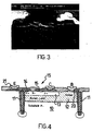
- Figure 3 shows an enlarged cross-section through a typical lateral PNP device taken near the central emitter region.
- the "bird's beak" inside the active area extends for about 0.6 ⁇ m and, therefore, retires a minimum width W AA greater than 2.6 ⁇ m.
- the technical problem underlying this invention is to provide a new topography conferring, on a lateral PNP device, such structural and functional features as to make it suitable for high frequency applications as well, thereby overcoming the aforesaid limitations and drawbacks.
- the solution idea behind this invention is to provide a lateral PNP device topography which is compatible with NPN process flows and allows an emitter region to be located peripherally of the active area of the device rather than centrally.
- the design of the lateral PNP device of this invention provides a better figure of merit than conventional lateral PNP transistors.
- a lateral PNP device 15 monolithically integrated on a semiconductor substrate together with other NPN devices (not shown because conventional) which can also be operated at high frequencies, will be described.
- This multilayer structure is produced by the successive deposition, onto the substrate 10, of a first buried layer 12 doped for conductivity of the N type to form a base region, and of a second layer 13 with conductivity of the N type which represents an active area of the lateral PNP device 15.
- the fabrication process includes the definition of an emitter region 14 and a collector region 15.
- a first step of selectively diffusing P-type dopants is carried out onto the surface of the active area.
- the emitter region 14 will locate peripherally of the active area, opposite from the collector region 15.
- a second step of diffusing N dopants is carried out so as to have the base region of the first buried layer extended to the top of the multilayer structure.
- This step is carried out conventionally to provide polysilicon electric contacts at the locations of the emitter 14, collector 15 and base 20 regions.
- the contacts are formed in predetermined areas of the multilayer structure top, taking care to provide an emitter contact 21 externally of the multilayer structure of the PNP device 15.
- the layout described so far has the advantage of reducing the capacitive parameters, C be and C bc , associated with the lateral PNP device 15 which were the main cause of limitation to performance at high frequencies.
- the solution proposed herein may seem a tradeoff of the collection efficiency brought about by a single collector region 15 (hence, an inferior collector current) in favor of improved performance at high frequencies.
- the emitter region 14 is preferably rectangular in plan form, with a width W e smaller than its length L e . This region 14 locates oppposite from the central collector region 15 (omitted from Figures 5 and 6).
- this geometry of the emitter region 14 has added advantages to further reduce the value of the capacitive parameter C eb and to reduce current leakage toward the substrate 10.
- 'active periphery P' is used herein to indicate that portion of the emitter region 14 perimeter which is facing the collector region 15 directly.
- this P/A ratio can reach very high values, previously unattainable by a standard PNP device having a central emitter region.
- the P/A ration is equal to a constant, 1/W e , obtained from respective values of P and A equal to L e and W e *L e .
- this lateral PNP device can be operated at high frequencies, with suitable collector current values and good amplification, to provide a superior figure of merit compared to that typical of conventional lateral PNP devices.
Landscapes
- Bipolar Transistors (AREA)
- Bipolar Integrated Circuits (AREA)
Priority Applications (3)
| Application Number | Priority Date | Filing Date | Title |
|---|---|---|---|
| EP97830257A EP0881688A1 (de) | 1997-05-30 | 1997-05-30 | Elektronisches Bauelement vom Typ lateral-bipolar-pnp |
| US09/087,421 US6198154B1 (en) | 1997-05-30 | 1998-05-29 | PNP lateral bipolar electronic device |
| US09/735,231 US20010000413A1 (en) | 1997-05-30 | 2000-12-11 | PNP lateral bipolar electronic device |
Applications Claiming Priority (1)
| Application Number | Priority Date | Filing Date | Title |
|---|---|---|---|
| EP97830257A EP0881688A1 (de) | 1997-05-30 | 1997-05-30 | Elektronisches Bauelement vom Typ lateral-bipolar-pnp |
Publications (1)
| Publication Number | Publication Date |
|---|---|
| EP0881688A1 true EP0881688A1 (de) | 1998-12-02 |
Family
ID=8230650
Family Applications (1)
| Application Number | Title | Priority Date | Filing Date |
|---|---|---|---|
| EP97830257A Ceased EP0881688A1 (de) | 1997-05-30 | 1997-05-30 | Elektronisches Bauelement vom Typ lateral-bipolar-pnp |
Country Status (2)
| Country | Link |
|---|---|
| US (2) | US6198154B1 (de) |
| EP (1) | EP0881688A1 (de) |
Cited By (1)
| Publication number | Priority date | Publication date | Assignee | Title |
|---|---|---|---|---|
| CN107895739A (zh) * | 2017-12-07 | 2018-04-10 | 湖南大学 | 一种适合单片集成的高速高增益横向bjt结构及制备方法 |
Families Citing this family (4)
| Publication number | Priority date | Publication date | Assignee | Title |
|---|---|---|---|---|
| DE69714575D1 (de) * | 1997-05-30 | 2002-09-12 | St Microelectronics Srl | Laterales PNP-bipolares elektronisches Bauelement und dessen Herstellungsverfahren |
| US6551869B1 (en) * | 2000-06-09 | 2003-04-22 | Motorola, Inc. | Lateral PNP and method of manufacture |
| US7585740B2 (en) * | 2006-03-14 | 2009-09-08 | International Business Machines Corporation | Fully silicided extrinsic base transistor |
| US10553633B2 (en) * | 2014-05-30 | 2020-02-04 | Klaus Y.J. Hsu | Phototransistor with body-strapped base |
Citations (5)
| Publication number | Priority date | Publication date | Assignee | Title |
|---|---|---|---|---|
| EP0039411A2 (de) * | 1980-05-05 | 1981-11-11 | International Business Machines Corporation | Herstellungsverfahren einer integrierten PNP- und NPN-Transistorstruktur |
| JPH0240922A (ja) * | 1988-07-31 | 1990-02-09 | Nec Corp | 半導体装置 |
| EP0435308A1 (de) * | 1989-12-28 | 1991-07-03 | Kabushiki Kaisha Toshiba | Laterales Halbleiterbauelement |
| US5397912A (en) * | 1991-12-02 | 1995-03-14 | Motorola, Inc. | Lateral bipolar transistor |
| EP0709896A1 (de) * | 1994-10-26 | 1996-05-01 | Consorzio per la Ricerca sulla Microelettronica nel Mezzogiorno - CoRiMMe | PNP-Lateraler Hochfrequenztransistor |
Family Cites Families (4)
| Publication number | Priority date | Publication date | Assignee | Title |
|---|---|---|---|---|
| US4115797A (en) * | 1976-10-04 | 1978-09-19 | Fairchild Camera And Instrument Corporation | Integrated injection logic with heavily doped injector base self-aligned with injector emitter and collector |
| DE2757762C2 (de) * | 1977-12-23 | 1985-03-07 | Siemens AG, 1000 Berlin und 8000 München | Monolithische Kombination zweier komplementärer Bipolartransistoren |
| EP0642170B1 (de) * | 1990-02-22 | 1997-12-03 | Canon Kabushiki Kaisha | Lateraler Bipolartransistor |
| JP2859760B2 (ja) * | 1991-07-26 | 1999-02-24 | ローム株式会社 | ラテラルトランジスタおよびその製法 |
-
1997
- 1997-05-30 EP EP97830257A patent/EP0881688A1/de not_active Ceased
-
1998
- 1998-05-29 US US09/087,421 patent/US6198154B1/en not_active Expired - Lifetime
-
2000
- 2000-12-11 US US09/735,231 patent/US20010000413A1/en not_active Abandoned
Patent Citations (5)
| Publication number | Priority date | Publication date | Assignee | Title |
|---|---|---|---|---|
| EP0039411A2 (de) * | 1980-05-05 | 1981-11-11 | International Business Machines Corporation | Herstellungsverfahren einer integrierten PNP- und NPN-Transistorstruktur |
| JPH0240922A (ja) * | 1988-07-31 | 1990-02-09 | Nec Corp | 半導体装置 |
| EP0435308A1 (de) * | 1989-12-28 | 1991-07-03 | Kabushiki Kaisha Toshiba | Laterales Halbleiterbauelement |
| US5397912A (en) * | 1991-12-02 | 1995-03-14 | Motorola, Inc. | Lateral bipolar transistor |
| EP0709896A1 (de) * | 1994-10-26 | 1996-05-01 | Consorzio per la Ricerca sulla Microelettronica nel Mezzogiorno - CoRiMMe | PNP-Lateraler Hochfrequenztransistor |
Non-Patent Citations (1)
| Title |
|---|
| PATENT ABSTRACTS OF JAPAN vol. 014, no. 194 (E - 0919) 20 April 1990 (1990-04-20) * |
Cited By (1)
| Publication number | Priority date | Publication date | Assignee | Title |
|---|---|---|---|---|
| CN107895739A (zh) * | 2017-12-07 | 2018-04-10 | 湖南大学 | 一种适合单片集成的高速高增益横向bjt结构及制备方法 |
Also Published As
| Publication number | Publication date |
|---|---|
| US20010000413A1 (en) | 2001-04-26 |
| US6198154B1 (en) | 2001-03-06 |
Similar Documents
| Publication | Publication Date | Title |
|---|---|---|
| US4546536A (en) | Fabrication methods for high performance lateral bipolar transistors | |
| US6737722B2 (en) | Lateral transistor having graded base region, semiconductor integrated circuit and fabrication method thereof | |
| US4038680A (en) | Semiconductor integrated circuit device | |
| CA1145062A (en) | Semiconductor device | |
| US6198154B1 (en) | PNP lateral bipolar electronic device | |
| JP2628988B2 (ja) | 半導体装置及びその製造方法 | |
| EP0881689B1 (de) | Laterales PNP-bipolares elektronisches Bauelement und dessen Herstellungsverfahren | |
| US5880000A (en) | Method for fabricating an NPN transistor of minimum surface | |
| US5481130A (en) | Semiconductor IIL device with dielectric and diffusion isolation | |
| EP0435308A1 (de) | Laterales Halbleiterbauelement | |
| EP0347550A2 (de) | Verfahren zur Herstellung von isolierten vertikalen und superverstärkenden Bipolar-Transistoren | |
| JPS6352465B2 (de) | ||
| JPH03502987A (ja) | バーチカルトランジスタを有する集積回路を具えた半導体装置 | |
| US5777376A (en) | Pnp-type bipolar transistor | |
| JPH03259533A (ja) | 半導体集積回路装置 | |
| JP2845469B2 (ja) | 半導体装置 | |
| JP3070525B2 (ja) | ラテラルpnpトランジスタ及びその製造方法 | |
| JPH05109745A (ja) | 半導体装置 | |
| JPH02189927A (ja) | 半導体装置 | |
| JPS60233856A (ja) | 半導体装置 | |
| JPH09266312A (ja) | トンネル・トランジスタ | |
| KR19990002164A (ko) | 바이폴라 트랜지스터 및 그 제조 방법 | |
| JPS63188967A (ja) | バイポ−ラトランジスタおよびその製造方法 | |
| JPS63293973A (ja) | 半導体装置 | |
| JPH04188631A (ja) | 半導体集積回路装置 |
Legal Events
| Date | Code | Title | Description |
|---|---|---|---|
| PUAI | Public reference made under article 153(3) epc to a published international application that has entered the european phase |
Free format text: ORIGINAL CODE: 0009012 |
|
| AK | Designated contracting states |
Kind code of ref document: A1 Designated state(s): DE FR GB IT |
|
| AX | Request for extension of the european patent |
Free format text: AL;LT;LV;RO;SI |
|
| 17P | Request for examination filed |
Effective date: 19990602 |
|
| AKX | Designation fees paid |
Free format text: DE FR GB IT |
|
| 17Q | First examination report despatched |
Effective date: 20040607 |
|
| STAA | Information on the status of an ep patent application or granted ep patent |
Free format text: STATUS: THE APPLICATION HAS BEEN REFUSED |
|
| 18R | Application refused |
Effective date: 20070629 |