EP0709967A1 - Boucle à verrouillage de phase - Google Patents
Boucle à verrouillage de phase Download PDFInfo
- Publication number
- EP0709967A1 EP0709967A1 EP95307559A EP95307559A EP0709967A1 EP 0709967 A1 EP0709967 A1 EP 0709967A1 EP 95307559 A EP95307559 A EP 95307559A EP 95307559 A EP95307559 A EP 95307559A EP 0709967 A1 EP0709967 A1 EP 0709967A1
- Authority
- EP
- European Patent Office
- Prior art keywords
- circuit
- output
- phase
- input
- locked loop
- Prior art date
- Legal status (The legal status is an assumption and is not a legal conclusion. Google has not performed a legal analysis and makes no representation as to the accuracy of the status listed.)
- Granted
Links
- 238000000034 method Methods 0.000 title claims description 8
- 239000013078 crystal Substances 0.000 claims description 7
- 230000008878 coupling Effects 0.000 claims description 2
- 238000010168 coupling process Methods 0.000 claims description 2
- 238000005859 coupling reaction Methods 0.000 claims description 2
- 230000001419 dependent effect Effects 0.000 claims 2
- 238000005516 engineering process Methods 0.000 abstract description 11
- 238000010586 diagram Methods 0.000 description 3
- 230000010355 oscillation Effects 0.000 description 2
- 230000001960 triggered effect Effects 0.000 description 2
- JBRZTFJDHDCESZ-UHFFFAOYSA-N AsGa Chemical compound [As]#[Ga] JBRZTFJDHDCESZ-UHFFFAOYSA-N 0.000 description 1
- XUIMIQQOPSSXEZ-UHFFFAOYSA-N Silicon Chemical compound [Si] XUIMIQQOPSSXEZ-UHFFFAOYSA-N 0.000 description 1
- 230000015572 biosynthetic process Effects 0.000 description 1
- 230000000295 complement effect Effects 0.000 description 1
- 230000001934 delay Effects 0.000 description 1
- 229910044991 metal oxide Inorganic materials 0.000 description 1
- 150000004706 metal oxides Chemical class 0.000 description 1
- 238000011084 recovery Methods 0.000 description 1
- 239000004065 semiconductor Substances 0.000 description 1
- 229910052710 silicon Inorganic materials 0.000 description 1
- 239000010703 silicon Substances 0.000 description 1
- 238000003786 synthesis reaction Methods 0.000 description 1
Images

Classifications
-
- H—ELECTRICITY
- H03—ELECTRONIC CIRCUITRY
- H03L—AUTOMATIC CONTROL, STARTING, SYNCHRONISATION OR STABILISATION OF GENERATORS OF ELECTRONIC OSCILLATIONS OR PULSES
- H03L7/00—Automatic control of frequency or phase; Synchronisation
- H03L7/06—Automatic control of frequency or phase; Synchronisation using a reference signal applied to a frequency- or phase-locked loop
- H03L7/08—Details of the phase-locked loop
-
- H—ELECTRICITY
- H03—ELECTRONIC CIRCUITRY
- H03L—AUTOMATIC CONTROL, STARTING, SYNCHRONISATION OR STABILISATION OF GENERATORS OF ELECTRONIC OSCILLATIONS OR PULSES
- H03L7/00—Automatic control of frequency or phase; Synchronisation
- H03L7/06—Automatic control of frequency or phase; Synchronisation using a reference signal applied to a frequency- or phase-locked loop
- H03L7/08—Details of the phase-locked loop
- H03L7/081—Details of the phase-locked loop provided with an additional controlled phase shifter
-
- H—ELECTRICITY
- H03—ELECTRONIC CIRCUITRY
- H03L—AUTOMATIC CONTROL, STARTING, SYNCHRONISATION OR STABILISATION OF GENERATORS OF ELECTRONIC OSCILLATIONS OR PULSES
- H03L7/00—Automatic control of frequency or phase; Synchronisation
- H03L7/06—Automatic control of frequency or phase; Synchronisation using a reference signal applied to a frequency- or phase-locked loop
- H03L7/08—Details of the phase-locked loop
- H03L7/085—Details of the phase-locked loop concerning mainly the frequency- or phase-detection arrangement including the filtering or amplification of its output signal
- H03L7/087—Details of the phase-locked loop concerning mainly the frequency- or phase-detection arrangement including the filtering or amplification of its output signal using at least two phase detectors or a frequency and phase detector in the loop
-
- H—ELECTRICITY
- H03—ELECTRONIC CIRCUITRY
- H03L—AUTOMATIC CONTROL, STARTING, SYNCHRONISATION OR STABILISATION OF GENERATORS OF ELECTRONIC OSCILLATIONS OR PULSES
- H03L7/00—Automatic control of frequency or phase; Synchronisation
- H03L7/06—Automatic control of frequency or phase; Synchronisation using a reference signal applied to a frequency- or phase-locked loop
- H03L7/16—Indirect frequency synthesis, i.e. generating a desired one of a number of predetermined frequencies using a frequency- or phase-locked loop
- H03L7/22—Indirect frequency synthesis, i.e. generating a desired one of a number of predetermined frequencies using a frequency- or phase-locked loop using more than one loop
- H03L7/23—Indirect frequency synthesis, i.e. generating a desired one of a number of predetermined frequencies using a frequency- or phase-locked loop using more than one loop with pulse counters or frequency dividers
Definitions
- the present invention relates to a phase locked loop circuit and method, and in particular, but not exclusively, to a high-frequency phase locked loop circuit and method.
- PLL circuits are widely used in electronic systems for clock recovery, frequency synthesis, frequency multiplication, and many other applications. Commonly known PLL circuits are discussed in the following references:
- the maximum usable frequency of a PLL circuit is limited by delays within the circuit.
- One such delay is the intrinsic delay period in the oscillator cell for a given technology.
- a voltage-controlled oscillator within the PLL must have at least three oscillator stages for oscillation to be self-sustainable.
- Each oscillator stage includes an oscillator cell which produces two delay periods per cycle. Therefore, the overall delay for this PLL circuit is six delay periods per cycle.
- control transistors within the oscillator cells are added to control the oscillation frequency, but add extra capacitance and resistance which limit the maximum usable frequency of the PLL circuit.
- CMOS complementary metal oxide semiconductor
- the maximum usable frequency is higher than the maximum design frequency in order for the PLL circuit to lock onto the target frequency. For example, if the design frequency is 500 MHz, the usable frequency must be higher than 500 MHz.
- Frequencies higher than the maximum usable frequency of a given technology can usually only be implemented by moving to another technology that is more expensive.
- silicon bipolar (Si Bipolar) or Gallium Arsenide (GaAs) technologies are typically chosen for high frequency circuits that do not work when implemented with the less expensive CMOS technology.
- CMOS PLL circuit which operates at a usable frequency significantly higher than the usable frequency of known CMOS PLL circuits.
- phase-locked loop circuit characterised by first phase-locked loop means having an input and an output, second phase-locked loop means having an input coupled to the input of said first phase-locked loop and having an output, and an exclusive-OR circuit having first and second inputs coupled to the outputs of said first and second phase-locked loop means and having an output.
- a method of producing a clock signal characterised by the steps of producing a first signal having half the frequency of said clock signal by first phase-locked loop means, producing a second signal, having half the frequency of said clock signal and differing in phase by ninety degrees from the first signal by second phase-looked loop means, and coupling the first and second signals to an exclusive-OR logic element.
- an advantageous high-frequency phase locked loop circuit can be provided.
- the circuit can include a first phase-locked loop sub-circuit having an input and an output, a second phase-locked loop sub-circuit having an input coupled to the input of the first phase-locked loop circuit and an output, and an exclusive-OR circuit having first and second inputs coupled to the outputs of the first and second phase-locked loop sub-circuits and an output.
- the circuit of the present invention When implemented in using CMOS technology, the circuit of the present invention effectively increases the maximum frequency associated with the CMOS technology.
- the circuit of the present invention is capable of producing gigahertz output frequencies.
- the CMOS phase-locked loop circuit can be arranged such that the output of the exclusive-OR circuit provides an output signal having a frequency equal to an input signal frequency applied to the inputs of the first and second phase-locked loop means multiplied by twice the ratio M:N, where said first phase-locked loop means has a divide-by-N circuit and said second phase-locked loop means has a divide-by-M circuit.
- the first and second phase-locked loop sub-circuits are arranged in a master/slave relationship in which a voltage-controlled oscillator of the first sub-circuit drives the second sub-circuit.
- first and second phase-locked loop sub-circuits arranged in parallel, each sub-circuit having its own voltage-controlled oscillator.
- the present invention therefore advantageously provides a high-frequency phase locked loop circuit, which may be implemented in CMOS technology.
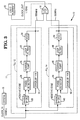
- a computer system 10 which includes a phase-locked loop (PLL) circuit 11, a crystal 18, and logic element 22.
- PLL phase-locked loop
- the PLL circuit 11 provides a signal CLOCK_OUT to the logic element 22.
- the crystal 18 provides a signal CLOCK_IN to the PLL circuit 11.
- the logic element 22 may be any computer component that requires a clock signal.
- the PLL circuit 11 includes a PLL sub-circuit 12, a PLL sub-circuit 14, and an exclusive-OR gate 16.
- the PLL sub-circuit 12 includes a divide-by-2N circuit 20, a phase detector 24, a charge pump 26, a loop filter 28, a voltage-controlled oscillator (VCO) 30, and a divide-by-11N circuit 32.
- the individual functions of the components 20, 24, 26, 28, 30, and 32 are well-known in the art.
- the PLL sub-circuit 14 includes a divide-by-2N circuit 40, a phase detector 44, a charge pump 46, a loop filter 48, a delay circuit 50, and a divide-by-11N circuit 52.
- the individual functions of components 40, 44, 46, 48, 50, and 52 are also well-known in the art.
- the PLL sub-circuit 14 acts as a slave PLL circuit to the PLL sub-circuit 12.
- the PLL sub-circuit therefore acts as a master PLL circuit.
- the PLL sub-circuit 12 feeds the signal at node C to node D of the PLL sub-circuit 14 by way of a delay line connection 56.
- the ratio 2:11 reflected in the divide-by-2N circuits 20 and 40, and the divide-by-11N circuits 32 and 52, is arbitrarily chosen based on a CLOCK_IN signal frequency of 100 MHz and an output frequency at nodes C and D of the master and slave PLL circuits 12 and 14 of 550 MHz.
- the present invention can readily employ other ratios for other frequency constraints.
- a ratio of 2:10 with a 100 MHz CLOCK_IN signal produces a frequency of 500 MHz at nodes C and D, and a CLOCK_OUT signal frequency of 1.0 GHz.
- the multiplier N can be any number, but is preferably equal to one.
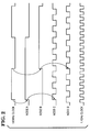
- the master PLL sub-circuit 12 is triggered by a positive clock edge from the crystal 18, while the slave PLL 14 is triggered by a negative clock edge from crystal 18.
- the multiplier N equal to one
- the output frequencies at nodes A and B of the divide-by-2N circuits 20 and 40, respectively is 50 MHz.
- the signals at nodes A and B are also ninety degrees apart in phase.
- the divide-by-llN circuit increases the 50 MHz frequency at node A to 550 MHz at node C.
- the delay circuit 50 feeds the 550 MHz signal at node C to node D over the delay circuit connection 56 (Fig. 1).
- the signal at node D is locked to the 50 MHz signal at node B, which is phase-shifted one-hundred and eighty degrees from the signal at node A.
- a phase difference of ninety degrees for the signals at nodes C and D is maintained.
- the delay circuit 50 and delay circuit connection 56 of Fig. 1 may be replaced at greater cost by another voltage-controlled oscillator 54.
- N there is no master/slave relationship between the PLL sub-circuit 12 and the PLL sub-circuit 14.
- the divide-by-llN circuits increase the 50 MHz frequency at nodes A and B to 550 MHz at nodes C and D respectively.
- the signals at nodes C and D are coupled to the exclusive-OR gate 16. Due to the ninety degree phase difference between the signals at nodes C and D, the exclusive-OR gate 16 is able to produce a CLOCK_OUT signal having double the frequency, or 1.1 GHz.
Landscapes
- Stabilization Of Oscillater, Synchronisation, Frequency Synthesizers (AREA)
Applications Claiming Priority (2)
| Application Number | Priority Date | Filing Date | Title |
|---|---|---|---|
| US329367 | 1994-10-26 | ||
| US08/329,367 US5675620A (en) | 1994-10-26 | 1994-10-26 | High-frequency phase locked loop circuit |
Publications (2)
| Publication Number | Publication Date |
|---|---|
| EP0709967A1 true EP0709967A1 (fr) | 1996-05-01 |
| EP0709967B1 EP0709967B1 (fr) | 2000-03-15 |
Family
ID=23285064
Family Applications (1)
| Application Number | Title | Priority Date | Filing Date |
|---|---|---|---|
| EP95307559A Expired - Lifetime EP0709967B1 (fr) | 1994-10-26 | 1995-10-24 | Boucle à verrouillage de phase |
Country Status (5)
| Country | Link |
|---|---|
| US (1) | US5675620A (fr) |
| EP (1) | EP0709967B1 (fr) |
| JP (1) | JP3919247B2 (fr) |
| KR (1) | KR100362841B1 (fr) |
| DE (1) | DE69515591T2 (fr) |
Cited By (1)
| Publication number | Priority date | Publication date | Assignee | Title |
|---|---|---|---|---|
| WO2001028100A1 (fr) * | 1999-10-12 | 2001-04-19 | Teradyne, Inc. | Boucle a phase asservie a faible gigue avec commande de cycle de service |
Families Citing this family (21)
| Publication number | Priority date | Publication date | Assignee | Title |
|---|---|---|---|---|
| JP3350349B2 (ja) * | 1995-09-26 | 2002-11-25 | 株式会社日立製作所 | ディジタル情報信号再生回路及びディジタル情報装置 |
| KR100206476B1 (ko) * | 1997-03-20 | 1999-07-01 | 윤종용 | 디지털 마이크로웨이브 시스템에서 송신용 국부발진주파수를 동기화시키기 위한 회로 |
| JP3313631B2 (ja) * | 1997-11-05 | 2002-08-12 | 日本電気株式会社 | 集積回路 |
| US6052034A (en) * | 1998-06-24 | 2000-04-18 | Industrial Technology Research Institute | Method and apparatus for all digital holdover circuit |
| US6594330B1 (en) * | 1999-10-26 | 2003-07-15 | Agere Systems Inc. | Phase-locked loop with digitally controlled, frequency-multiplying oscillator |
| KR100748489B1 (ko) * | 2000-01-07 | 2007-08-13 | 엘지전자 주식회사 | 디지탈 티브이의 문자 표시 장치 |
| KR100366618B1 (ko) * | 2000-03-31 | 2003-01-09 | 삼성전자 주식회사 | 클럭 신호의 듀티 사이클을 보정하는 지연 동기 루프 회로및 지연 동기 방법 |
| JP4573007B2 (ja) * | 2000-07-13 | 2010-11-04 | エルピーダメモリ株式会社 | Dll回路、及び、dll制御方法 |
| US7010077B1 (en) * | 2000-11-20 | 2006-03-07 | Agere Systems Inc. | Gated clock recovery circuit |
| KR100424180B1 (ko) * | 2001-12-21 | 2004-03-24 | 주식회사 하이닉스반도체 | 듀티 사이클 보상 기능을 갖는 지연 고정 루프 회로 |
| KR100451582B1 (ko) * | 2002-01-04 | 2004-10-08 | 엘지전자 주식회사 | Osd 폰트 전송 방법 |
| KR100885570B1 (ko) * | 2002-03-27 | 2009-02-24 | 엘지전자 주식회사 | 텔레비전 수상기 및 osd 구현방법 |
| US6774689B1 (en) | 2002-05-23 | 2004-08-10 | Cypress Semiconductor Corp. | Triple input phase detector and methodology for setting delay between two sets of phase outputs |
| US6657466B1 (en) * | 2002-05-23 | 2003-12-02 | Cypress Semiconductor Corp. | System and method for generating interleaved multi-phase outputs from a nested pair of phase locked loops |
| JP2004253056A (ja) * | 2003-02-20 | 2004-09-09 | Sanyo Electric Co Ltd | デコード装置 |
| US6960943B1 (en) * | 2003-06-06 | 2005-11-01 | Kim Alt Poulson | Suppressed micro phonic phase stable synthesizer |
| US20050062547A1 (en) * | 2003-09-22 | 2005-03-24 | Yossi Reuven | Method and apparatus to generate signals using two or more phase locked loops |
| JP4549958B2 (ja) * | 2005-02-09 | 2010-09-22 | パナソニック株式会社 | 遅延ロックドループ回路 |
| JP2007124508A (ja) * | 2005-10-31 | 2007-05-17 | Matsushita Electric Ind Co Ltd | Pll過渡応答制御システム及び通信システム |
| US8004332B2 (en) * | 2009-11-03 | 2011-08-23 | Advantest Corporation | Duty ratio control apparatus and duty ratio control method |
| KR102282954B1 (ko) * | 2021-01-20 | 2021-07-27 | 국방과학연구소 | 광대역 주파수 합성기 및 불요 신호 개선 방법 |
Citations (5)
| Publication number | Priority date | Publication date | Assignee | Title |
|---|---|---|---|---|
| US3893042A (en) * | 1973-12-12 | 1975-07-01 | Us Navy | Lock indicator for phase-locked loops |
| US4121172A (en) * | 1977-11-14 | 1978-10-17 | Magnetic Peripherals Inc. | Dual loop phase locked oscillator system |
| DE3400289A1 (de) * | 1984-01-05 | 1985-07-18 | Siemens AG, 1000 Berlin und 8000 München | Taktgenerator |
| EP0366326A2 (fr) * | 1988-10-28 | 1990-05-02 | Hewlett-Packard Company | Dispositif pour un système de distribution d'horloge à faible décalage et génération de signaux d'horloge à fréquence double |
| FR2662875A1 (fr) * | 1990-05-31 | 1991-12-06 | Bosch Gmbh Robert | Circuit d'accord avec boucle a regulation de phase et boucle a regulation de frequence. |
Family Cites Families (22)
| Publication number | Priority date | Publication date | Assignee | Title |
|---|---|---|---|---|
| FR662875A (fr) * | 1928-10-24 | 1929-08-13 | Appareil détendeur et régulateur de pression hydraulique | |
| US3621452A (en) * | 1969-11-20 | 1971-11-16 | Farinon Electric | Phase detector and oscillator system |
| US3832713A (en) * | 1973-03-01 | 1974-08-27 | Us Navy | Microwave phase shifting apparatus |
| US3849721A (en) * | 1973-08-23 | 1974-11-19 | Schlumberger Technology Corp | Microwave logging apparatus having dual processing channels |
| US4368437A (en) * | 1977-03-07 | 1983-01-11 | Wavetek Indiana, Inc. | Wide frequency range signal generator including plural phase locked loops |
| US4072905A (en) * | 1977-03-09 | 1978-02-07 | Rca Corporation | Wide acquisition range MSK demodulator input circuit |
| US4234852A (en) * | 1978-11-15 | 1980-11-18 | Mccorkle John W | Coherent frequency shift key demodulator |
| GB2045556B (en) * | 1979-03-06 | 1983-08-03 | Racal Dana Instr Ltd | Frequency synthesizers |
| US4234929A (en) * | 1979-09-24 | 1980-11-18 | Harris Corporation | Control device for a phase lock loop vernier frequency synthesizer |
| US4298986A (en) * | 1979-12-26 | 1981-11-03 | General Electric Company | Receiver for phase-shift modulated carrier signals |
| FR2544676B1 (fr) * | 1983-04-20 | 1985-12-20 | Abadie Lab | Rampe lumineuse pour l'eclairage de tableaux de bord, notamment sur avions ou helicopteres |
| US4539531A (en) * | 1983-09-26 | 1985-09-03 | Northern Telecom Limited | Phase locked loop variable oscillator with switched capacitors |
| US4814727A (en) * | 1987-12-18 | 1989-03-21 | Unisys Corporation | Wide-deviation tracking filter circuit |
| JPH02244820A (ja) * | 1989-03-16 | 1990-09-28 | Oki Electric Ind Co Ltd | Pll回路 |
| US5124569A (en) * | 1990-10-18 | 1992-06-23 | Star Technologies, Inc. | Digital phase-lock loop system with analog voltage controlled oscillator |
| US5059926A (en) * | 1991-03-13 | 1991-10-22 | Motorola, Inc. | Frequency synchronization apparatus |
| JPH04313917A (ja) * | 1991-03-29 | 1992-11-05 | Mitsubishi Electric Corp | ダブルpll装置 |
| US5299237A (en) * | 1991-12-20 | 1994-03-29 | Honeywell Inc. | Asymmetrical data tracking digital phase locked loop |
| GB2264597B (en) * | 1992-02-29 | 1995-05-10 | Nec Corp | Frequency synthesizer and method of operation |
| US5237290A (en) * | 1992-05-08 | 1993-08-17 | At&T Bell Laboratories | Method and apparatus for clock recovery |
| US5258877A (en) * | 1992-04-16 | 1993-11-02 | Vtc Inc. | Data separator having a restart circuit |
| JPH06112817A (ja) * | 1992-09-25 | 1994-04-22 | Fujitsu Ltd | Pll 周波数シンセサイザ回路 |
-
1994
- 1994-10-26 US US08/329,367 patent/US5675620A/en not_active Expired - Lifetime
-
1995
- 1995-10-23 JP JP27412295A patent/JP3919247B2/ja not_active Expired - Lifetime
- 1995-10-24 EP EP95307559A patent/EP0709967B1/fr not_active Expired - Lifetime
- 1995-10-24 DE DE69515591T patent/DE69515591T2/de not_active Expired - Lifetime
- 1995-10-25 KR KR1019950037057A patent/KR100362841B1/ko not_active Expired - Lifetime
Patent Citations (5)
| Publication number | Priority date | Publication date | Assignee | Title |
|---|---|---|---|---|
| US3893042A (en) * | 1973-12-12 | 1975-07-01 | Us Navy | Lock indicator for phase-locked loops |
| US4121172A (en) * | 1977-11-14 | 1978-10-17 | Magnetic Peripherals Inc. | Dual loop phase locked oscillator system |
| DE3400289A1 (de) * | 1984-01-05 | 1985-07-18 | Siemens AG, 1000 Berlin und 8000 München | Taktgenerator |
| EP0366326A2 (fr) * | 1988-10-28 | 1990-05-02 | Hewlett-Packard Company | Dispositif pour un système de distribution d'horloge à faible décalage et génération de signaux d'horloge à fréquence double |
| FR2662875A1 (fr) * | 1990-05-31 | 1991-12-06 | Bosch Gmbh Robert | Circuit d'accord avec boucle a regulation de phase et boucle a regulation de frequence. |
Cited By (2)
| Publication number | Priority date | Publication date | Assignee | Title |
|---|---|---|---|---|
| WO2001028100A1 (fr) * | 1999-10-12 | 2001-04-19 | Teradyne, Inc. | Boucle a phase asservie a faible gigue avec commande de cycle de service |
| US6356129B1 (en) | 1999-10-12 | 2002-03-12 | Teradyne, Inc. | Low jitter phase-locked loop with duty-cycle control |
Also Published As
| Publication number | Publication date |
|---|---|
| EP0709967B1 (fr) | 2000-03-15 |
| KR100362841B1 (ko) | 2003-02-07 |
| JP3919247B2 (ja) | 2007-05-23 |
| KR960016151A (ko) | 1996-05-22 |
| DE69515591D1 (de) | 2000-04-20 |
| DE69515591T2 (de) | 2000-09-21 |
| JPH08228151A (ja) | 1996-09-03 |
| US5675620A (en) | 1997-10-07 |
Similar Documents
| Publication | Publication Date | Title |
|---|---|---|
| EP0709967B1 (fr) | Boucle à verrouillage de phase | |
| US5359727A (en) | Clock generator using PLL and information processing system using the clock generator | |
| US6285225B1 (en) | Delay locked loop circuits and methods of operation thereof | |
| CA2251378C (fr) | Boucle a phase asservie a grande vitesse et haute precision | |
| US5699020A (en) | Phase latched differential charge pump circuit and method | |
| US6844765B2 (en) | Multi-phase clock generation circuit | |
| US5517147A (en) | Multiple-phase clock signal generator for integrated circuits, comprising PLL, counter, and logic circuits | |
| US5230013A (en) | PLL-based precision phase shifting at CMOS levels | |
| Kim et al. | A 120-MHz–1.8-GHz CMOS DLL-based clock generator for dynamic frequency scaling | |
| US6538516B2 (en) | System and method for synchronizing multiple phase-lock loops or other synchronizable oscillators without using a master clock signal | |
| EP1537669A1 (fr) | Boucle a phase asservie | |
| WO1998036491A1 (fr) | Multiplicateur de frequence d'oscillateur en anneau commande en tension | |
| US20060082399A1 (en) | Combined phase comparator and charge pump circuit | |
| CN110365330B (zh) | 一种基于fir滤波器的半数字锁相环 | |
| US6707327B2 (en) | Frequency dividing circuit | |
| JP4015254B2 (ja) | ロック検出回路及びpll周波数シンセサイザ | |
| US6466065B1 (en) | Prescaler and PLL circuit | |
| US7151398B2 (en) | Clock signal generators having programmable full-period clock skew control | |
| US6977539B1 (en) | Clock signal generators having programmable full-period clock skew control and methods of generating clock signals having programmable skews | |
| Snehalatha et al. | Comparative Analysis of Phase Locked Loop with Different Phase Frequency Detectors using 90nm Technology | |
| US5017801A (en) | Method and apparatus for converting a gap-infested read-in clock into a gap-free read-out clock | |
| US20020084816A1 (en) | Precision phase generator | |
| JPS6058609B2 (ja) | デイジタル型位相比較器 | |
| JPH02230821A (ja) | クロック発生装置及び周波数―電流変換回路 | |
| US20040113704A1 (en) | [phase lock loop circuit and operation method thereof] |
Legal Events
| Date | Code | Title | Description |
|---|---|---|---|
| PUAI | Public reference made under article 153(3) epc to a published international application that has entered the european phase |
Free format text: ORIGINAL CODE: 0009012 |
|
| AK | Designated contracting states |
Kind code of ref document: A1 Designated state(s): DE FR GB |
|
| 17P | Request for examination filed |
Effective date: 19960603 |
|
| RAP1 | Party data changed (applicant data changed or rights of an application transferred) |
Owner name: SYMBIOS, INC. |
|
| RAP1 | Party data changed (applicant data changed or rights of an application transferred) |
Owner name: HYUNDAI ELECTRONICS AMERICA |
|
| 17Q | First examination report despatched |
Effective date: 19990216 |
|
| GRAG | Despatch of communication of intention to grant |
Free format text: ORIGINAL CODE: EPIDOS AGRA |
|
| GRAG | Despatch of communication of intention to grant |
Free format text: ORIGINAL CODE: EPIDOS AGRA |
|
| GRAH | Despatch of communication of intention to grant a patent |
Free format text: ORIGINAL CODE: EPIDOS IGRA |
|
| GRAH | Despatch of communication of intention to grant a patent |
Free format text: ORIGINAL CODE: EPIDOS IGRA |
|
| GRAA | (expected) grant |
Free format text: ORIGINAL CODE: 0009210 |
|
| AK | Designated contracting states |
Kind code of ref document: B1 Designated state(s): DE FR GB |
|
| REF | Corresponds to: |
Ref document number: 69515591 Country of ref document: DE Date of ref document: 20000420 |
|
| ET | Fr: translation filed | ||
| PLBE | No opposition filed within time limit |
Free format text: ORIGINAL CODE: 0009261 |
|
| STAA | Information on the status of an ep patent application or granted ep patent |
Free format text: STATUS: NO OPPOSITION FILED WITHIN TIME LIMIT |
|
| 26N | No opposition filed | ||
| REG | Reference to a national code |
Ref country code: GB Ref legal event code: IF02 |
|
| REG | Reference to a national code |
Ref country code: GB Ref legal event code: 732E |
|
| REG | Reference to a national code |
Ref country code: FR Ref legal event code: TP |
|
| REG | Reference to a national code |
Ref country code: GB Ref legal event code: 732E |
|
| REG | Reference to a national code |
Ref country code: GB Ref legal event code: 732E |
|
| REG | Reference to a national code |
Ref country code: GB Ref legal event code: 732E |
|
| REG | Reference to a national code |
Ref country code: FR Ref legal event code: TP |
|
| PGFP | Annual fee paid to national office [announced via postgrant information from national office to epo] |
Ref country code: DE Payment date: 20141029 Year of fee payment: 20 Ref country code: GB Payment date: 20141027 Year of fee payment: 20 Ref country code: FR Payment date: 20141017 Year of fee payment: 20 |
|
| REG | Reference to a national code |
Ref country code: DE Ref legal event code: R071 Ref document number: 69515591 Country of ref document: DE |
|
| REG | Reference to a national code |
Ref country code: GB Ref legal event code: PE20 Expiry date: 20151023 |
|
| PG25 | Lapsed in a contracting state [announced via postgrant information from national office to epo] |
Ref country code: GB Free format text: LAPSE BECAUSE OF EXPIRATION OF PROTECTION Effective date: 20151023 |