EP0720103A1 - Circuit de calcul d'un bidimensionnel transformé discrète inverse du cosinus - Google Patents
Circuit de calcul d'un bidimensionnel transformé discrète inverse du cosinus Download PDFInfo
- Publication number
- EP0720103A1 EP0720103A1 EP94120917A EP94120917A EP0720103A1 EP 0720103 A1 EP0720103 A1 EP 0720103A1 EP 94120917 A EP94120917 A EP 94120917A EP 94120917 A EP94120917 A EP 94120917A EP 0720103 A1 EP0720103 A1 EP 0720103A1
- Authority
- EP
- European Patent Office
- Prior art keywords
- idct
- matrix
- data
- input data
- input
- Prior art date
- Legal status (The legal status is an assumption and is not a legal conclusion. Google has not performed a legal analysis and makes no representation as to the accuracy of the status listed.)
- Withdrawn
Links
Images



Classifications
-
- G—PHYSICS
- G06—COMPUTING OR CALCULATING; COUNTING
- G06F—ELECTRIC DIGITAL DATA PROCESSING
- G06F17/00—Digital computing or data processing equipment or methods, specially adapted for specific functions
- G06F17/10—Complex mathematical operations
- G06F17/14—Fourier, Walsh or analogous domain transformations, e.g. Laplace, Hilbert, Karhunen-Loeve, transforms
- G06F17/147—Discrete orthonormal transforms, e.g. discrete cosine transform, discrete sine transform, and variations therefrom, e.g. modified discrete cosine transform, integer transforms approximating the discrete cosine transform
Definitions
- the present invention relates to a circuit for performing a two-dimensional inverse discrete cosine transform(IDCT); and, more particularly, to a two-dimensional IDCT circuit which uses a pair of improved one-dimensional IDCT circuits wherein each of the circuits performs an IDCT operation by using a matrix multiplication.
- IDCT two-dimensional inverse discrete cosine transform
- transmission of digitized video signals can deliver video images of much higher quality than the transmission of analog signals.
- an image signal comprising a sequence of image "frames"
- a substantial amount of data is generated for transmission, especially in the case of a high definition television system. Since, however, the available frequency bandwidth of a conventional transmission channel is limited, in order to transmit the substantial amounts of digital data through the limited channel bandwidth, it is inevitable to compress or reduce the volume of the transmission data.
- the image signal can be normally compressed without seriously affecting its integrity because there usually exist certain correlationships or redundancies among some of the pixels in a single frame and also among those of neighboring frames. Accordingly, most of prior art image signal encoding methods employ various compression techniques (or coding methods) built on the idea of utilizing or truncating the redundancies.
- DCT Discrete Cosine Transform
- a square block of digitally encoded pixels can be transformed into the frequency domain by means of a two-dimensional or NxN DCT processor for performing the two-dimensional DCT by a row-column decomposition method, wherein the NxN block of pixel data is inputted thereto, the input matrix is multiplied by an NxN DCT matrix to yield an intermediate matrix, and then the transpose of the intermediate matrix is multiplied by the same DCT matrix to yield the desired inverse transformed matrix.
- the elements of the transformed matrix can then be quantized and only the most energetic terms therein are selected for transmission.
- an inverse discrete cosine transform IDCT
- IDCT inverse discrete cosine transform
- Matrix multiplication involves forming the inner products of two N dimensional vectors to yield a single element of the product matrix.
- each element in a row of the input matrix is multiplied by each of the corresponding elements of a column of the DCT/IDCT matrix and the products are summed to yield a single element of the product matrix.
- 8 products are summed to yield a single element of the output matrix which has 64 elements.
- Many fast algorithms have been derived to reduce the number of computations required. For example, the DCT/IDCT matrix is decomposed into several sparse matrices, which result in butterfly structures.
- U. S. Patent No. 4,791,598 issued to M. L Niou et al. provides another DCT/IDCT scheme involving a distributed arithmetic combined with decimation-in-frequency, bit-serial structures, and partial sums to implement vector inner products concurrently with a minimal memory size.
- the result is an architecture with a highly regular structure and no multipliers.
- This is possible because of the inherent properties of the transform operations: namely, the elements in the transform matrix are constants which permits the use of distributed arithmetic wherein memory lookup tables, or Read Only Memories(ROMs), are used as a substitute for multipliers; and the matrix-vector products are realized by several concurrent vector inner products.
- This scheme is efficient in that it has no multipliers and uses a highly regulated structure.
- a primary object of the present invention to provide a high speed IDCT circuit with a reduced hardware complexity which is applicable to a real time image processing system, wherein Programmable Logic Arrays (PLAs) are employed for the matrix multiplication performed in the IDCT operation.
- PLAs Programmable Logic Arrays
- a one-dimensional Inverse Discrete Cosine Transform (IDCT) circuit for performing an IDCT operation on N input data to thereby provide N output data, wherein said N input data consists of N/2 odd-numbered input data and N/2 even-numbered input data, comprising: first multiplication means for performing a predetermined even IDCT matrix multiplication on said even-numbered input data, thereby providing a first set of N/2 intermediate data, wherein said first means includes a plurality of multipliers and a multiplicity of adders to perform the even IDCT matrix multiplication on the N/2 even-numbered input data; second multiplication means for performing a predetermined odd IDCT matrix multiplication on said odd-numbered input data, thereby providing a second set of N/2 intermediate data, wherein said second means includes a host of multipliers and a multitude of adders to perform the odd IDCT matrix multiplication on the N/2 odd-numbered input data; addition means for adding each of the first set of N/2 intermediate data to each corresponding data of the second set of intermediate data
- N dimensional input vector is first divided into N/2 dimensional even-numbered input vector, e.g., (y0, y2, y4, y6), and odd-numbered input vector, e.g., (y1, y3, y5, y7).
- An even IDCT matrix of Eq. (9a) is multiplied with the even-numbered input vector to provide N/2 intermediate data, each of which is a sum of two elements of the output vector.
- the odd-numbered input vector is multiplied with an odd IDCT matrix of Eq. (9b), to thereby provide another N/2 intermediate data, each of which is a difference of two elements of the output vector.
- a prior art IDCT processor performs IDCT operation based on Eqs. (9a) and (9b), using the distributed arithmetic and bit serial data structure( see U. S. Patent No. 4,791,598 issued to M. L Niou et al.).
- FIG. 1 there is a block diagram showing an IDCT circuit which performs the one-dimensional IDCT operation of Eqs. (10a) to (10c).
- An even IDCT block 100 performs the multiplication of the even IDCT matrix shown in Eq. (9a) while an odd IDCT block 200 performs the multiplication of the odd IDCT matrix shown in Eq. (9b). From Eqs. (9a) and (9b), it can be easily recognized that the two IDCT blocks 100 and 200 can be implemented in a same manner.
- An input vector which is a row of an input matrix, is first separated into even-numbered and odd-numbered input vectors and fed to the even and odd IDCT blocks 100 and 200, respectively.
- N 8
- the input vector (y0, y1, y2, ... y7) is separated into (y0, y2, y4, y6) and (y1, y3, y5, y7); and a pair of input data, e.g., (y0, y1), is inputted on lines IN_EVEN and IN_ODD at a same clock cycle.
- the even-numbered input vector of Eqs. (10a) and (10b) is first sequentially fed to and stored in a register and latch block 111, and then outputted in parallel.
- the input vector is latched on the output port of the register and latch block 111 for 4 clock cycles.
- y2 and y6 are dispatched to multipliers 141 and 142, via a multiplexor(MUX) 122 for the computation of Eq. (10b).
- y0 and y4 are provided on line 113 and to a 2's complement converter 121, respectively, for the computation of Eq. (10a).
- multipliers 141 and 142 there are two multipliers, i.e., MUL(c2) 141 and MUL(c6) 142, in the even IDCT block 100 for performing the matrix multiplication of Eq. (10b).
- the calculated results from the multipliers 141 and 142 are fed to an adder 152.
- C4 in Eq. (10a) is 1 and need not be multiplied to the input data, e.g., y0 and y4 in Eq. (10a). Therefore, y0 is fed to an adder 151 directly and y4 is fed to the adder 151 via the 2's complement converter 121.
- the data processed herein is represented in a 2's complement form and the 2's complement converter 121 may convert the sign of the y4 for the computation of Eq. (10a) in response to COEF_SIGN, i.e., the signal which denotes the sign of an element in the reduced IDCT matrices.
- COEF_SIGN the signal which denotes the sign of an element in the reduced IDCT matrices.
- Table 1 The operations of two multipliers 141 and 142 and the data provided on lines 113 and 114 are depicted in Table 1.
- Each row in Table 1 shows 4 input data to adders 151 and 152 at each clock cycle.
- the adder 151 adds two elements from the 4th and the 5th columns in a same row in each clock cycle, while the adder 152 adds those from the 2nd and the 3rd columns of Table 1.
- the results from the two adders 151 and 152 are fed to the adder/subtractor 161 wherein the 4 elements in a row in Table 1 are added altogether.
- the result of adder 152 is subtracted from that of adder 151 at the adder/subtractor 161.
- the outputs of the adders 151 and 152 is same as the results of Eqs. (10a) and (10b) and the output of the adder/subtractor 161 is same as the result of Eq. (9a).
- the same operation is performed twice in the multipliers 141 and 142 and adders 151 and 152 to provide the desired result at the adder/subtractor 161.
- the even IDCT block 100 performs the operation of multiplying the even IDCT matrix with the even-numbered input vector as shown in Eq. (9a).
- the overall operation of the odd IDCT block 200 is similar to that of the even IDCT block 100, except that 4 multipliers are needed for c1, c3, c5 and c7 of Eq. (10c).
- the odd-numbered input vector is latched on the output port of a register and latch block 112 for 4 clock cycles and dispatched to the four multipliers 143 to 146 via a multiplexor 123 for the computation of Eq. (10c).
- Table 3 the operations of the four multipliers 143 to 146 at different clock cycles are presented.
- Table 3 clock cycle MUL(c1) MUL(c3) MUL(c5) MUL(c7) 1 c1 x y1 c3 x y3 c5 x y5 c7 x y7 2 -c1 x y5 c3 x y1 -c5 x y7 -c7 x y3 3 -c1 x y3 c3 x y7 c5 x y1 c7 x y5 4 -c1 x y7 c3 x y5 -c5 x y3 c7 x y1
- the four components in each row are added in 3 adders 153, 154 and 162 at a corresponding clock cycle, thereby providing each element of the left part of Eq. (10c).
- the odd IDCT block 200 multiplies the odd IDCT matrix with the odd-numbered input vector
- the results of adder/subtractor 161 and adder 162 as presented by Eqs. (9a) and (9b) are added and subtracted at an adder 171 and a subtractor 172, respectively, to thereby provide the output data, e.g., x0 to x7.
- 4 pairs of results e.g. (x0, x7), (x1,x6), (x2, x5) and (x3, x4), are provided sequentially with the first component from the adder 171 and the second component from the subtractor 172, respectively.
- the results are provided sequentially one at a time and are rounded or clipped to predetermined bits at round/clip blocks 181 and 182, considering the dynamic range of the data processed in the system.
- next input vector i.e., another row of the NxN input matrix. While an input vector is latched on the output port of the register and latch blocks 111 and 112, a next input vector is inputted thereto, thereby enabling the processing of the subsequent input vector without stopping.
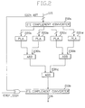
- the multiplier includes 2's compliment converters 210a and 210b, PLAs 220a to 220d and adders 230a to 230c.
- y2 or y6 of Eq. (10b) is inputted to MUL(c2) 141 on line 115 shown in Fig. 1.
- the four PLAs 220a to 220d and the 3 adders 230a to 230c perform a multiplication operation between two positive numbers, i.e., the absolute value of the input data and the predetermined multiplication coefficient which is one element, e.g., c2, of the IDCT matrices shown in Eqs. (10a) to (10c).
- the input is a negative number which is represented in a 2's complement form
- it is first converted to a corresponding positive number at the first 2's complement converter 210a.
- An MSB (Most Significant Bit) or sign bit of the input is fed as SIGN BIT to the 2's complement converter 210a to determine whether the converting should take place therein.
- the output from the 2's complement converter 210a is split into a multiplicity of, e.g., 4, groups of bits.
- Each of the PLAs receives each group of bits and provides a partial result of the multiplication corresponding to the group of input bits, wherein the partial result is the multiplication coefficient multiplied by the input bits.
- the structures of the PLAs can be predetermined based on the number of bits of the input and the multiplication coefficient. Specifically, one PLA includes all partial results for all the possible input bits and performs the multiplication operation by selecting one of the predetermined partial results in response to the input bits thereto.
- the four partial results from the four PLAs 220a to 220d are shifted and added at the adders 230a to 230c, to thereby provide a complete multiplied result.
- the sign of the multiplied result is determined. Specifically, if the input is positive and the multiplication coefficient is positive as in the 1st and 4th clock cycles of the 2nd column of Table 2, the result of adder 230c is provided as the output of MUL(c2) on line 116 shown in Fig. 1. In case both are negative, the result is the same. Otherwise, i.e., if one and only one of them is negative, the output of MUL(c2) is converted to the corresponding negative number at the second 2's complement converter 210b.
- Signals SIGN BIT and COEF_SIGN which represent the sign of the input data and the multiplication coefficient, are inputted to the 2's complement converter 210b via an XOR(exclusive OR) gate to enable the above operation.
- the 2's complement converters 210a and 210b may also comprise PLAs to perform the conversion efficiently.
- the multipliers 141 to 146 shown in Fig. 1 perform the multiplication assigned in Tables 2 and 3 in a more efficient manner than the prior art methods which are based on the distributed arithmetic and bit-serial data structure.
- the detailed structure of the multiplier may vary depending on the number of bits of the input thereto and the multiplication coefficient, but its main structure remains similar to that of Fig. 2.
- IDCT is performed on an input matrix, i.e., two-dimensional DCT transformed data.
- a two-dimensional IDCT circuit can be constructed by using a pair of one-dimensional IDCT circuits described above.
- FIG. 3 there is shown an IDCT circuit of the present invention to perform the calculation of Eq. (13).
- the circuitry of Fig. 3 has a first 1-D (one-dimensional) IDCT circuit 310 for performing the IDCT matrix multiplication on an NxN input matrix to thereby provide an intermediate matrix, a transposition memory 320 for transposing the intermediate matrix, a second 1-D IDCT circuit 330 for subjecting the transposed intermediate matrix to another IDCT matrix multiplication, and a controller 340 for generating various control signals used in the IDCT circuit of the present invention.
- the two 1-D IDCT circuits 310 and 330 are designed as explained in reference to Figs. 1 and 2. Therefore, a pair of input data, one of which is odd-numbered and the other is even-numbered, is inputted to the first 1-D IDCT circuit 310 at a same clock cycle, and a pair of elements of the intermediate matrix is provided in the manner explained above.
- the intermediate matrix provided from the first 1-D IDCT circuit 310 is transposed at the transposition memory 320, thereby being provided to the second 1-D IDCT circuit 330.
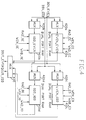
- the transposition memory 320 includes four dual port RAMs 410a to 410d each of which can accommodate 16 elements of the intermediate matrix and additional circuitry for the transposition operation.
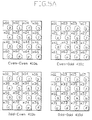
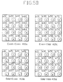
- the intermediate matrix outputted from the 1-D IDCT circuit 310 is divided into 4 sets, i.e., even-even, odd-even, even-odd and odd-odd, and stored in the corresponding dual-port RAMs 410a to 410d as depicted in Fig. 5A or Fig. 5B, wherein xij means an element of the ith row and jth column of the intermediate matrix.
- Fig. 5A or Fig. 5B wherein xij means an element of the ith row and jth column of the intermediate matrix.
- the dual-port RAM Even_Even 410a stores the data whose column and row numbers are even and the dual-port RAM Even_Odd 410c stores the data whose column number is odd and row number is even.
- the data is outputted in a different sequence from the input sequence of the intermediate matrix to the transposition memory 320.
- the intermediate matrix provided on lines OUT_EVEN and OUT_ODD in Fig. 1 is inputted on lines DIN_EVEN and DIN_ODD as shown in Table 4:
- Table 5 denote writing addresses for each of the four dual port RAMs 410a to 410d in accordance with Figs. 5A and 5B, respectively.
- x means that no data is stored in the corresponding dual-port RAM in those clock cycles.
- the data stored in the dual-port RAMs 410a to 410d in the manner of Fig. 5A or Fig. 5B is provided in a tranposed sequence to the second 1-D IDCT circuit 330 on lines DOUT_EVEN and DOUT_ODD shown in Fig. 4. While the elements of the intermediate matrix currently stored in the dual-port RAMs, 410a to 410d, are retrieved therefrom, the next intermediate matrix calculated from a next input matrix is inputted thereto. To prevent any loss of data, the read and write operation of the dual-port RAMs 410a to 410d should be designed such that new data is stored in an address wherein previously stored intermediate matrix data has been already retrieved. To transpose the intermediate matrix currently stored as Fig.
- the first column of the intermediate matrix stored in the first columns of the dual-port RAMs 410a and 410b are retrieved first.
- data of a next intermediate matrix can be written thereto in place of the retrieved data.
- First 8 data in the next block are stored in a manner of first columns of dual-port RAMs Even_Even 410a and Odd_Even 410b in Fig. 5B, to prevent the loss of the data in a currently stored intermediate matrix which remains in the second to forth columns of dual-port RAMs 410a and 410b.
- the remaining data of the next block are stored in the manner of Fig. 5B after the data stored at the corresponding position are retrieved.
- subsequent intermediate matrices are stored in the four dual-port RAMs 410a to 410d alternately, one time as shown in Fig. 5A and another time as shown in Fig. 5B.
- subsequent blocks of data can be stored and transposed in the 4 dual-port RAMs without incurring a loss of data in the transposition process.
- a block of data inputted in pairs from the first 1-D IDCT circuit 310 on lines DIN_EVEN and DIN_ODD is stored in the 4 dual-port RAMs in a manner depicted in Figs. 5A and 5B alternately by using 4 multiplexors 420a to 420d.
- a pair of elements of the intermediate matrix are provided from the dual-port RAMs 410a to 410d by way of a multiplexor 430, to thereby be coupled to the second 1-D IDCT circuit 330 shown in Fig. 3. This time the data is retrieved in a transposed sequence.
- data in a first column e.g., x00, x10, ...
- Table 6 read clock cycle DOUT_EVEN DOUT_ODD 1 - 4 x00,x60,x20,x40 x70,x10,x50,x30 5 - 8 x01,x61,x21,x41 x71,x11,x51,x31 9 - 12 x02,x62,x22,x42 x72,x12,x52,x32 . . . . . . .
- Table 7a clock 1 2 3 4 5 6 7 8 9 10 11 .. write data x00 x06 x02 x04 x10 x16 x12 x14 x20 x26 x22 .. x07 x01 x05 x03 x17 x11 x15 x13 x27 x21 x25 .. write address 0 3 1 2 0 3 1 2 4 7 5 .. 3 0 2 1 3 0 2 1 7 4 6 .. read data U U U U U U U U U U U U U U U U U U U U U U U U U U U U U U U U U U U U U U U U U U U U U U U U U U U U U U U U U U U U U U U U U U U U U U U U U U U U U U U U U U U U U U U U U U U U U U U U U U U U U U U U U U U U U U U U U U U U U U U U . ..
- a read cycle starts with a 30th write clock cycle in Table 7b to prevent a loss of data as explained above: that is, after 29x2 data of the intermediate matrix is inputted and stored in the dual-port RAMs via each input line DIN_EVEN and DIN_OUT, first 2 elements, e.g., x00 and x70, of the transposed intermediate matrix are retrieved therefrom on lines DOUT_EVEN and DOUT_ODD.
- the read and write clock cycles are determined such that data in an address is retrieved only after an element of the current intermediate matrix is written thereto, and stored data in the address is replaced by an element of a next intermediate matrix only after it is retrieved therefrom.
- x70 is written in a 29th write clock cycle and retrieved in the 1st read cycle or 30th write cycle. Sequences of addresses are generated in a timely manner to enable the read and write operation described above.
- 2 address signals e.g, read address RAD_EE and write address WAD_EE
- WEN_EE write enable input signal
- RAD_EE read address
- WEN_OE write enable input signal
- Various signals presented above e.g., RAD_EE, WEN_OE, WAD_OO, are generated using the circuitry shown in Fig. 6.
- the circuitry depicted in Fig. 6 may be incorporated in the controller 340 shown in Fig. 3.
- a read/write point signal generator 705 provides a read and a write point signals in response to a clock signal.
- the read point signal indicates a start of read operation of each intermediate matrix to the transposition memory 320, while the write point signal indicates a start of write operation for each of the intermediate matrices.
- the write point signal may be enabled at the 1st and 33th write clock cycles while the read point signal may be enabled at the 30th write clock cycle in Tables 7a and 7b.
- HOR_AD_GEN1 720a and HOR_AD_GEN2 720b generate write addresses for storing data as in Fig. 5A
- HOR_AD_GEN1 710a and HOR_AD_GEN2 710b generate read addresses for retrieving data which has been stored as in Fig. 5B
- VER_AD_GEN1 720c and VER_AD_GEN2 720d generate write addresses for storing data as in Fig.
- VER_AD_GEN1 710c and VER_AD_GEN2 720d generate read addresses for retrieving data which has been stored as in Fig. 5A.
- the read and write addresses are generated alternately on a block-by-block basis by using T flip-flops 712 and 722 and multiplexors 715a to 715d and 725a to 725d.
- the read address signals RAD_EE, RAD_EO, RAD_OE and RAD_OO, and the write address signals WAD_EE, WAD_EO, WAD_OE and WAD_OO are provided to the corresponding dual-port RAMs as shown in Fig. 4.
- write enable signals are also generated. Two of the 4 dual-port RAMs are write enabled at the same time as specified in Table 5 by using the enable signal generating circuit 740 shown in Fig. 6.
- the transposed intermediate matrix is inputted to the second 1-D IDCT circuit 330 shown in Fig. 3.
- the sequence of read data or input data to the second 1-D IDCT circuit 330 is different from the input data sequence to the 1st 1-D IDCT circuit 310.
- the data of the first intermediate matrix e.g., x00, x60, x20, x40
- the second 1-D IDCT circuit 330 performs the same operation with the first 1-D IDCT circuit 310 except that the former operates with different input data. Therefore, the second 1-D IDCT circuit 330 can also be constructed as depicted in Fig. 1.
- An input vector is sequentially inputted, stored and latched in the register and latch blocks 111 and 112 shown in Fig. 1; and, therefore, the operation of the circuitry in Fig. 1 except the register and latch blocks 111 and 112 is identical for the first and second 1-D IDCT circuits.
- the two-dimensional IDCT is achieved by transposing the result of one-dimensional IDCT and again subjecting it to one-dimensional IDCT.
Landscapes
- Physics & Mathematics (AREA)
- Engineering & Computer Science (AREA)
- General Physics & Mathematics (AREA)
- Mathematical Physics (AREA)
- Mathematical Analysis (AREA)
- Mathematical Optimization (AREA)
- Computational Mathematics (AREA)
- Pure & Applied Mathematics (AREA)
- Data Mining & Analysis (AREA)
- Theoretical Computer Science (AREA)
- Discrete Mathematics (AREA)
- Algebra (AREA)
- Databases & Information Systems (AREA)
- Software Systems (AREA)
- General Engineering & Computer Science (AREA)
- Complex Calculations (AREA)
Priority Applications (1)
| Application Number | Priority Date | Filing Date | Title |
|---|---|---|---|
| EP94120917A EP0720103A1 (fr) | 1994-12-29 | 1994-12-29 | Circuit de calcul d'un bidimensionnel transformé discrète inverse du cosinus |
Applications Claiming Priority (1)
| Application Number | Priority Date | Filing Date | Title |
|---|---|---|---|
| EP94120917A EP0720103A1 (fr) | 1994-12-29 | 1994-12-29 | Circuit de calcul d'un bidimensionnel transformé discrète inverse du cosinus |
Publications (1)
| Publication Number | Publication Date |
|---|---|
| EP0720103A1 true EP0720103A1 (fr) | 1996-07-03 |
Family
ID=8216577
Family Applications (1)
| Application Number | Title | Priority Date | Filing Date |
|---|---|---|---|
| EP94120917A Withdrawn EP0720103A1 (fr) | 1994-12-29 | 1994-12-29 | Circuit de calcul d'un bidimensionnel transformé discrète inverse du cosinus |
Country Status (1)
| Country | Link |
|---|---|
| EP (1) | EP0720103A1 (fr) |
Cited By (3)
| Publication number | Priority date | Publication date | Assignee | Title |
|---|---|---|---|---|
| WO2001035267A1 (fr) * | 1999-11-12 | 2001-05-17 | Bops, Incorporated | Procede et appareil permettant de mettre en oeuvre une transformee de cosinus efficace |
| US6754687B1 (en) | 1999-11-12 | 2004-06-22 | Pts Corporation | Methods and apparatus for efficient cosine transform implementations |
| JP2015055971A (ja) * | 2013-09-11 | 2015-03-23 | 富士通株式会社 | 積和演算回路及び積和演算システム |
Citations (6)
| Publication number | Priority date | Publication date | Assignee | Title |
|---|---|---|---|---|
| EP0376683A2 (fr) * | 1988-12-27 | 1990-07-04 | Kabushiki Kaisha Toshiba | Appareil de calcul d'une transformée discrète du cosinus |
| EP0506111A2 (fr) * | 1991-03-27 | 1992-09-30 | Mitsubishi Denki Kabushiki Kaisha | Processeur de calcul d'une transformée discrète/inverse-discrète du cosinus, et procédé de traitement de données |
| US5181183A (en) * | 1990-01-17 | 1993-01-19 | Nec Corporation | Discrete cosine transform circuit suitable for integrated circuit implementation |
| EP0575675A1 (fr) * | 1992-06-26 | 1993-12-29 | Discovision Associates | Procédé et agencement de transformation de signaux à partir d'un domaine de fréquence dans un domaine du temps |
| DE4345029A1 (de) * | 1992-12-30 | 1994-07-07 | Korea Electronics Telecomm | Schaltkreis für diskrete Kosinustransformation |
| EP0621543A2 (fr) * | 1993-04-19 | 1994-10-26 | General Instrument Corporation Of Delaware | Processeur de calcul d'une transformée discrète inverse de cosinus |
-
1994
- 1994-12-29 EP EP94120917A patent/EP0720103A1/fr not_active Withdrawn
Patent Citations (6)
| Publication number | Priority date | Publication date | Assignee | Title |
|---|---|---|---|---|
| EP0376683A2 (fr) * | 1988-12-27 | 1990-07-04 | Kabushiki Kaisha Toshiba | Appareil de calcul d'une transformée discrète du cosinus |
| US5181183A (en) * | 1990-01-17 | 1993-01-19 | Nec Corporation | Discrete cosine transform circuit suitable for integrated circuit implementation |
| EP0506111A2 (fr) * | 1991-03-27 | 1992-09-30 | Mitsubishi Denki Kabushiki Kaisha | Processeur de calcul d'une transformée discrète/inverse-discrète du cosinus, et procédé de traitement de données |
| EP0575675A1 (fr) * | 1992-06-26 | 1993-12-29 | Discovision Associates | Procédé et agencement de transformation de signaux à partir d'un domaine de fréquence dans un domaine du temps |
| DE4345029A1 (de) * | 1992-12-30 | 1994-07-07 | Korea Electronics Telecomm | Schaltkreis für diskrete Kosinustransformation |
| EP0621543A2 (fr) * | 1993-04-19 | 1994-10-26 | General Instrument Corporation Of Delaware | Processeur de calcul d'une transformée discrète inverse de cosinus |
Non-Patent Citations (2)
| Title |
|---|
| HIROSHI FUJIWARA ET AL: "An All - ASIC Implementation of a Low Bit-rate Video Codec", IEEE TRANSACTIONS ON CIRCUITS AND SYSTEMS FOR VIDEO TECHNOLOGY, vol. 2, no. 2, NEW YORK US, pages 123 - 134, XP000280652 * |
| K.W.CURRENT ET AL: "Unified forward and inverse discrete cosine transform architecture and proposed VLSI implementation", INTERNATIONAL JOURNAL OF ELECTRONICS, vol. 69, no. 2, LONDON GB, pages 233 - 246, XP000148312 * |
Cited By (3)
| Publication number | Priority date | Publication date | Assignee | Title |
|---|---|---|---|---|
| WO2001035267A1 (fr) * | 1999-11-12 | 2001-05-17 | Bops, Incorporated | Procede et appareil permettant de mettre en oeuvre une transformee de cosinus efficace |
| US6754687B1 (en) | 1999-11-12 | 2004-06-22 | Pts Corporation | Methods and apparatus for efficient cosine transform implementations |
| JP2015055971A (ja) * | 2013-09-11 | 2015-03-23 | 富士通株式会社 | 積和演算回路及び積和演算システム |
Similar Documents
| Publication | Publication Date | Title |
|---|---|---|
| EP0353223B1 (fr) | Processeur permettant d'obtenir des transformees de cosinus discretes bidimensionnelles | |
| EP0506111B1 (fr) | Processeur de calcul d'une transformée discrète/inverse-discrète du cosinus, et procédé de traitement de données | |
| JP2931389B2 (ja) | 単一のマルチプライヤ/アキュムレータと単一のランダムアクセスメモリを用いてdct/idct演算を繰り返す集積回路装置 | |
| EP0621543B1 (fr) | Processeur de calcul d'une transformée discrète inverse de cosinus | |
| US5539836A (en) | Method and apparatus for the realization of two-dimensional discrete cosine transform for an 8*8 image fragment | |
| EP0286183A1 (fr) | Système de transmission de télévision utilisant le codage par transformée | |
| US5649077A (en) | Modularized architecture for rendering scaled discrete cosine transform coefficients and inverse thereof for rapid implementation | |
| EP0720104A2 (fr) | Appareil pour la transformation discrète inverse du cosinus | |
| US5636152A (en) | Two-dimensional inverse discrete cosine transform processor | |
| CN1142162A (zh) | 二维逆离散余弦变换电路 | |
| Jang et al. | A 0.8/spl mu/100-MHz 2-D DCT core processor | |
| JPH07121507A (ja) | 離散コサイン変換装置 | |
| US20100104023A1 (en) | Compressing Video Frames | |
| KR0154919B1 (ko) | 2차원 역이산 코사인 변환 회로 | |
| Sjostrom et al. | Discrete cosine transform chip for real-time video applications | |
| Divakara et al. | Novel dwt/idwt architecture for 3d with nine stage 2d parallel processing using split distributed arithmetic | |
| JP3046115B2 (ja) | 離散コサイン変換器 | |
| JPH08194686A (ja) | 1次元および2次元逆離散的コサイン変換(idct)回路 | |
| Aroutchelvame et al. | Architecture of wavelet packet transform for 1-D signal | |
| JP3046116B2 (ja) | 離散コサイン変換器 | |
| Hsieh et al. | Implementation of an Efficient DWT Using a FPGA on a Real-time Platform | |
| JP3214831B2 (ja) | データ処理装置 | |
| JP3397838B2 (ja) | 画像処理装置及び離散コサイン変換方法 | |
| JPH0645947A (ja) | 直交変換装置及び逆直交変換装置 | |
| Chang et al. | A VLSI data compression chip for high-speed image compression |
Legal Events
| Date | Code | Title | Description |
|---|---|---|---|
| PUAI | Public reference made under article 153(3) epc to a published international application that has entered the european phase |
Free format text: ORIGINAL CODE: 0009012 |
|
| AK | Designated contracting states |
Kind code of ref document: A1 Designated state(s): DE FR GB NL |
|
| 17P | Request for examination filed |
Effective date: 19961206 |
|
| 17Q | First examination report despatched |
Effective date: 19980310 |
|
| STAA | Information on the status of an ep patent application or granted ep patent |
Free format text: STATUS: THE APPLICATION IS DEEMED TO BE WITHDRAWN |
|
| 18D | Application deemed to be withdrawn |
Effective date: 19980922 |