EP0720232A1 - Circuit multipuce - Google Patents
Circuit multipuce Download PDFInfo
- Publication number
- EP0720232A1 EP0720232A1 EP94927045A EP94927045A EP0720232A1 EP 0720232 A1 EP0720232 A1 EP 0720232A1 EP 94927045 A EP94927045 A EP 94927045A EP 94927045 A EP94927045 A EP 94927045A EP 0720232 A1 EP0720232 A1 EP 0720232A1
- Authority
- EP
- European Patent Office
- Prior art keywords
- wiring board
- printed wiring
- chip module
- bare
- chips
- Prior art date
- Legal status (The legal status is an assumption and is not a legal conclusion. Google has not performed a legal analysis and makes no representation as to the accuracy of the status listed.)
- Granted
Links
Images








Classifications
-
- H—ELECTRICITY
- H10—SEMICONDUCTOR DEVICES; ELECTRIC SOLID-STATE DEVICES NOT OTHERWISE PROVIDED FOR
- H10W—GENERIC PACKAGES, INTERCONNECTIONS, CONNECTORS OR OTHER CONSTRUCTIONAL DETAILS OF DEVICES COVERED BY CLASS H10
- H10W90/00—Package configurations
-
- H—ELECTRICITY
- H05—ELECTRIC TECHNIQUES NOT OTHERWISE PROVIDED FOR
- H05K—PRINTED CIRCUITS; CASINGS OR CONSTRUCTIONAL DETAILS OF ELECTRIC APPARATUS; MANUFACTURE OF ASSEMBLAGES OF ELECTRICAL COMPONENTS
- H05K1/00—Printed circuits
- H05K1/02—Details
- H05K1/14—Structural association of two or more printed circuits
- H05K1/141—One or more single auxiliary printed circuits mounted on a main printed circuit, e.g. modules, adapters
-
- H—ELECTRICITY
- H10—SEMICONDUCTOR DEVICES; ELECTRIC SOLID-STATE DEVICES NOT OTHERWISE PROVIDED FOR
- H10W—GENERIC PACKAGES, INTERCONNECTIONS, CONNECTORS OR OTHER CONSTRUCTIONAL DETAILS OF DEVICES COVERED BY CLASS H10
- H10W70/00—Package substrates; Interposers; Redistribution layers [RDL]
- H10W70/60—Insulating or insulated package substrates; Interposers; Redistribution layers
- H10W70/611—Insulating or insulated package substrates; Interposers; Redistribution layers for connecting multiple chips together
-
- H—ELECTRICITY
- H10—SEMICONDUCTOR DEVICES; ELECTRIC SOLID-STATE DEVICES NOT OTHERWISE PROVIDED FOR
- H10W—GENERIC PACKAGES, INTERCONNECTIONS, CONNECTORS OR OTHER CONSTRUCTIONAL DETAILS OF DEVICES COVERED BY CLASS H10
- H10W76/00—Containers; Fillings or auxiliary members therefor; Seals
- H10W76/40—Fillings or auxiliary members in containers, e.g. centering rings
- H10W76/42—Fillings
- H10W76/47—Solid or gel fillings
-
- H—ELECTRICITY
- H10—SEMICONDUCTOR DEVICES; ELECTRIC SOLID-STATE DEVICES NOT OTHERWISE PROVIDED FOR
- H10W—GENERIC PACKAGES, INTERCONNECTIONS, CONNECTORS OR OTHER CONSTRUCTIONAL DETAILS OF DEVICES COVERED BY CLASS H10
- H10W90/00—Package configurations
- H10W90/401—Package configurations characterised by multiple insulating or insulated package substrates, interposers or RDLs
-
- H—ELECTRICITY
- H05—ELECTRIC TECHNIQUES NOT OTHERWISE PROVIDED FOR
- H05K—PRINTED CIRCUITS; CASINGS OR CONSTRUCTIONAL DETAILS OF ELECTRIC APPARATUS; MANUFACTURE OF ASSEMBLAGES OF ELECTRICAL COMPONENTS
- H05K1/00—Printed circuits
- H05K1/02—Details
- H05K1/14—Structural association of two or more printed circuits
- H05K1/147—Structural association of two or more printed circuits at least one of the printed circuits being bent or folded, e.g. by using a flexible printed circuit
-
- H—ELECTRICITY
- H05—ELECTRIC TECHNIQUES NOT OTHERWISE PROVIDED FOR
- H05K—PRINTED CIRCUITS; CASINGS OR CONSTRUCTIONAL DETAILS OF ELECTRIC APPARATUS; MANUFACTURE OF ASSEMBLAGES OF ELECTRICAL COMPONENTS
- H05K2201/00—Indexing scheme relating to printed circuits covered by H05K1/00
- H05K2201/09—Shape and layout
- H05K2201/09145—Edge details
- H05K2201/09181—Notches in edge pads
-
- H—ELECTRICITY
- H05—ELECTRIC TECHNIQUES NOT OTHERWISE PROVIDED FOR
- H05K—PRINTED CIRCUITS; CASINGS OR CONSTRUCTIONAL DETAILS OF ELECTRIC APPARATUS; MANUFACTURE OF ASSEMBLAGES OF ELECTRICAL COMPONENTS
- H05K2201/00—Indexing scheme relating to printed circuits covered by H05K1/00
- H05K2201/09—Shape and layout
- H05K2201/09209—Shape and layout details of conductors
- H05K2201/095—Conductive through-holes or vias
- H05K2201/09536—Buried plated through-holes, i.e. plated through-holes formed in a core before lamination
-
- H—ELECTRICITY
- H05—ELECTRIC TECHNIQUES NOT OTHERWISE PROVIDED FOR
- H05K—PRINTED CIRCUITS; CASINGS OR CONSTRUCTIONAL DETAILS OF ELECTRIC APPARATUS; MANUFACTURE OF ASSEMBLAGES OF ELECTRICAL COMPONENTS
- H05K3/00—Apparatus or processes for manufacturing printed circuits
- H05K3/30—Assembling printed circuits with electric components, e.g. with resistors
- H05K3/32—Assembling printed circuits with electric components, e.g. with resistors electrically connecting electric components or wires to printed circuits
- H05K3/34—Assembling printed circuits with electric components, e.g. with resistors electrically connecting electric components or wires to printed circuits by soldering
- H05K3/341—Surface mounted components
- H05K3/3431—Leadless components
- H05K3/3442—Leadless components having edge contacts, e.g. leadless chip capacitors, chip carriers
-
- H—ELECTRICITY
- H05—ELECTRIC TECHNIQUES NOT OTHERWISE PROVIDED FOR
- H05K—PRINTED CIRCUITS; CASINGS OR CONSTRUCTIONAL DETAILS OF ELECTRIC APPARATUS; MANUFACTURE OF ASSEMBLAGES OF ELECTRICAL COMPONENTS
- H05K3/00—Apparatus or processes for manufacturing printed circuits
- H05K3/36—Assembling printed circuits with other printed circuits
- H05K3/368—Assembling printed circuits with other printed circuits parallel to each other
-
- H—ELECTRICITY
- H05—ELECTRIC TECHNIQUES NOT OTHERWISE PROVIDED FOR
- H05K—PRINTED CIRCUITS; CASINGS OR CONSTRUCTIONAL DETAILS OF ELECTRIC APPARATUS; MANUFACTURE OF ASSEMBLAGES OF ELECTRICAL COMPONENTS
- H05K3/00—Apparatus or processes for manufacturing printed circuits
- H05K3/46—Manufacturing multilayer circuits
- H05K3/4611—Manufacturing multilayer circuits by laminating two or more circuit boards
- H05K3/4614—Manufacturing multilayer circuits by laminating two or more circuit boards the electrical connections between the circuit boards being made during lamination
-
- H—ELECTRICITY
- H05—ELECTRIC TECHNIQUES NOT OTHERWISE PROVIDED FOR
- H05K—PRINTED CIRCUITS; CASINGS OR CONSTRUCTIONAL DETAILS OF ELECTRIC APPARATUS; MANUFACTURE OF ASSEMBLAGES OF ELECTRICAL COMPONENTS
- H05K3/00—Apparatus or processes for manufacturing printed circuits
- H05K3/46—Manufacturing multilayer circuits
- H05K3/4611—Manufacturing multilayer circuits by laminating two or more circuit boards
- H05K3/4623—Manufacturing multilayer circuits by laminating two or more circuit boards the circuit boards having internal via connections between two or more circuit layers before lamination, e.g. double-sided circuit boards
-
- H—ELECTRICITY
- H10—SEMICONDUCTOR DEVICES; ELECTRIC SOLID-STATE DEVICES NOT OTHERWISE PROVIDED FOR
- H10W—GENERIC PACKAGES, INTERCONNECTIONS, CONNECTORS OR OTHER CONSTRUCTIONAL DETAILS OF DEVICES COVERED BY CLASS H10
- H10W72/00—Interconnections or connectors in packages
- H10W72/50—Bond wires
- H10W72/541—Dispositions of bond wires
- H10W72/5445—Dispositions of bond wires being orthogonal to a side surface of the chip, e.g. parallel arrangements
-
- H—ELECTRICITY
- H10—SEMICONDUCTOR DEVICES; ELECTRIC SOLID-STATE DEVICES NOT OTHERWISE PROVIDED FOR
- H10W—GENERIC PACKAGES, INTERCONNECTIONS, CONNECTORS OR OTHER CONSTRUCTIONAL DETAILS OF DEVICES COVERED BY CLASS H10
- H10W72/00—Interconnections or connectors in packages
- H10W72/90—Bond pads, in general
- H10W72/931—Shapes of bond pads
- H10W72/932—Plan-view shape, i.e. in top view
-
- H—ELECTRICITY
- H10—SEMICONDUCTOR DEVICES; ELECTRIC SOLID-STATE DEVICES NOT OTHERWISE PROVIDED FOR
- H10W—GENERIC PACKAGES, INTERCONNECTIONS, CONNECTORS OR OTHER CONSTRUCTIONAL DETAILS OF DEVICES COVERED BY CLASS H10
- H10W90/00—Package configurations
- H10W90/701—Package configurations characterised by the relative positions of pads or connectors relative to package parts
- H10W90/751—Package configurations characterised by the relative positions of pads or connectors relative to package parts of bond wires
- H10W90/754—Package configurations characterised by the relative positions of pads or connectors relative to package parts of bond wires between a chip and a stacked insulating package substrate, interposer or RDL
Definitions
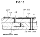
- a multi-chip module comprises a printed wiring board (100) and a plurality of bare IC chips (201 through 203), is mounted on a target printed wiring board (1), and is so arranged that: the printed wiring board has a multilayer structure; and within the multilayer structure, there are provided at least one dielectric layer both the sides of which are electrically connected to inner conductor layers within the multilayer structure.
- a multi-chip module according to a seventeenth aspect of the invention is so arranged that the dam frame is provided with a reinforcing part railing between two of the bare IC chips.
- a multi-chip module is so arranged that a dam frame is formed of a metal member in such a shape that the top of the dam frame is extend to cover the bare IC chips, and the bare IC chips are sealed with heat conductive resin so as to facilitate heat radiation from the bare IC chips.
- the multi-chip module is disposed on a flexible wiring board, which enables the three-dimensional disposition of multi-chip modules.
Landscapes
- Engineering & Computer Science (AREA)
- Microelectronics & Electronic Packaging (AREA)
- Structures For Mounting Electric Components On Printed Circuit Boards (AREA)
- Production Of Multi-Layered Print Wiring Board (AREA)
- Combinations Of Printed Boards (AREA)
Applications Claiming Priority (5)
| Application Number | Priority Date | Filing Date | Title |
|---|---|---|---|
| JP22864493 | 1993-09-14 | ||
| JP228644/93 | 1993-09-14 | ||
| JP19145594A JP3461204B2 (ja) | 1993-09-14 | 1994-08-15 | マルチチップモジュール |
| JP191455/94 | 1994-08-15 | ||
| PCT/JP1994/001517 WO1995008189A1 (fr) | 1993-09-14 | 1994-09-14 | Circuit multipuce |
Publications (3)
| Publication Number | Publication Date |
|---|---|
| EP0720232A1 true EP0720232A1 (fr) | 1996-07-03 |
| EP0720232A4 EP0720232A4 (fr) | 1996-11-13 |
| EP0720232B1 EP0720232B1 (fr) | 2007-04-11 |
Family
ID=26506700
Family Applications (1)
| Application Number | Title | Priority Date | Filing Date |
|---|---|---|---|
| EP94927045A Expired - Lifetime EP0720232B1 (fr) | 1993-09-14 | 1994-09-14 | Circuit multipuce |
Country Status (9)
| Country | Link |
|---|---|
| US (2) | US6147876A (fr) |
| EP (1) | EP0720232B1 (fr) |
| JP (1) | JP3461204B2 (fr) |
| CN (6) | CN1041035C (fr) |
| AU (1) | AU690920B2 (fr) |
| CA (1) | CA2171458C (fr) |
| DE (1) | DE69434952D1 (fr) |
| FI (1) | FI961176L (fr) |
| WO (1) | WO1995008189A1 (fr) |
Cited By (6)
| Publication number | Priority date | Publication date | Assignee | Title |
|---|---|---|---|---|
| WO1998007193A1 (fr) * | 1996-08-09 | 1998-02-19 | Robert Bosch Gmbh | Module multipuce |
| FR2852190A1 (fr) * | 2003-03-03 | 2004-09-10 | Wavecom | Procede de fabrication d'un composant ou d'un module electronique et composant ou module correspondant |
| EP0997935A4 (fr) * | 1997-04-11 | 2005-03-02 | Ibiden Co Ltd | Carte imprimee et son procede de fabrication |
| EP2624668A1 (fr) * | 2012-01-17 | 2013-08-07 | Huawei Device Co., Ltd. | Module intégré, tableau de système intégré et dispositif électronique |
| CN105555039A (zh) * | 2016-02-03 | 2016-05-04 | 江门崇达电路技术有限公司 | 一种在pcb的两焊盘间制作线条的方法 |
| US9831144B2 (en) | 2013-08-28 | 2017-11-28 | Qubeicon Ltd. | Semiconductor die and package jigsaw submount |
Families Citing this family (128)
| Publication number | Priority date | Publication date | Assignee | Title |
|---|---|---|---|---|
| DE19914305B4 (de) * | 1998-03-31 | 2004-11-25 | Kanji Higashiyamato Otsuka | Elektronische Vorrichtung |
| JP2000138423A (ja) * | 1998-10-30 | 2000-05-16 | Matsushita Electric Ind Co Ltd | プリント回路基板およびその製造方法 |
| WO2000033249A1 (fr) * | 1998-11-30 | 2000-06-08 | Hitachi, Ltd. | Procede de montage d'une puce de circuit electronique |
| US7382142B2 (en) | 2000-05-23 | 2008-06-03 | Nanonexus, Inc. | High density interconnect system having rapid fabrication cycle |
| US7247035B2 (en) | 2000-06-20 | 2007-07-24 | Nanonexus, Inc. | Enhanced stress metal spring contactor |
| US7349223B2 (en) * | 2000-05-23 | 2008-03-25 | Nanonexus, Inc. | Enhanced compliant probe card systems having improved planarity |
| US6812718B1 (en) | 1999-05-27 | 2004-11-02 | Nanonexus, Inc. | Massively parallel interface for electronic circuits |
| US6917525B2 (en) * | 2001-11-27 | 2005-07-12 | Nanonexus, Inc. | Construction structures and manufacturing processes for probe card assemblies and packages having wafer level springs |
| US6542379B1 (en) * | 1999-07-15 | 2003-04-01 | International Business Machines Corporation | Circuitry with integrated passive components and method for producing |
| JP2001160663A (ja) * | 1999-12-02 | 2001-06-12 | Nec Corp | 回路基板 |
| US6535398B1 (en) * | 2000-03-07 | 2003-03-18 | Fujitsu Limited | Multichip module substrates with buried discrete capacitors and components and methods for making |
| US6838766B2 (en) | 2000-03-21 | 2005-01-04 | Sanyo Electric Co., Ltd. | Semiconductor device |
| US7952373B2 (en) | 2000-05-23 | 2011-05-31 | Verigy (Singapore) Pte. Ltd. | Construction structures and manufacturing processes for integrated circuit wafer probe card assemblies |
| US7579848B2 (en) | 2000-05-23 | 2009-08-25 | Nanonexus, Inc. | High density interconnect system for IC packages and interconnect assemblies |
| TW502492B (en) * | 2000-05-30 | 2002-09-11 | Alps Electric Co Ltd | Electronic circuit unit |
| US6507100B1 (en) * | 2000-06-28 | 2003-01-14 | Advanced Micro Devices, Inc. | Cu-balanced substrate |
| US8629005B1 (en) | 2000-11-28 | 2014-01-14 | Knowles Electronics, Llc | Methods of manufacture of bottom port surface mount silicon condenser microphone packages |
| US7434305B2 (en) | 2000-11-28 | 2008-10-14 | Knowles Electronics, Llc. | Method of manufacturing a microphone |
| JP2002170739A (ja) * | 2000-11-29 | 2002-06-14 | Murata Mfg Co Ltd | 積層セラミックコンデンサモジュール |
| US6798666B1 (en) * | 2000-12-29 | 2004-09-28 | Ncr Corporation | Introducing loss in a power bus to reduce EMI and electrical noise |
| WO2002069680A2 (fr) * | 2001-01-17 | 2002-09-06 | Honeywell International Inc. | Adaptateur pour supports plastiques pour puce montee en surface (plcc) et autres supports de puce montes en surface (smt) |
| US6931369B1 (en) | 2001-05-01 | 2005-08-16 | National Semiconductor Corporation | Method to perform thermal simulation of an electronic circuit on a network |
| JP3675364B2 (ja) * | 2001-05-30 | 2005-07-27 | ソニー株式会社 | 半導体装置用基板その製造方法および半導体装置 |
| US6724083B2 (en) * | 2001-07-16 | 2004-04-20 | Ars Electronics Co., Ltd. | Method of producing semiconductor packages by cutting via holes into half when separating substrate |
| US6580613B2 (en) * | 2001-07-17 | 2003-06-17 | Infineon Technologies Ag | Solder-free PCB assembly |
| US6678877B1 (en) * | 2001-08-15 | 2004-01-13 | National Semiconductor Corporation | Creating a PC board (PCB) layout for a circuit in which the components of the circuit are placed in the determined PCB landing areas |
| US20030057544A1 (en) * | 2001-09-13 | 2003-03-27 | Nathan Richard J. | Integrated assembly protocol |
| US20030059976A1 (en) * | 2001-09-24 | 2003-03-27 | Nathan Richard J. | Integrated package and methods for making same |
| US6900991B2 (en) * | 2001-12-03 | 2005-05-31 | Intel Corporation | Electronic assembly with sandwiched capacitors and methods of manufacture |
| US20030153119A1 (en) * | 2002-02-14 | 2003-08-14 | Nathan Richard J. | Integrated circuit package and method for fabrication |
| US6639302B2 (en) * | 2002-03-20 | 2003-10-28 | International Business Machines Corporation | Stress reduction in flip-chip PBGA packaging by utilizing segmented chip carries |
| US6903458B1 (en) * | 2002-06-20 | 2005-06-07 | Richard J. Nathan | Embedded carrier for an integrated circuit chip |
| US20060213685A1 (en) * | 2002-06-27 | 2006-09-28 | Wang Alan E | Single or multi-layer printed circuit board with improved edge via design |
| US7005584B2 (en) * | 2004-02-13 | 2006-02-28 | Honeywell International Inc. | Compact navigation device assembly |
| KR101022539B1 (ko) * | 2004-04-29 | 2011-03-16 | 엘지디스플레이 주식회사 | 인쇄회로기판 및 액정표시장치 |
| JP2006100489A (ja) * | 2004-09-29 | 2006-04-13 | Ricoh Co Ltd | プリント基板及びそのプリント基板を用いた電子ユニット並びに樹脂流出防止用ダムの形成方法 |
| CN100395889C (zh) * | 2004-12-23 | 2008-06-18 | 旺宏电子股份有限公司 | 多芯片封装结构 |
| US7212395B2 (en) * | 2004-12-28 | 2007-05-01 | Intel Corporation | Capacitor design for controlling equivalent series resistance |
| JP4403090B2 (ja) * | 2005-03-02 | 2010-01-20 | 日東電工株式会社 | 配線回路基板 |
| JP4071782B2 (ja) * | 2005-05-30 | 2008-04-02 | 松下電器産業株式会社 | 半導体装置 |
| US7327006B2 (en) * | 2005-06-23 | 2008-02-05 | Nokia Corporation | Semiconductor package |
| JP4640802B2 (ja) * | 2005-07-07 | 2011-03-02 | 日東電工株式会社 | 回路付サスペンション基板 |
| JP4615427B2 (ja) * | 2005-12-01 | 2011-01-19 | 日東電工株式会社 | 配線回路基板 |
| US7589395B2 (en) * | 2006-06-30 | 2009-09-15 | Intel Corporation | Multiple-dice packages using elements between dice to control application of underfill material to reduce void formation |
| JP2008034639A (ja) * | 2006-07-28 | 2008-02-14 | Nitto Denko Corp | 配線回路基板 |
| JP4865453B2 (ja) * | 2006-08-30 | 2012-02-01 | 日東電工株式会社 | 配線回路基板およびその製造方法 |
| JP2008177491A (ja) * | 2007-01-22 | 2008-07-31 | Renesas Technology Corp | 半導体装置 |
| US7926173B2 (en) * | 2007-07-05 | 2011-04-19 | Occam Portfolio Llc | Method of making a circuit assembly |
| JP2008282995A (ja) * | 2007-05-10 | 2008-11-20 | Nitto Denko Corp | 配線回路基板 |
| US7829977B2 (en) * | 2007-11-15 | 2010-11-09 | Advanced Semiconductor Engineering, Inc. | Low temperature co-fired ceramics substrate and semiconductor package |
| USD602885S1 (en) * | 2008-04-04 | 2009-10-27 | Capres A/S | Connector for a microchip probe |
| AU323139S (en) * | 2008-05-15 | 2008-12-11 | Tyco Electronics Services Gmbh | Printed circuit board |
| AU2009248414B2 (en) * | 2008-05-15 | 2014-05-29 | Tyco Electronics Services Gmbh | Circuit board for electrical connector and electrical connector |
| CN101394708B (zh) * | 2008-10-20 | 2012-11-28 | 李鑫 | 一种电路板及其设计方法 |
| JP4740312B2 (ja) * | 2008-12-18 | 2011-08-03 | 日東電工株式会社 | 配線回路基板集合体シート |
| USD794642S1 (en) * | 2009-01-07 | 2017-08-15 | Samsung Electronics Co., Ltd. | Memory device |
| USD795261S1 (en) * | 2009-01-07 | 2017-08-22 | Samsung Electronics Co., Ltd. | Memory device |
| USD794034S1 (en) * | 2009-01-07 | 2017-08-08 | Samsung Electronics Co., Ltd. | Memory device |
| USD794641S1 (en) * | 2009-01-07 | 2017-08-15 | Samsung Electronics Co., Ltd. | Memory device |
| USD794643S1 (en) * | 2009-01-07 | 2017-08-15 | Samsung Electronics Co., Ltd. | Memory device |
| USD795262S1 (en) * | 2009-01-07 | 2017-08-22 | Samsung Electronics Co., Ltd. | Memory device |
| USD794644S1 (en) * | 2009-01-07 | 2017-08-15 | Samsung Electronics Co., Ltd. | Memory device |
| US8071893B2 (en) | 2009-03-04 | 2011-12-06 | Apple Inc. | Methods and apparatus for shielding circuitry from interference |
| USD639812S1 (en) * | 2010-05-17 | 2011-06-14 | Panasonic Corporation | Memory card |
| USD643040S1 (en) * | 2010-10-26 | 2011-08-09 | Hon Hai Precision Ind. Co., Ltd. | Electrical card |
| KR101458481B1 (ko) * | 2010-11-02 | 2014-11-07 | 쿄세라 코포레이션 | 멀티파트 배선 기판, 배선 기판, 및 전자 장치 |
| US9374643B2 (en) | 2011-11-04 | 2016-06-21 | Knowles Electronics, Llc | Embedded dielectric as a barrier in an acoustic device and method of manufacture |
| USD680545S1 (en) * | 2011-11-15 | 2013-04-23 | Connectblue Ab | Module |
| USD668659S1 (en) * | 2011-11-15 | 2012-10-09 | Connectblue Ab | Module |
| USD692896S1 (en) * | 2011-11-15 | 2013-11-05 | Connectblue Ab | Module |
| USD668658S1 (en) * | 2011-11-15 | 2012-10-09 | Connectblue Ab | Module |
| USD680119S1 (en) * | 2011-11-15 | 2013-04-16 | Connectblue Ab | Module |
| USD689053S1 (en) * | 2011-11-15 | 2013-09-03 | Connectblue Ab | Module |
| KR101964045B1 (ko) * | 2012-04-12 | 2019-04-01 | 삼성전자주식회사 | 반도체 메모리 모듈 및 그 제조 방법 |
| US9078063B2 (en) | 2012-08-10 | 2015-07-07 | Knowles Electronics, Llc | Microphone assembly with barrier to prevent contaminant infiltration |
| USD709894S1 (en) * | 2012-09-22 | 2014-07-29 | Apple Inc. | Electronic device |
| DE202013011995U1 (de) * | 2013-01-22 | 2015-01-15 | Baumüller Nürnberg GmbH | Leiterplattenanordnung |
| JP6202721B2 (ja) * | 2013-04-08 | 2017-09-27 | アオイ電子株式会社 | 回路基板およびそれを用いたサーマルプリントヘッド |
| CN104102387A (zh) * | 2014-08-01 | 2014-10-15 | 金龙机电(东莞)有限公司 | 一种触摸屏和触摸屏装置 |
| US9936580B1 (en) * | 2015-01-14 | 2018-04-03 | Vlt, Inc. | Method of forming an electrical connection to an electronic module |
| US9967984B1 (en) * | 2015-01-14 | 2018-05-08 | Vlt, Inc. | Power adapter packaging |
| US10264664B1 (en) | 2015-06-04 | 2019-04-16 | Vlt, Inc. | Method of electrically interconnecting circuit assemblies |
| US10165690B2 (en) * | 2015-06-19 | 2018-12-25 | Nippon Telegraph And Telephone Corporation | Solder joint structure of flexible printed circuit board |
| US9794661B2 (en) | 2015-08-07 | 2017-10-17 | Knowles Electronics, Llc | Ingress protection for reducing particle infiltration into acoustic chamber of a MEMS microphone package |
| KR20170046344A (ko) * | 2015-10-21 | 2017-05-02 | 삼성전자주식회사 | 반도체 장치 및 이를 포함하는 반도체 패키지 |
| US10158357B1 (en) | 2016-04-05 | 2018-12-18 | Vlt, Inc. | Method and apparatus for delivering power to semiconductors |
| US10903734B1 (en) | 2016-04-05 | 2021-01-26 | Vicor Corporation | Delivering power to semiconductor loads |
| JP6677183B2 (ja) * | 2017-01-25 | 2020-04-08 | オムロン株式会社 | 制御装置 |
| USD826194S1 (en) * | 2017-05-26 | 2018-08-21 | TinyPCB, Inc. | Modular circuit board |
| USD826191S1 (en) * | 2017-05-26 | 2018-08-21 | TinyPCB, Inc. | Modular circuit board |
| USD829675S1 (en) * | 2017-05-26 | 2018-10-02 | TinyPCB, Inc. | Modular circuit board |
| USD824345S1 (en) * | 2017-05-26 | 2018-07-31 | TinyPCB, Inc. | Modular circuit board |
| USD826193S1 (en) * | 2017-05-26 | 2018-08-21 | TinyPCB, Inc. | Modular circuit board |
| USD829674S1 (en) * | 2017-05-26 | 2018-10-02 | TinyPCB, Inc. | Modular circuit board |
| USD826186S1 (en) * | 2017-05-26 | 2018-08-21 | TinyPCB, Inc. | Modular circuit board |
| USD824344S1 (en) * | 2017-05-26 | 2018-07-31 | TinyPCB, Inc. | Modular circuit board |
| USD826188S1 (en) * | 2017-05-26 | 2018-08-21 | TinyPCB, Inc. | Modular circuit board |
| USD826195S1 (en) * | 2017-05-26 | 2018-08-21 | TinyPCB, Inc. | Modular circuit board |
| USD826196S1 (en) * | 2017-05-26 | 2018-08-21 | TinyPCB, Inc. | Modular circuit board |
| USD826187S1 (en) * | 2017-05-26 | 2018-08-21 | TinyPCB, Inc. | Modular circuit board |
| USD826189S1 (en) * | 2017-05-26 | 2018-08-21 | TinyPCB, Inc. | Modular circuit board |
| USD832229S1 (en) * | 2017-05-26 | 2018-10-30 | TinyPCB, Inc. | Modular circuit board |
| USD826190S1 (en) * | 2017-05-26 | 2018-08-21 | TinyPCB, Inc. | Modular circuit board |
| USD830318S1 (en) * | 2017-05-26 | 2018-10-09 | TinyPCB, Inc. | Moduler circuit board |
| USD826192S1 (en) * | 2017-05-26 | 2018-08-21 | TinyPCB, Inc. | Modular circuit board |
| USD833991S1 (en) * | 2017-05-30 | 2018-11-20 | TinyPCB, Inc. | Modular circuit board |
| USD833993S1 (en) * | 2017-05-30 | 2018-11-20 | TinyPCB, Inc. | Modular circuit board |
| USD833994S1 (en) * | 2017-05-30 | 2018-11-20 | TinyPCB, Inc. | Modular circuit board |
| USD834546S1 (en) * | 2017-05-30 | 2018-11-27 | TinyPCB, Inc. | Modular circuit board |
| USD839222S1 (en) * | 2017-05-30 | 2019-01-29 | TinyPCB, Inc. | Modular circuit board |
| USD833990S1 (en) * | 2017-05-30 | 2018-11-20 | TinyPCB, Inc. | Modular circuit board |
| USD839223S1 (en) * | 2017-05-30 | 2019-01-29 | TinyPCB, Inc. | Modular circuit board |
| USD841606S1 (en) * | 2017-05-30 | 2019-02-26 | TinyPCB, Inc. | Modular circuit board |
| USD833992S1 (en) * | 2017-05-30 | 2018-11-20 | TinyPCB, Inc. | Modular circuit board |
| USD830320S1 (en) * | 2017-05-30 | 2018-10-09 | TinyPCB, Inc. | Modular circuit board |
| USD841605S1 (en) * | 2017-05-30 | 2019-02-26 | TinyPCB, Inc. | Modular circuit board |
| USD830321S1 (en) * | 2017-05-30 | 2018-10-09 | TinyPCB, Inc. | Modular circuit board |
| USD842260S1 (en) * | 2017-05-30 | 2019-03-05 | TinyPCB, Inc. | Modular circuit board |
| USD830319S1 (en) * | 2017-05-30 | 2018-10-09 | TinyPCB, Inc. | Modular circuit board |
| USD839221S1 (en) * | 2017-05-30 | 2019-01-29 | TinyPCB, Inc. | Modular circuit board |
| TWI647581B (zh) * | 2017-11-22 | 2019-01-11 | 緯創資通股份有限公司 | 電路板以及佈局結構 |
| CN110139477B (zh) * | 2018-02-09 | 2021-10-08 | 台达电子企业管理(上海)有限公司 | 应用于智能终端的电源模块及电源模块组装结构 |
| WO2020061330A1 (fr) * | 2018-09-19 | 2020-03-26 | Tesla, Inc. | Architecture mécanique pour module multi-puce |
| US11107753B2 (en) * | 2018-11-28 | 2021-08-31 | Semiconductor Components Industries, Llc | Packaging structure for gallium nitride devices |
| US11201602B1 (en) | 2020-09-17 | 2021-12-14 | Analog Devices, Inc. | Apparatus and methods for tunable filtering |
| US11201600B1 (en) | 2020-10-05 | 2021-12-14 | Analog Devices, Inc. | Apparatus and methods for control and calibration of tunable filters |
| DE102021113302A1 (de) * | 2021-05-21 | 2022-11-24 | Infineon Technologies Ag | Board mit Zinnen |
| CN114188235B (zh) * | 2022-02-15 | 2022-04-19 | 江苏高格芯微电子有限公司 | 一种低功耗高精度协议集成电路模组封装工艺 |
Family Cites Families (59)
| Publication number | Priority date | Publication date | Assignee | Title |
|---|---|---|---|---|
| FR1452108A (fr) * | 1964-07-29 | 1966-02-25 | Telefunken Patent | Procédé de fabrication d'un montage microminiaturisé |
| US3714709A (en) * | 1970-07-06 | 1973-02-06 | Rca Corp | Method of manufacturing thick-film hybrid integrated circuits |
| US3689804A (en) * | 1971-09-30 | 1972-09-05 | Nippon Denso Co | Hybrid circuit device |
| US3885304A (en) * | 1972-03-23 | 1975-05-27 | Bosch Gmbh Robert | Electric circuit arrangement and method of making the same |
| US4372037A (en) * | 1975-03-03 | 1983-02-08 | Hughes Aircraft Company | Large area hybrid microcircuit assembly |
| US4208698A (en) * | 1977-10-26 | 1980-06-17 | Ilc Data Device Corporation | Novel hybrid packaging scheme for high density component circuits |
| JPS5687395A (en) * | 1979-12-18 | 1981-07-15 | Fujitsu Ltd | Semiconductor device |
| US4349862A (en) * | 1980-08-11 | 1982-09-14 | International Business Machines Corporation | Capacitive chip carrier and multilayer ceramic capacitors |
| US4437141A (en) * | 1981-09-14 | 1984-03-13 | Texas Instruments Incorporated | High terminal count integrated circuit device package |
| DE3382208D1 (de) * | 1982-12-15 | 1991-04-18 | Nec Corp | Monolithisches vielschichtkeramiksubstrat mit mindestens einer dielektrischen schicht aus einem material mit perovskit-struktur. |
| GB2144907A (en) * | 1983-08-09 | 1985-03-13 | Standard Telephones Cables Ltd | Mounting integrated circuit devices |
| CA1222586A (fr) * | 1983-11-11 | 1987-06-02 | Tadahiko Akiyama | Systeme de communication offrant des services personnels |
| US4616655A (en) * | 1984-01-20 | 1986-10-14 | Cordis Corporation | Implantable pulse generator having a single printed circuit board and a chip carrier |
| JPS60173862A (ja) * | 1984-02-20 | 1985-09-07 | Nec Corp | 集積回路装置 |
| US5237204A (en) * | 1984-05-25 | 1993-08-17 | Compagnie D'informatique Militaire Spatiale Et Aeronautique | Electric potential distribution device and an electronic component case incorporating such a device |
| US4692839A (en) * | 1985-06-24 | 1987-09-08 | Digital Equipment Corporation | Multiple chip interconnection system and package |
| US5220488A (en) * | 1985-09-04 | 1993-06-15 | Ufe Incorporated | Injection molded printed circuits |
| US4780795A (en) * | 1986-04-28 | 1988-10-25 | Burr-Brown Corporation | Packages for hybrid integrated circuit high voltage isolation amplifiers and method of manufacture |
| JPS62260353A (ja) * | 1986-05-06 | 1987-11-12 | Mitsubishi Electric Corp | 半導体装置 |
| JPS62260354A (ja) * | 1986-05-06 | 1987-11-12 | Mitsubishi Electric Corp | 半導体装置 |
| US4814943A (en) * | 1986-06-04 | 1989-03-21 | Oki Electric Industry Co., Ltd. | Printed circuit devices using thermoplastic resin cover plate |
| WO1988002183A1 (fr) * | 1986-09-19 | 1988-03-24 | Hughes Aircraft Company | Ebarbage de composants passifs noyes dans des structures multicouches |
| JPS63104361A (ja) * | 1986-10-20 | 1988-05-09 | Mitsubishi Electric Corp | 半導体装置 |
| US4811082A (en) * | 1986-11-12 | 1989-03-07 | International Business Machines Corporation | High performance integrated circuit packaging structure |
| GB2197540B (en) * | 1986-11-12 | 1991-04-17 | Murata Manufacturing Co | A circuit structure. |
| FI82169C (fi) * | 1987-08-21 | 1991-01-10 | Nokia Mobira Oy | Rf-skyddad hybridkrets. |
| US4788524A (en) * | 1987-08-27 | 1988-11-29 | Gte Communication Systems Corporation | Thick film material system |
| WO1989004552A1 (fr) * | 1987-10-30 | 1989-05-18 | Lsi Logic Corporation | Procede et agencement de fabrication de boitiers de dispositifs semi-conducteurs |
| US4882657A (en) * | 1988-04-06 | 1989-11-21 | Ici Array Technology, Inc. | Pin grid array assembly |
| EP0339154B1 (fr) * | 1988-04-26 | 1994-11-17 | Citizen Watch Co. Ltd. | carte mémoire |
| US5253010A (en) * | 1988-05-13 | 1993-10-12 | Minolta Camera Kabushiki Kaisha | Printed circuit board |
| JP2570381B2 (ja) * | 1988-05-13 | 1997-01-08 | ミノルタ株式会社 | フレキシブルプリント基板へのicチツプ搭載構造 |
| EP0351581A1 (fr) * | 1988-07-22 | 1990-01-24 | Oerlikon-Contraves AG | Circuit intégré à haute densité et procédé pour sa fabrication |
| JPH02106087A (ja) * | 1988-10-14 | 1990-04-18 | Rohm Co Ltd | 混成集積回路装置 |
| KR930010076B1 (ko) * | 1989-01-14 | 1993-10-14 | 티디케이 가부시키가이샤 | 다층혼성집적회로 |
| JP2790640B2 (ja) * | 1989-01-14 | 1998-08-27 | ティーディーケイ株式会社 | 混成集積回路部品の構造 |
| JP3090453B2 (ja) * | 1989-07-10 | 2000-09-18 | 株式会社日立製作所 | 厚膜薄膜積層基板およびそれを用いた電子回路装置 |
| US5200362A (en) * | 1989-09-06 | 1993-04-06 | Motorola, Inc. | Method of attaching conductive traces to an encapsulated semiconductor die using a removable transfer film |
| US5045820A (en) * | 1989-09-27 | 1991-09-03 | Motorola, Inc. | Three-dimensional microwave circuit carrier and integral waveguide coupler |
| MY105486A (en) * | 1989-12-15 | 1994-10-31 | Tdk Corp | A multilayer hybrid circuit. |
| NO900229D0 (no) * | 1990-01-16 | 1990-01-16 | Micro Electronics Ame A S | Fremgangsmaate for fremstilling av miniatyrisert impedanstilpasset ledningsnett. |
| JPH04130470A (ja) * | 1990-09-21 | 1992-05-01 | Mita Ind Co Ltd | 画像形成装置のための自己診断および自己修復システム |
| US5557142A (en) * | 1991-02-04 | 1996-09-17 | Motorola, Inc. | Shielded semiconductor device package |
| US5166772A (en) * | 1991-02-22 | 1992-11-24 | Motorola, Inc. | Transfer molded semiconductor device package with integral shield |
| FR2675632B1 (fr) * | 1991-04-18 | 1997-04-30 | Texas Instruments France | Dispositif de conditionnement de circuits integres |
| JPH04335561A (ja) * | 1991-05-13 | 1992-11-24 | Mitsubishi Electric Corp | 半導体装置 |
| JPH04130470U (ja) * | 1991-05-21 | 1992-11-30 | シヤープ株式会社 | 半導体装置 |
| EP0585376A4 (en) * | 1991-05-23 | 1994-06-08 | Motorola Inc | Integrated circuit chip carrier |
| JP2976605B2 (ja) * | 1991-08-26 | 1999-11-10 | ソニー株式会社 | メモリモジュール |
| JPH05102262A (ja) * | 1991-10-03 | 1993-04-23 | Hitachi Ltd | 半導体装置及びそれを実装した実装装置 |
| JPH05206314A (ja) * | 1991-11-12 | 1993-08-13 | Nec Corp | 半導体装置 |
| JPH05160290A (ja) * | 1991-12-06 | 1993-06-25 | Rohm Co Ltd | 回路モジュール |
| US5854534A (en) * | 1992-08-05 | 1998-12-29 | Fujitsu Limited | Controlled impedence interposer substrate |
| JPH0798620A (ja) * | 1992-11-13 | 1995-04-11 | Seiko Epson Corp | 電子装置およびこれを用いたコンピュータ |
| US5241351A (en) * | 1992-11-19 | 1993-08-31 | Xerox Corporation | Multi-blade turret holder |
| JPH06267788A (ja) * | 1993-03-15 | 1994-09-22 | Murata Mfg Co Ltd | 複合部品 |
| US5355016A (en) * | 1993-05-03 | 1994-10-11 | Motorola, Inc. | Shielded EPROM package |
| GB2283863A (en) * | 1993-11-16 | 1995-05-17 | Ibm | Direct chip attach module |
| WO1996019829A1 (fr) * | 1994-12-22 | 1996-06-27 | Pace Benedict G | Dispositif de surchauffe de la vapeur |
-
1994
- 1994-08-15 JP JP19145594A patent/JP3461204B2/ja not_active Expired - Fee Related
- 1994-09-14 WO PCT/JP1994/001517 patent/WO1995008189A1/fr not_active Ceased
- 1994-09-14 CN CN94193352A patent/CN1041035C/zh not_active Expired - Fee Related
- 1994-09-14 US US08/617,843 patent/US6147876A/en not_active Expired - Fee Related
- 1994-09-14 EP EP94927045A patent/EP0720232B1/fr not_active Expired - Lifetime
- 1994-09-14 DE DE69434952T patent/DE69434952D1/de not_active Expired - Lifetime
- 1994-09-14 CA CA002171458A patent/CA2171458C/fr not_active Expired - Fee Related
- 1994-09-14 AU AU76650/94A patent/AU690920B2/en not_active Ceased
- 1994-09-14 FI FI961176A patent/FI961176L/fi unknown
-
1998
- 1998-04-27 CN CN98107886A patent/CN1214547A/zh active Pending
- 1998-04-27 CN CN98107887A patent/CN1198593A/zh active Pending
- 1998-04-27 CN CN98107888A patent/CN1214548A/zh active Pending
- 1998-04-27 CN CN98107889A patent/CN1198594A/zh active Pending
- 1998-04-27 CN CN98107885A patent/CN1203454A/zh active Pending
-
2000
- 2000-08-11 US US09/636,714 patent/US6418030B1/en not_active Expired - Fee Related
Cited By (8)
| Publication number | Priority date | Publication date | Assignee | Title |
|---|---|---|---|---|
| WO1998007193A1 (fr) * | 1996-08-09 | 1998-02-19 | Robert Bosch Gmbh | Module multipuce |
| US5953213A (en) * | 1996-08-09 | 1999-09-14 | Robert Bosch Gmbh | Multichip module |
| EP0997935A4 (fr) * | 1997-04-11 | 2005-03-02 | Ibiden Co Ltd | Carte imprimee et son procede de fabrication |
| FR2852190A1 (fr) * | 2003-03-03 | 2004-09-10 | Wavecom | Procede de fabrication d'un composant ou d'un module electronique et composant ou module correspondant |
| EP2624668A1 (fr) * | 2012-01-17 | 2013-08-07 | Huawei Device Co., Ltd. | Module intégré, tableau de système intégré et dispositif électronique |
| US9831144B2 (en) | 2013-08-28 | 2017-11-28 | Qubeicon Ltd. | Semiconductor die and package jigsaw submount |
| CN105555039A (zh) * | 2016-02-03 | 2016-05-04 | 江门崇达电路技术有限公司 | 一种在pcb的两焊盘间制作线条的方法 |
| CN105555039B (zh) * | 2016-02-03 | 2018-10-02 | 江门崇达电路技术有限公司 | 一种在pcb的两焊盘间制作线条的方法 |
Also Published As
| Publication number | Publication date |
|---|---|
| JP3461204B2 (ja) | 2003-10-27 |
| WO1995008189A1 (fr) | 1995-03-23 |
| US6147876A (en) | 2000-11-14 |
| FI961176A0 (fi) | 1996-03-13 |
| CN1198593A (zh) | 1998-11-11 |
| CA2171458A1 (fr) | 1995-03-23 |
| CN1041035C (zh) | 1998-12-02 |
| AU690920B2 (en) | 1998-05-07 |
| EP0720232A4 (fr) | 1996-11-13 |
| US6418030B1 (en) | 2002-07-09 |
| CN1198594A (zh) | 1998-11-11 |
| CN1130958A (zh) | 1996-09-11 |
| EP0720232B1 (fr) | 2007-04-11 |
| DE69434952D1 (de) | 2007-05-24 |
| AU7665094A (en) | 1995-04-03 |
| JPH07135290A (ja) | 1995-05-23 |
| CN1214547A (zh) | 1999-04-21 |
| CA2171458C (fr) | 2001-11-27 |
| FI961176A7 (fi) | 1996-03-13 |
| FI961176L (fi) | 1996-03-13 |
| CN1203454A (zh) | 1998-12-30 |
| CN1214548A (zh) | 1999-04-21 |
Similar Documents
| Publication | Publication Date | Title |
|---|---|---|
| US6147876A (en) | Multi-chip module having printed wiring board comprising circuit pattern for IC chip | |
| KR100231276B1 (ko) | 반도체패키지의 구조 및 제조방법 | |
| US5953589A (en) | Ball grid array semiconductor package with solder balls fused on printed circuit board and method for fabricating the same | |
| US7639513B2 (en) | Radio frequency module and manufacturing method thereof | |
| US7613010B2 (en) | Stereoscopic electronic circuit device, and relay board and relay frame used therein | |
| US5854512A (en) | High density leaded ball-grid array package | |
| US6072233A (en) | Stackable ball grid array package | |
| KR100694739B1 (ko) | 다수의 전원/접지면을 갖는 볼 그리드 어레이 패키지 | |
| US10229888B2 (en) | Systems and methods for providing electromagnetic interference (EMI) compartment shielding for components disposed inside of system electronic packages | |
| US7236373B2 (en) | Electronic device capable of preventing electromagnetic wave from being radiated | |
| EP0377932A2 (fr) | Ensemble de circuits intégrés à semiconducteur | |
| JP2011040602A (ja) | 電子装置およびその製造方法 | |
| US7049687B2 (en) | Tape carrier package having stacked semiconductor elements, and short and long leads | |
| EP1647168A1 (fr) | Module multipuce surmoule dont les composants montes en surface presentent une fiabilite accrue | |
| KR100240748B1 (ko) | 기판을 갖는 반도체 칩 패키지와 그 제조 방법 및 그를 이용한적층 패키지 | |
| US10178757B2 (en) | Systems and methods for providing electromagnetic interference (EMI) compartment shielding for components disposed inside of system electronic packages | |
| US7320604B2 (en) | Electronic circuit module and method for fabrication thereof | |
| CN112992776A (zh) | 封装方法、封装结构及封装模块 | |
| US20010022391A1 (en) | Substrate for semiconductor device and semiconductor device fabrication using the same | |
| CN121215619A (zh) | 具有集成天线的半导体封装及其形成方法 | |
| CA2355615C (fr) | Module multipuce | |
| JPH0517709B2 (fr) | ||
| JPH11102991A (ja) | 半導体素子搭載フレーム | |
| KR20090049015A (ko) | 회로 모듈 | |
| KR100195511B1 (ko) | 리드 프레임을 이용한 볼 그리드 어레이 패키지 |
Legal Events
| Date | Code | Title | Description |
|---|---|---|---|
| PUAI | Public reference made under article 153(3) epc to a published international application that has entered the european phase |
Free format text: ORIGINAL CODE: 0009012 |
|
| 17P | Request for examination filed |
Effective date: 19960306 |
|
| AK | Designated contracting states |
Kind code of ref document: A1 Designated state(s): DE FR GB NL SE |
|
| A4 | Supplementary search report drawn up and despatched | ||
| AK | Designated contracting states |
Kind code of ref document: A4 Designated state(s): DE FR GB NL SE |
|
| 17Q | First examination report despatched |
Effective date: 20020514 |
|
| GRAP | Despatch of communication of intention to grant a patent |
Free format text: ORIGINAL CODE: EPIDOSNIGR1 |
|
| GRAS | Grant fee paid |
Free format text: ORIGINAL CODE: EPIDOSNIGR3 |
|
| GRAA | (expected) grant |
Free format text: ORIGINAL CODE: 0009210 |
|
| AK | Designated contracting states |
Kind code of ref document: B1 Designated state(s): DE FR GB NL SE |
|
| REG | Reference to a national code |
Ref country code: GB Ref legal event code: FG4D |
|
| REF | Corresponds to: |
Ref document number: 69434952 Country of ref document: DE Date of ref document: 20070524 Kind code of ref document: P |
|
| PG25 | Lapsed in a contracting state [announced via postgrant information from national office to epo] |
Ref country code: SE Free format text: LAPSE BECAUSE OF FAILURE TO SUBMIT A TRANSLATION OF THE DESCRIPTION OR TO PAY THE FEE WITHIN THE PRESCRIBED TIME-LIMIT Effective date: 20070711 |
|
| PGFP | Annual fee paid to national office [announced via postgrant information from national office to epo] |
Ref country code: DE Payment date: 20070906 Year of fee payment: 14 |
|
| NLV1 | Nl: lapsed or annulled due to failure to fulfill the requirements of art. 29p and 29m of the patents act | ||
| EN | Fr: translation not filed | ||
| PG25 | Lapsed in a contracting state [announced via postgrant information from national office to epo] |
Ref country code: NL Free format text: LAPSE BECAUSE OF FAILURE TO SUBMIT A TRANSLATION OF THE DESCRIPTION OR TO PAY THE FEE WITHIN THE PRESCRIBED TIME-LIMIT Effective date: 20070411 |
|
| PLBE | No opposition filed within time limit |
Free format text: ORIGINAL CODE: 0009261 |
|
| STAA | Information on the status of an ep patent application or granted ep patent |
Free format text: STATUS: NO OPPOSITION FILED WITHIN TIME LIMIT |
|
| 26N | No opposition filed |
Effective date: 20080114 |
|
| PG25 | Lapsed in a contracting state [announced via postgrant information from national office to epo] |
Ref country code: FR Free format text: LAPSE BECAUSE OF FAILURE TO SUBMIT A TRANSLATION OF THE DESCRIPTION OR TO PAY THE FEE WITHIN THE PRESCRIBED TIME-LIMIT Effective date: 20071207 Ref country code: DE Free format text: LAPSE BECAUSE OF FAILURE TO SUBMIT A TRANSLATION OF THE DESCRIPTION OR TO PAY THE FEE WITHIN THE PRESCRIBED TIME-LIMIT Effective date: 20070712 |
|
| PGFP | Annual fee paid to national office [announced via postgrant information from national office to epo] |
Ref country code: FR Payment date: 20070914 Year of fee payment: 14 |
|
| REG | Reference to a national code |
Ref country code: GB Ref legal event code: 746 Effective date: 20090517 |
|
| PGFP | Annual fee paid to national office [announced via postgrant information from national office to epo] |
Ref country code: GB Payment date: 20110914 Year of fee payment: 18 |
|
| GBPC | Gb: european patent ceased through non-payment of renewal fee |
Effective date: 20120914 |
|
| PG25 | Lapsed in a contracting state [announced via postgrant information from national office to epo] |
Ref country code: GB Free format text: LAPSE BECAUSE OF NON-PAYMENT OF DUE FEES Effective date: 20120914 |