EP0720320B1 - Circuit de traitement d'un signal transmis pouvant déterminer la valeur optimale du seuil de justification selon le genre d'unité tributaire du signal d'entrée - Google Patents
Circuit de traitement d'un signal transmis pouvant déterminer la valeur optimale du seuil de justification selon le genre d'unité tributaire du signal d'entrée Download PDFInfo
- Publication number
- EP0720320B1 EP0720320B1 EP95120568A EP95120568A EP0720320B1 EP 0720320 B1 EP0720320 B1 EP 0720320B1 EP 95120568 A EP95120568 A EP 95120568A EP 95120568 A EP95120568 A EP 95120568A EP 0720320 B1 EP0720320 B1 EP 0720320B1
- Authority
- EP
- European Patent Office
- Prior art keywords
- stuff
- signal
- input
- circuit
- threshold value
- Prior art date
- Legal status (The legal status is an assumption and is not a legal conclusion. Google has not performed a legal analysis and makes no representation as to the accuracy of the status listed.)
- Expired - Lifetime
Links
Images

Classifications
-
- H—ELECTRICITY
- H04—ELECTRIC COMMUNICATION TECHNIQUE
- H04J—MULTIPLEX COMMUNICATION
- H04J3/00—Time-division multiplex systems
- H04J3/02—Details
- H04J3/06—Synchronising arrangements
- H04J3/062—Synchronisation of signals having the same nominal but fluctuating bit rates, e.g. using buffers
- H04J3/0623—Synchronous multiplexing systems, e.g. synchronous digital hierarchy/synchronous optical network (SDH/SONET), synchronisation with a pointer process
-
- H—ELECTRICITY
- H04—ELECTRIC COMMUNICATION TECHNIQUE
- H04J—MULTIPLEX COMMUNICATION
- H04J3/00—Time-division multiplex systems
- H04J3/02—Details
- H04J3/06—Synchronising arrangements
- H04J3/07—Synchronising arrangements using pulse stuffing for systems with different or fluctuating information rates or bit rates
- H04J3/076—Bit and byte stuffing, e.g. SDH/PDH desynchronisers, bit-leaking
Definitions
- This invention relates to a synchronous digital multiplexing transmission device for dealing with an input transmission signal based on a synchronous digital hierarchy (SDH) and, more particularly, to a transmission signal processing circuit for use in the synchronous digital multiplexing transmission device in processing the input transmission signal into an output transmission signal.
- SDH synchronous digital hierarchy
- a transmission signal processing circuit of the type described is supplied from a transmission line with an input transmission signal which comprises an input frame (namely, a transmission line frame).
- the input frame (or the transmission line frame) comprises an input pointer and a datum which is typically a tributary unit (TU).
- the input pointer designates a location of a leading edge of the TU in the input frame.
- the transmission signal processing circuit processes the input transmission signal into an output transmission signal comprising an output frame (namely, a device frame).
- the output frame (or the device frame) comprises an output pointer and the TU.
- the output pointer designates another location of the leading edge of the TU in the output frame.
- the transmission signal processing circuit transfers the TU from the input frame onto the output frame.
- the transmission signal processing circuit is called a TU pointer processing circuit as known in the art.
- the TU is defined as a frame used in multiplexing digital signals.
- SDH synchronous digital hierarchy
- ITU-T Telecommunication Standardization Sector of International Telecommunication Union: previously CCITT
- the TU is defined as a frame used in multiplexing digital signals.
- the digital signals having a bit rate of 1.544 Mbits/s in common use is made of a TU-11 as the TU.
- the digital signals having another bit rate of 2.048 Mbits/s in common use is made of a TU-12 as the TU.
- a TU-2 For the digital signals having still another bit rate of 6.312 Mbits/s in common, use is made of a TU-2 as the TU.
- a TU-3 is used as the TU.
- the TU's of four sorts or types namely, the TU-11, the TU-12, the TU-2, and the TU-3 are present in correspondence to signal rates (or the bit rates) of the digital signals.
- a conventional transmission signal processing circuit includes a write controller which controls writing of the tributary unit of the input frame in a memory in response to a location signal representative of a location of the TU in the input frame by supplying a write address signal to the memory.
- a read controller controls reading of the tributary unit out of the memory in response to a stuff request signal by supplying a read address signal to the memory.
- a stuff execution judgement circuit is given an input stuff threshold value and judges whether or not a stuff operation should be executed by comparing a difference between the write address signal and the read address signal with the input stuff threshold value. The stuff execution judgement circuit produces the stuff request signal when the stuff execution judgement circuit judges that the stuff operation should be executed.
- the stuff execution judgement circuit is given the input stuff threshold value which is constant or fixed no matter whether the TU of the input frame has any signal rate.
- the input stuff threshold value is constant or fixed for the TU's of four sorts (namely, the TU-11, the TU-12, the TU-2, and the TU-3). This results in an increase of a delay required from a write timing of the TU in the memory to a read timing of the TU under consideration out of the memory when the TU under consideration has a particular signal rate selected from the bit rates of the TU's of four sorts. This is because optimum stuff threshold values are different from one another for the signal rates of the TU's of four sorts.
- a transmission signal processing circuit is disclosed in JP-A-02-81527 as explained below.
- TU tributary unit
- the transmission signal processing circuit is equivalent to the transmission signal processing circuit described in the preamble of this instant specification and is substantially equivalent to a TU (namely, a tributary unit) pointer processing circuit disclosed in JP-A- 02-81527.
- the transmission signal processing circuit is for use in a synchronous digital multiplexing transmission device (not shown) and is supplied from a transmission line (not shown) with an input transmission signal 10 synchronized with input clock pulses.
- the input transmission signal comprises an input frame (namely, a transmission line frame) which is synchronized with an input frame pulse and which includes a TU.
- the transmission signal processing circuit is further supplied with output clock pulses and an output frame pulse from the synchronous digital multiplexing transmission device.
- the transmission signal processing circuit processes the input transmission signal into an output transmission signal 11 comprising an output frame (namely, a device frame) including the tributary unit by transferring the tributary unit from the input frame onto the output frame of the output transmission signal 11 with the output transmission signal 11 synchronized with the output clock pulses and with the output frame synchronized with the output frame pulse.
- an output transmission signal 11 comprising an output frame (namely, a device frame) including the tributary unit by transferring the tributary unit from the input frame onto the output frame of the output transmission signal 11 with the output transmission signal 11 synchronized with the output clock pulses and with the output frame synchronized with the output frame pulse.
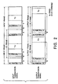
- the input transmission signal 10 of Fig. 1 is depicted along a first or top row.
- the input transmission signal includes an AU (administration unit) pointer which designates a location X of a leading edge of a VC (virtual container) frame in the input frame.
- the input transmission signal further includes a TU pointer in the input frame with a fixed interval N left between the leading edge of the VC frame and the TU pointer.
- the TU pointer designates another location Y of a leading edge of the TU in the input frame.
- An input pointer described in the preamble of the instant specification corresponds to the TU pointer which designates the location Y of the leading edge of the TU in the input frame.
- the output transmission signal 11 of Fig. 1 is depicted along a second or bottom row.
- the output transmission signal includes the AU pointer which designates the location 0 (zero) of the leading edge of the VC frame in the output frame.
- the output transmission signal further includes the TU pointer in the output frame with the fixed interval N left between the leading edge of the VC frame and the TU pointer.
- the TU pointer designates still another location Z of the leading edge of the TU in the output frame.
- An output pointer described in the preamble of the instant specification corresponds to the TU pointer which designates the location Z of the leading edge of the TU in the output frame.
- the transmission signal processing circuit transfers the TU from the input frame onto the output frame with the leading edge of the VC frame shifted so as to make the AU pointer of the output frame designate the location 0.
- the transmission signal processing circuit also carries out renewal of the TU pointer from the input pointer to the output pointer.
- the transmission signal processing circuit is therefore called a TU pointer processing circuit as described in the preamble of the instant specification.
- the TU of the input frame has one of a plurality of predetermined signal rates of the TU's of four sorts which are a TU-11, a TU-12, a TU-2, and a TU-3 and which are mentioned in the preamble of the instant specification. It will also be assumed that the transmission signal processing circuit of Fig. 1 should deal with the TU's of four sorts (namely, the TU-11, the TU-12, the TU-2, and the TU-3).
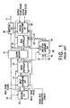
- the transmission signal processing circuit comprises a buffer memory 12 supplied with the input transmission signal 10.
- a deriving circuit 13 derives the input clock pulses and the input frame pulse from the input transmission signal 10.
- An input recognition circuit 14 is supplied with the input transmission signal 10 and with a plurality of signal rate information signals representative of the predetermined signal rates of the TU's of four sorts (namely, the TU-11, the TU-12, the TU-2, and the TU-3). Connected to the deriving circuit 13, the input recognition circuit 14 recognizes the TU of the input frame in response to the input clock pulses and the input frame pulse and with reference to the TU pointer of the input frame. The input recognition circuit 14 furthermore recognizes whether or not the TU of the input frame has a signal rate which corresponds to one of the predetermined signal rates represented by the signal rate information signals.
- the input recognition circuit 14 recognizes whether or not the TU of the input frame corresponds to one of the TU's of four sorts (namely, the TU-11, the TU-12, the TU-2, and the TU-3) with reference to the signal rate information signals.
- the input recognition circuit 14 recognizes that the TU of the input frame corresponds to one of the TU's of four sorts (namely, the TU-11, the TU-12, the TU-2, and the TU-3)
- the input recognition circuit 14 produces a location signal representative of a location of the TU in the input frame.
- a write controller 15 is connected to the deriving circuit 13 and the input recognition circuit 14.
- the write controller 15 controls writing of the TU of the input frame in the buffer memory 12 in response to the input clock pulses, the input frame pulse, and the location signal by supplying a write instruction signal 16 and a write address signal 17 to the buffer memory 12.
- the write controller 15 supplies the write instruction signal 16 and the write address signal 17 to the buffer memory 12 so that only the TU of the input frame is written in the buffer memory 12.
- a read controller 18 is supplied with the output clock pulses and the output frame pulse.
- the read controller 18 controls reading of the TU out of the buffer memory 12 in response to a stuff request signal 19 (which is either a positive stuff request signal 20 or a negative stuff request signal 21) by supplying a read address signal 23 and a read instruction signal 24 to the buffer memory 12.
- a stuff request signal 19 which is either a positive stuff request signal 20 or a negative stuff request signal 21
- the TU is read out of the buffer memory 12.
- a stuff execution judgement circuit 25 is given an input stuff threshold value 26 which is a combination of an input positive stuff threshold value 27 and an input negative stuff threshold value 28 which is greater than the input positive stuff threshold value 27.
- the stuff execution judgement circuit 25 judges whether or not a positive stuff operation should be executed by comparing a phase difference between the write address signal 17 and the read address signal 23 with the input positive stuff threshold value 27.
- the stuff execution judgement circuit 25 produces the positive stuff request signal 20 as the stuff request signal 19 when the stuff execution judgement circuit 25 judges that the positive stuff operation should be executed. More specifically, the stuff execution judgement circuit 25 produces the positive stuff request signal 20 when the phase difference is less than the input positive stuff threshold value 27. Responsive to the positive stuff request signal 20, the read controller 18 interrupts a reading operation to thereby increase the phase difference. As a result, a phase of an output signal of the buffer memory 12 becomes late.
- the stuff execution judgement circuit 25 furthermore judges whether or not a negative stuff operation should be executed by comparing the phase difference with the input negative stuff threshold value 28.
- the stuff execution judgement circuit 25 produces the negative stuff request signal 21 as the stuff request signal 19 when the stuff execution judgement circuit 25 judges that the negative stuff operation should be executed. More specifically, the stuff execution judgement circuit 25 produces the negative stuff request signal 21 when the phase difference is greater than the input negative stuff threshold value 28. Responsive to the negative stuff request signal 21, the read controller 18 carries out inverse control to decrease the phase difference.
- a pointer producing circuit 29 is supplied with the output clock pulses and the output frame pulse and supplied with the read address signal 23 and the read instruction signal 24 from the read controller 18. Further supplied with the locating signal from the input recognition circuit 14, the pointer producing circuit 29 produces the output pointer equivalent to the TU pointer which designates the location Z of the leading edge of the TU in the output frame of Fig. 2.
- An inserting circuit 30 is connected to the buffer memory 12 and the pointer producing circuit 29. The inserting circuit 30 inserts the output pointer in the output frame which includes the TU read out of the buffer memory 12. The inserting circuit 30 thereby produces the output transmission signal 11 which includes both the output pointer and the TU in the output frame.
- a combination of the pointer producing circuit 29 and the inserting circuit 30 is operable as an output transmission signal producing circuit. Supplied with the output clock pulses and the output frame pulse and connected to the buffer memory 12, the output transmission signal producing circuit produces the output transmission signal 11.
- the stuff execution judgement circuit 25 is given a constant input positive stuff threshold value 27 and a constant input negative stuff threshold value 28 no matter whether the TU of the input transmission signal 10 has any signal rate. That is, the input stuff threshold value 26 is constant or fixed for the TU's of four sorts (namely, the TU-11, the TU-12, the TU-2, and the TU-3). This results in an increase of a delay required from a write timing of the TU in the buffer memory 12 to a read timing of the TU under consideration out of the buffer memory 12 when the TU under consideration has a particular signal rate as mentioned above.
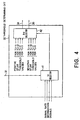
- the transmission signal processing circuit of Fig. 3 is similar to the transmission signal processing circuit of Fig. 1 expect for the following. That is, the input recognition circuit 14 of the transmission signal processing circuit of Fig. 3 further produces a sort signal 31 representative of a sort of the TU in the input frame.
- the transmission signal processing circuit of Fig. 3 further comprises a threshold determining circuit 32. Supplied with the signal rate information signals and connected to the input recognition circuit 14, the threshold determining circuit 32 determines in response to the sort signal 31 an optimum stuff threshold value 33 which is a combination of an optimum positive stuff threshold value 34 and an optimum negative stuff threshold value 35. The threshold determining circuit 32 thereby produces the optimum stuff threshold value 33 as the input stuff threshold value of the stuff execution judgement circuit 25.
- the threshold determining circuit 32 includes first and second selectors 41 and 42.
- the first selector 41 is given the signal rate information signals representative of the predetermined signal rates of the TU's of four sorts (namely, the TU-11, the TU-12, the TU-2, and the TU-3).
- the first selector 41 selects one of the signal rate information signals as a selected rate information signal.
- the above-mentioned one of the signal rate information signals corresponds to the sort of the TU that is represented by the sort signal 31.
- the second selector 42 is given a plurality of predetermined positive stuff threshold values in correspondence to the predetermined signal rates of the TU's of four sorts (namely, the TU-11, the TU-12, the TU-2, and the TU-3) and is also given a plurality of predetermined negative stuff threshold values in correspondence to the predetermined signal rates of the TU's of four sorts (namely, the TU-11, the TU-12, the TU-2, and the TU-3). That is, the second selector 42 is given the predetermined positive stuff threshold values for the TU-11, the TU-12, the TU-2, and the TU-3 and is also given the predetermined negative stuff threshold values for the TU-11, the TU-12, the TU-2, and the TU-3.
- the second selector 42 selects, as the optimum positive stuff threshold value 34 and the optimum negative stuff threshold value 35, one of the predetermined positive stuff threshold values for the TU-11, the TU-12, the TU-2, and the TU-3 and one of the predetermined negative stuff threshold values for the TU-11, the TU-12, the TU-2, and the TU-3.
- the above-mentioned one of the predetermined positive stuff threshold values and the above-mentioned one of the predetermined negative stuff threshold values correspond to the selected rate information signal produced by the first selector 41.
Landscapes
- Engineering & Computer Science (AREA)
- Computer Networks & Wireless Communication (AREA)
- Signal Processing (AREA)
- Computer Hardware Design (AREA)
- Time-Division Multiplex Systems (AREA)
- Synchronisation In Digital Transmission Systems (AREA)
Claims (4)
- Circuit de traitement de signal de transmission adapté pour recevoir un signal de transmission d'entrée (10) synchronisé avec des impulsions d'horloge d'entrée, ledit signal de transmission d'entrée comprenant une trame d'entrée qui est synchronisée avec une impulsion de trame d'entrée et qui comprend une unité tributaire, ledit circuit de traitement de signal de transmission étant, en outre, adapté pour recevoir des impulsions d'horloge de sortie et une impulsion de trame de sortie pour traiter ledit signal de transmission d'entrée en un signal de transmission de sortie (11) comprenant une trame de sortie comprenant ladite unité tributaire en transférant ladite unité tributaire de ladite trame d'entrée sur ladite trame de sortie du signal de transmission de sortie, ledit signal de transmission de sortie étant synchronisé avec lesdites impulsions d'horloge de sortie et ladite trame de sortie étant synchronisée avec ladite impulsion de trame de sortie, ledit circuit de traitement de signal de transmission comprenant : un circuit de déduction (13) pour déduire lesdites impulsions d'horloge d'entrée et ladite impulsion de trame d'entrée dudit signal de transmission d'entrée ; une mémoire (12) adaptée pour recevoir ledit signal de transmission d'entrée ; un circuit d'identification (14) adapté pour recevoir ledit signal de transmission d'entrée et connecté audit circuit de déduction pour identifier l'unité tributaire de ladite trame d'entrée en réponse auxdites impulsions d'horloge d'entrée et à ladite impulsion de trame d'entrée afin de produire un signal de localisation représentatif d'un emplacement de ladite unité tributaire dans ladite trame d'entrée ; un contrôleur d'écriture (15) connecté audit circuit de déduction et audit circuit d'identification pour contrôler l'écriture de l'unité tributaire de ladite trame d'entrée dans ladite mémoire en réponse auxdites impulsions d'horloge d'entrée, à ladite impulsion de trame d'entrée et audit signal de localisation en délivrant un signal d'adresse d'écriture (17) à ladite mémoire ; un contrôleur de lecture (18) adapté pour recevoir lesdites impulsions d'horloge de sortie et ladite impulsion de trame de sortie pour contrôler la lecture de ladite unité tributaire dans ladite mémoire en réponse à un signal de requête de remplissage (19) en délivrant un signal d'adresse de lecture (23) à ladite mémoire ; un circuit de jugement d'exécution de remplissage (25) qui a reçu une valeur de seuil de remplissage d'entrée et connecté audit contrôleur d'écriture et audit contrôleur de lecture pour juger si, oui ou non, une opération de remplissage devrait être exécutée en comparant une différence entre ledit signal d'adresse d'écriture et ledit signal d'adresse de lecture avec ladite valeur de seuil de remplissage d'entrée, ledit circuit de jugement d'exécution de remplissage produisant ledit signal de requête de remplissage lorsque ledit circuit de jugement d'exécution de remplissage juge que ladite opération de remplissage devrait être exécutée ; et un circuit de génération de signal de transmission de sortie (29, 30) recevant lesdites impulsions d'horloge de sortie et ladite impulsion de trame de sortie et connecté à ladite mémoire pour générer ledit signal de transmission de sortie ; caractérisé en ce que :ledit circuit d'identification est adapté pour générer un signal de tri (31) représentatif d'un tri de l'unité tributaire dans ladite trame d'entrée ; etledit circuit de traitement de signal de transmission comprend en outre :un circuit de détermination de seuil (32) connecté audit circuit d'identification pour déterminer une valeur de seuil de remplissage optimale (33) en réponse audit signal de tri afin de générer ladite valeur de seuil de remplissage optimale en tant que dite valeur de seuil de remplissage d'entrée.
- Circuit de traitement de signal de transmission selon la revendication 1, l'unité tributaire ayant l'une d'une pluralité de fréquences de signal prédéterminées dans ladite trame d'entrée, dans lequel ledit circuit de détermination de seuil comprend :un premier sélecteur (41) qui a reçu une pluralité de signaux d'information de fréquence de signal représentatifs desdites fréquences de signal prédéterminées et connecté audit circuit d'identification pour sélectionner l'un desdits signaux d'information de fréquence de signal en tant que signal d'information de fréquence sélectionné, ledit un des signaux d'information de fréquence de signal correspondant au tri de ladite unité tributaire qui est représenté par ledit signal de tri ; etun deuxième sélecteur (42) qui a reçu une pluralité de valeurs de seuil de remplissage prédéterminées correspondant auxdites fréquences de signal prédéterminées et connecté audit premier sélecteur pour sélectionner l'une desdites valeurs de seuil de remplissage prédéterminées en tant que dite valeur de seuil de remplissage optimale, ladite une des valeurs de seuil de remplissage prédéterminées correspondant audit signal d'information de fréquence sélectionné.
- Circuit de traitement de signal de transmission selon la revendication 1, ledit circuit de jugement d'exécution de remplissage recevant une valeur de seuil de remplissage positive d'entrée et une valeur de seuil de remplissage négative d'entrée en tant que dite valeur de seuil de remplissage d'entrée, ledit circuit de jugement d'exécution de remplissage jugeant si, oui ou non, une opération de remplissage positive devrait être exécutée en comparant ladite différence avec ladite valeur de seuil de remplissage positive d'entrée, ledit circuit de jugement d'exécution de remplissage générant un signal de requête de remplissage positive (20) en tant que dit signal de requête de remplissage lorsque ledit circuit de jugement d'exécution de remplissage juge que ladite opération de remplissage positive devrait être exécutée, ledit circuit de jugement d'exécution de remplissage jugeant si, oui ou non, une opération de remplissage négative devrait être exécutée en comparant ladite différence avec ladite valeur de seuil de remplissage négative d'entrée, ledit circuit de jugement d'exécution de remplissage générant un signal de requête de remplissage négative (21) en tant que dit signal de requête de remplissage lorsque ledit circuit de jugement d'exécution de remplissage juge que ladite opération de remplissage négative devrait être exécutée,
dans lequel ledit circuit de détermination de seuil est adapté pour déterminer une valeur de seuil de remplissage positive optimale (34) et une valeur de seuil de remplissage négative optimale (35) en tant que dite valeur de seuil de remplissage optimale en réponse audit signal de tri afin de produire ladite valeur de seuil de remplissage positive optimale et ladite valeur de seuil de remplissage négative optimale en tant que dite valeur de seuil de remplissage positive d'entrée et dite valeur de seuil de remplissage négative d'entrée. - Circuit de traitement de signal de transmission selon la revendication 3, l'unité tributaire ayant l'une d'une pluralité de fréquences de signal prédéterminées dans ladite trame d'entrée, dans lequel ledit circuit de détermination de seuil comprend :un premier sélecteur (41) qui a reçu une pluralité de signaux d'information de fréquence de signal représentatifs desdites fréquences de signal prédéterminées et connecté audit circuit d'identification pour sélectionner l'un desdits signaux d'information de fréquence de signal en tant que signal d'information de fréquence sélectionné, ledit un des signaux d'information de fréquence de signal correspondant au tri de ladite unité tributaire qui est représenté par ledit signal de tri ; etun deuxième sélecteur (42) qui a reçu une pluralité de valeurs de seuil de remplissage positives prédéterminées en correspondance avec lesdites fréquences de signal prédéterminées et une pluralité de valeurs de seuil de remplissage négatives prédéterminées en correspondance avec lesdites fréquences de signal prédéterminées et connecté audit premier sélecteur pour sélectionner l'une desdites valeurs de seuil de remplissage positives prédéterminées en tant que dite valeur de seuil de remplissage positive optimale et l'une desdites valeurs de seuil de remplissage négatives prédéterminées en tant que dite valeur de seuil de remplissage négative optimale, ladite une des valeurs de seuil de remplissage positives prédéterminées et ladite une des valeurs de seuil de remplissage négatives prédéterminées correspondant audit signal d'information de fréquence sélectionné.
Applications Claiming Priority (3)
| Application Number | Priority Date | Filing Date | Title |
|---|---|---|---|
| JP6326305A JP2616731B2 (ja) | 1994-12-27 | 1994-12-27 | 伝送信号処理回路 |
| JP32630594 | 1994-12-27 | ||
| JP326305/94 | 1994-12-27 |
Publications (3)
| Publication Number | Publication Date |
|---|---|
| EP0720320A2 EP0720320A2 (fr) | 1996-07-03 |
| EP0720320A3 EP0720320A3 (fr) | 1998-07-29 |
| EP0720320B1 true EP0720320B1 (fr) | 2004-03-17 |
Family
ID=18186286
Family Applications (1)
| Application Number | Title | Priority Date | Filing Date |
|---|---|---|---|
| EP95120568A Expired - Lifetime EP0720320B1 (fr) | 1994-12-27 | 1995-12-27 | Circuit de traitement d'un signal transmis pouvant déterminer la valeur optimale du seuil de justification selon le genre d'unité tributaire du signal d'entrée |
Country Status (6)
| Country | Link |
|---|---|
| US (1) | US5642357A (fr) |
| EP (1) | EP0720320B1 (fr) |
| JP (1) | JP2616731B2 (fr) |
| CA (1) | CA2166139C (fr) |
| DE (1) | DE69532705T2 (fr) |
| MY (1) | MY111859A (fr) |
Families Citing this family (10)
| Publication number | Priority date | Publication date | Assignee | Title |
|---|---|---|---|---|
| US5841762A (en) * | 1996-03-29 | 1998-11-24 | British Telecommunications Public Limited Company | Monitoring a synchronous digital hierarchy transmission path |
| DE19732943A1 (de) * | 1997-07-31 | 1999-02-04 | Alsthom Cge Alcatel | Verfahren und Komponente zum Ausgleich von Frequenz- und Phasenschwankungen |
| US6229863B1 (en) | 1998-11-02 | 2001-05-08 | Adc Telecommunications, Inc. | Reducing waiting time jitter |
| JP2003078497A (ja) * | 2001-09-04 | 2003-03-14 | Fujitsu Ltd | 伝送装置 |
| JP3970581B2 (ja) | 2001-11-09 | 2007-09-05 | 富士通株式会社 | 伝送装置および伝送システム |
| US7839887B1 (en) * | 2003-10-16 | 2010-11-23 | Network Equipment Technologies, Inc. | Method and system for providing frame rate adaption |
| JP2006270792A (ja) * | 2005-03-25 | 2006-10-05 | Fujitsu Ltd | フレーム伝送方法及び装置 |
| US7839885B2 (en) * | 2005-04-25 | 2010-11-23 | Lsi Corporation | Connection memory for tributary time-space switches |
| JP4729049B2 (ja) * | 2005-12-22 | 2011-07-20 | 日本電信電話株式会社 | 光送信器 |
| US8681917B2 (en) | 2010-03-31 | 2014-03-25 | Andrew Llc | Synchronous transfer of streaming data in a distributed antenna system |
Family Cites Families (8)
| Publication number | Priority date | Publication date | Assignee | Title |
|---|---|---|---|---|
| CA1262173A (fr) * | 1986-05-29 | 1989-10-03 | James Angus Mceachern | Synchronisation de signaux de donnees asynchrones |
| JP2782731B2 (ja) * | 1988-09-19 | 1998-08-06 | 日本電気株式会社 | 同期多重化網の回線乗換え方式及び回線乗換えに用いられる演算回路 |
| LU87714A1 (de) * | 1989-11-29 | 1990-07-24 | Siemens Ag | Verfahren zum uebertragen eines digitalen breitbandsignals in einer untersystemeinheitenkette ueber ein netz einer synchron-digital-multiplexhierarchie |
| DE4013317A1 (de) * | 1990-04-26 | 1990-08-23 | Ant Nachrichtentech | Stopfverfahren zur reduktion des wartezeitjitters und anordnung zur durchfuehrung des verfahrens |
| US5263057A (en) * | 1990-05-09 | 1993-11-16 | Ant Nachrichtentechnik Gmbh | Method of reducing waiting time jitter |
| US5276688A (en) * | 1990-06-09 | 1994-01-04 | U.S. Philips Corporation | Circuit arrangement for bit rate adjustment |
| US5331641A (en) * | 1990-07-27 | 1994-07-19 | Transwitch Corp. | Methods and apparatus for retiming and realignment of STS-1 signals into STS-3 type signal |
| DE4108429A1 (de) * | 1991-03-15 | 1992-09-17 | Philips Patentverwaltung | Uebertragungssystem fuer die digitale synchrone hierarchie |
-
1994
- 1994-12-27 JP JP6326305A patent/JP2616731B2/ja not_active Expired - Fee Related
-
1995
- 1995-12-27 US US08/578,079 patent/US5642357A/en not_active Expired - Lifetime
- 1995-12-27 DE DE69532705T patent/DE69532705T2/de not_active Expired - Lifetime
- 1995-12-27 EP EP95120568A patent/EP0720320B1/fr not_active Expired - Lifetime
- 1995-12-27 CA CA002166139A patent/CA2166139C/fr not_active Expired - Fee Related
- 1995-12-27 MY MYPI95004115A patent/MY111859A/en unknown
Also Published As
| Publication number | Publication date |
|---|---|
| MY111859A (en) | 2001-01-31 |
| EP0720320A3 (fr) | 1998-07-29 |
| JP2616731B2 (ja) | 1997-06-04 |
| CA2166139C (fr) | 1999-02-23 |
| CA2166139A1 (fr) | 1996-06-28 |
| DE69532705T2 (de) | 2004-08-05 |
| US5642357A (en) | 1997-06-24 |
| JPH08186556A (ja) | 1996-07-16 |
| DE69532705D1 (de) | 2004-04-22 |
| EP0720320A2 (fr) | 1996-07-03 |
Similar Documents
| Publication | Publication Date | Title |
|---|---|---|
| US5210745A (en) | Frame restructuring interface for digital bit streams multiplexed by time-division multiplexing digital tributaries with different bit rates | |
| EP0459686B1 (fr) | Synchronisation d'un signal numérique utilisant une mémoire élastique | |
| US5359605A (en) | Circuit arrangement for adjusting the bit rates of two signals | |
| EP0529012B1 (fr) | Procede et circuit de synchronisation de donnees | |
| US4543652A (en) | Time-division switching unit | |
| EP0720320B1 (fr) | Circuit de traitement d'un signal transmis pouvant déterminer la valeur optimale du seuil de justification selon le genre d'unité tributaire du signal d'entrée | |
| EP0559649A1 (fr) | Procede et appareil pour transferer une charge utile de donnes provenant d'un premier signal de reseau optique pratiquement synchone (sonet) vers un signal de sonet ayant une frequence differente | |
| US5563877A (en) | Telecommunication network node | |
| US4920547A (en) | Stuff synchronization circuit | |
| US5515362A (en) | Digital signal transmission apparatus | |
| EP0584636B1 (fr) | Détecteur de phase pour une memoire élastique | |
| US7639673B2 (en) | Method and apparatus for SDH/SONET frame alignment | |
| EP0699363B1 (fr) | Procede et dispositif permettant la prise d'une decision de justification au niveau d'un systeme de telecommunication numerique | |
| JPH0621929A (ja) | 伝送装置および等化回路装置 | |
| US5357515A (en) | Non-interruption transmission line switching system in a duplex transmission network | |
| US5923669A (en) | Adaptive boundary buffers | |
| WO1994003023A1 (fr) | Procede de mise en oeuvre d'une commutation temporelle et commutateur temporel | |
| EP1073226B1 (fr) | Procédé de mise en correspondance d'affluents dans des trames temporelles dans des réseaux de télécommunication et circuit correspondant | |
| JP3198675B2 (ja) | データレート変換装置 | |
| KR0168921B1 (ko) | 동기식 전송시스템에서 시험액세스를 위한 24x3교차 스위치 회로 | |
| JP3010634B2 (ja) | フレーム同期多重処理方式 | |
| JPH04322525A (ja) | 同期ディジタルハイアラーキにおけるポインタ値発生方法 | |
| HK1011821B (en) | Method for implementing time switching and a time switch | |
| JPH0670384A (ja) | クロスコネクト装置 |
Legal Events
| Date | Code | Title | Description |
|---|---|---|---|
| PUAI | Public reference made under article 153(3) epc to a published international application that has entered the european phase |
Free format text: ORIGINAL CODE: 0009012 |
|
| AK | Designated contracting states |
Kind code of ref document: A2 Designated state(s): DE FR SE |
|
| PUAL | Search report despatched |
Free format text: ORIGINAL CODE: 0009013 |
|
| AK | Designated contracting states |
Kind code of ref document: A3 Designated state(s): DE FR SE |
|
| 17P | Request for examination filed |
Effective date: 19980623 |
|
| 17Q | First examination report despatched |
Effective date: 20021106 |
|
| GRAP | Despatch of communication of intention to grant a patent |
Free format text: ORIGINAL CODE: EPIDOSNIGR1 |
|
| GRAS | Grant fee paid |
Free format text: ORIGINAL CODE: EPIDOSNIGR3 |
|
| GRAA | (expected) grant |
Free format text: ORIGINAL CODE: 0009210 |
|
| AK | Designated contracting states |
Kind code of ref document: B1 Designated state(s): DE FR SE |
|
| REG | Reference to a national code |
Ref country code: SE Ref legal event code: TRGR |
|
| REF | Corresponds to: |
Ref document number: 69532705 Country of ref document: DE Date of ref document: 20040422 Kind code of ref document: P |
|
| ET | Fr: translation filed | ||
| PLBE | No opposition filed within time limit |
Free format text: ORIGINAL CODE: 0009261 |
|
| STAA | Information on the status of an ep patent application or granted ep patent |
Free format text: STATUS: NO OPPOSITION FILED WITHIN TIME LIMIT |
|
| 26N | No opposition filed |
Effective date: 20041220 |
|
| PGFP | Annual fee paid to national office [announced via postgrant information from national office to epo] |
Ref country code: SE Payment date: 20081205 Year of fee payment: 14 |
|
| EUG | Se: european patent has lapsed | ||
| PG25 | Lapsed in a contracting state [announced via postgrant information from national office to epo] |
Ref country code: SE Free format text: LAPSE BECAUSE OF NON-PAYMENT OF DUE FEES Effective date: 20091228 |
|
| PGFP | Annual fee paid to national office [announced via postgrant information from national office to epo] |
Ref country code: DE Payment date: 20131224 Year of fee payment: 19 |
|
| PGFP | Annual fee paid to national office [announced via postgrant information from national office to epo] |
Ref country code: FR Payment date: 20131209 Year of fee payment: 19 |
|
| REG | Reference to a national code |
Ref country code: DE Ref legal event code: R119 Ref document number: 69532705 Country of ref document: DE |
|
| REG | Reference to a national code |
Ref country code: FR Ref legal event code: ST Effective date: 20150831 |
|
| PG25 | Lapsed in a contracting state [announced via postgrant information from national office to epo] |
Ref country code: DE Free format text: LAPSE BECAUSE OF NON-PAYMENT OF DUE FEES Effective date: 20150701 |
|
| PG25 | Lapsed in a contracting state [announced via postgrant information from national office to epo] |
Ref country code: FR Free format text: LAPSE BECAUSE OF NON-PAYMENT OF DUE FEES Effective date: 20141231 |