EP0720779B1 - Elektronentransfereffektanordnung - Google Patents
Elektronentransfereffektanordnung Download PDFInfo
- Publication number
- EP0720779B1 EP0720779B1 EP95922698A EP95922698A EP0720779B1 EP 0720779 B1 EP0720779 B1 EP 0720779B1 EP 95922698 A EP95922698 A EP 95922698A EP 95922698 A EP95922698 A EP 95922698A EP 0720779 B1 EP0720779 B1 EP 0720779B1
- Authority
- EP
- European Patent Office
- Prior art keywords
- region
- effect device
- anode
- active region
- electron effect
- Prior art date
- Legal status (The legal status is an assumption and is not a legal conclusion. Google has not performed a legal analysis and makes no representation as to the accuracy of the status listed.)
- Expired - Lifetime
Links
- 230000000694 effects Effects 0.000 title claims description 70
- 239000004065 semiconductor Substances 0.000 claims description 30
- GPXJNWSHGFTCBW-UHFFFAOYSA-N Indium phosphide Chemical compound [In]#P GPXJNWSHGFTCBW-UHFFFAOYSA-N 0.000 claims description 24
- 239000000463 material Substances 0.000 claims description 20
- 230000004888 barrier function Effects 0.000 claims description 19
- 229910000530 Gallium indium arsenide Inorganic materials 0.000 claims description 17
- 239000000758 substrate Substances 0.000 claims description 12
- 238000000034 method Methods 0.000 claims description 7
- 125000006850 spacer group Chemical group 0.000 claims description 7
- 238000005036 potential barrier Methods 0.000 claims description 6
- AUCDRFABNLOFRE-UHFFFAOYSA-N alumane;indium Chemical compound [AlH3].[In] AUCDRFABNLOFRE-UHFFFAOYSA-N 0.000 claims description 4
- 238000004519 manufacturing process Methods 0.000 claims description 4
- GYHNNYVSQQEPJS-UHFFFAOYSA-N Gallium Chemical compound [Ga] GYHNNYVSQQEPJS-UHFFFAOYSA-N 0.000 claims description 3
- 230000007423 decrease Effects 0.000 claims description 3
- 229910052733 gallium Inorganic materials 0.000 claims description 3
- 230000002401 inhibitory effect Effects 0.000 claims description 3
- 239000002019 doping agent Substances 0.000 description 17
- 230000001133 acceleration Effects 0.000 description 7
- 230000008859 change Effects 0.000 description 7
- 239000000203 mixture Substances 0.000 description 7
- 238000012546 transfer Methods 0.000 description 6
- 239000002800 charge carrier Substances 0.000 description 5
- 230000006872 improvement Effects 0.000 description 5
- JBRZTFJDHDCESZ-UHFFFAOYSA-N AsGa Chemical compound [As]#[Ga] JBRZTFJDHDCESZ-UHFFFAOYSA-N 0.000 description 4
- 229910001218 Gallium arsenide Inorganic materials 0.000 description 4
- 238000005452 bending Methods 0.000 description 4
- 238000005530 etching Methods 0.000 description 4
- 229910052751 metal Inorganic materials 0.000 description 4
- 239000002184 metal Substances 0.000 description 4
- 239000007787 solid Substances 0.000 description 4
- 238000009825 accumulation Methods 0.000 description 3
- 238000002347 injection Methods 0.000 description 3
- 239000007924 injection Substances 0.000 description 3
- 230000008569 process Effects 0.000 description 3
- 230000009467 reduction Effects 0.000 description 3
- 229910000673 Indium arsenide Inorganic materials 0.000 description 2
- 238000001816 cooling Methods 0.000 description 2
- 238000009792 diffusion process Methods 0.000 description 2
- 230000005684 electric field Effects 0.000 description 2
- 238000012986 modification Methods 0.000 description 2
- 230000004048 modification Effects 0.000 description 2
- 229910052709 silver Inorganic materials 0.000 description 2
- 239000004332 silver Substances 0.000 description 2
- 229910000980 Aluminium gallium arsenide Inorganic materials 0.000 description 1
- XUIMIQQOPSSXEZ-UHFFFAOYSA-N Silicon Chemical group [Si] XUIMIQQOPSSXEZ-UHFFFAOYSA-N 0.000 description 1
- KXNLCSXBJCPWGL-UHFFFAOYSA-N [Ga].[As].[In] Chemical compound [Ga].[As].[In] KXNLCSXBJCPWGL-UHFFFAOYSA-N 0.000 description 1
- MDPILPRLPQYEEN-UHFFFAOYSA-N aluminium arsenide Chemical compound [As]#[Al] MDPILPRLPQYEEN-UHFFFAOYSA-N 0.000 description 1
- 230000015572 biosynthetic process Effects 0.000 description 1
- 150000001875 compounds Chemical class 0.000 description 1
- 238000013461 design Methods 0.000 description 1
- 238000010438 heat treatment Methods 0.000 description 1
- 239000012535 impurity Substances 0.000 description 1
- 229910052738 indium Inorganic materials 0.000 description 1
- APFVFJFRJDLVQX-UHFFFAOYSA-N indium atom Chemical compound [In] APFVFJFRJDLVQX-UHFFFAOYSA-N 0.000 description 1
- 238000002488 metal-organic chemical vapour deposition Methods 0.000 description 1
- 238000001451 molecular beam epitaxy Methods 0.000 description 1
- 238000007747 plating Methods 0.000 description 1
- 238000012545 processing Methods 0.000 description 1
- 230000002035 prolonged effect Effects 0.000 description 1
- 238000000926 separation method Methods 0.000 description 1
- 238000011282 treatment Methods 0.000 description 1
- 230000005533 two-dimensional electron gas Effects 0.000 description 1
Images
Classifications
-
- H—ELECTRICITY
- H10—SEMICONDUCTOR DEVICES; ELECTRIC SOLID-STATE DEVICES NOT OTHERWISE PROVIDED FOR
- H10N—ELECTRIC SOLID-STATE DEVICES NOT OTHERWISE PROVIDED FOR
- H10N80/00—Bulk negative-resistance effect devices
- H10N80/10—Gunn-effect devices
- H10N80/107—Gunn diodes
-
- H—ELECTRICITY
- H01—ELECTRIC ELEMENTS
- H01S—DEVICES USING THE PROCESS OF LIGHT AMPLIFICATION BY STIMULATED EMISSION OF RADIATION [LASER] TO AMPLIFY OR GENERATE LIGHT; DEVICES USING STIMULATED EMISSION OF ELECTROMAGNETIC RADIATION IN WAVE RANGES OTHER THAN OPTICAL
- H01S5/00—Semiconductor lasers
- H01S5/20—Structure or shape of the semiconductor body to guide the optical wave ; Confining structures perpendicular to the optical axis, e.g. index or gain guiding, stripe geometry, broad area lasers, gain tailoring, transverse or lateral reflectors, special cladding structures, MQW barrier reflection layers
- H01S5/2004—Confining in the direction perpendicular to the layer structure
- H01S5/2009—Confining in the direction perpendicular to the layer structure by using electron barrier layers
-
- H—ELECTRICITY
- H01—ELECTRIC ELEMENTS
- H01S—DEVICES USING THE PROCESS OF LIGHT AMPLIFICATION BY STIMULATED EMISSION OF RADIATION [LASER] TO AMPLIFY OR GENERATE LIGHT; DEVICES USING STIMULATED EMISSION OF ELECTROMAGNETIC RADIATION IN WAVE RANGES OTHER THAN OPTICAL
- H01S5/00—Semiconductor lasers
- H01S5/30—Structure or shape of the active region; Materials used for the active region
- H01S5/32—Structure or shape of the active region; Materials used for the active region comprising PN junctions, e.g. hetero- or double- heterostructures
- H01S5/3211—Structure or shape of the active region; Materials used for the active region comprising PN junctions, e.g. hetero- or double- heterostructures characterised by special cladding layers, e.g. details on band-discontinuities
- H01S5/3215—Structure or shape of the active region; Materials used for the active region comprising PN junctions, e.g. hetero- or double- heterostructures characterised by special cladding layers, e.g. details on band-discontinuities graded composition cladding layers
Definitions
- This invention relates to a transferred electron effect device.
- US-A-4,801,982 describes a transferred electron effect device comprising a semiconductor body having an active region of n conductivity type formed of a material having a relatively low mass, high mobility conduction band main minimum and at least one relatively high mass, low mobility conduction band satellite minimum and an injector region defining a potential barrier to the flow of electrons into the active region of a height such that, in operation of the device, electrons with sufficient energy to surmount the barrier provided by the injector region are emitted into the active region with an energy comparable to that of the at least one relatively high mass, low mobility conduction band satellite minimum.
- the injector region is intended to enable electrons with an energy comparable to that of a conduction band satellite minimum to be injected into the active region, so avoiding, or at least reducing the extent of, any acceleration or dead zone within the active region. This reduction of the acceleration or dead zone should result in an improvement in the rf (radio frequency) output power and efficiency of the transferred electron effect device.
- the transferred electron effect device described in US Patent No.4,801,982 has an active region which may be formed from gallium arsenide or indium phosphide and the injector region is in the form of a graded band gap injector region comprising a varying composition of aluminium gallium arsenide or indium aluminium arsenide.
- the graded band gap injector region is intended to allow an improvement in the power and efficiency of the transferred electron device by allowing the accumulation or dipole layer to start as close as possible to the cathode region.
- a relatively highly doped region separates the injector region from the active region to inhibit the spread of the depletion region into the relatively lowly doped active region.
- this highly doped region tends to cause band bending which pulls the conduction band in the active region down adjacent the injector region and so causes the energy with which electrons are emitted into the active region to fall so that a or a larger acceleration zone will be required within the active region for the electrons to gain sufficient energy to transfer to a conduction band satellite minimum.
- the inclusion of this highly doped region thus detrimentally affects the performance and efficiency of the device.
- the present invention provides a transferred electron effect device comprising a semiconductor body having an active region of n conductivity type formed of a material having a relatively low mass, high mobility conduction band main minimum and at least one relatively high mass, low mobility conduction band satellite minimum and an injector region defining a potential barrier to the flow of electrons into the active region of a height such that, in operation of the device, electrons with sufficient energy to surmount the barrier provided by the injector region are emitted into the active region with an energy comparable to that of the at least one relatively high mass, low mobility conduction band satellite minimum, characterised in that an electron-containing well region of a material different from that of the active region and of the injector region is provided between the injector region and the active region for inhibiting the spread of a depletion region into the active region during operation of the device.
- a well region inhibits the spread of the depletion region into the active region during operation of the device without the significant conduction band bending which might otherwise arise.
- the use of a well region to inhibit the spread of the depletion region enables the difference in conduction band energies between the injector region and the active region to be maintained so enabling electrons to be injected into the active region with high energy which, as noted above, should facilitate improved performance.
- the injector region may be any suitable injector region, for example an injector region of the type described and claimed in our US Patent No. 5,258,624 or a graded band gap injector region of the type mentioned above.
- the graded band gap injector region may comprise gallium aluminium indium phosphide, for example, Ga 0.48x Al 0.48(1-x) In 0.52 As, where x decreases from 1 to 0 in a direction away from the cathode region.
- the well region may be formed of n conductivity type semiconductor material.
- the well region may comprise n conductivity gallium indium arsenide where the active region comprises indium phosphide.
- the well region may be modulation-doped by a relatively highly doped semiconductor modulation region doped so as to be n conductivity type and spacing the well region from the active region.
- the use of a modulation-doped well region has additional advantages in that the doping of the modulation region is independent of the width of the well. This enables the doping level in the modulation region to be lower than that used where the well itself is doped because the modulation region can be thinner than the well region. Accordingly, the Fermi level can be much lower, thereby enabling the energy at which electrons are emitted over the potential barrier defined by the injector region to be increased, so making it even more likely that electrons emitted over the barrier provided by the graded band gap injector will be transferred directly to a satellite conduction band minimum. This should result in a transferred electron effect device having an even better rf output power and efficiency.
- the modulation region may be spaced from the well region by an intrinsic spacer region formed of the same semiconductor as the modulation region.
- the well region may comprise gallium indium arsenide and the modulation region may comprise indium phosphide.
- the device may comprise anode and cathode semiconductor regions spaced apart by the active region and each comprising semiconductor regions highly doped so as to be n conductivity type and anode and cathode electrodes contacting the anode and cathode regions, respectively, and in this case the anode and cathode regions may comprise highly n conductivity type gallium indium arsenide regions forming ohmic contacts with the anode and cathode electrodes, respectively.
- a heat sink region may be provided on an exposed surface of the anode region for removing heat dissipated in the device. As described and claimed in our US Patent No. 5,250,815, this should result in a further improvement in performance.
- a method of manufacturing the transferred electron effect device comprises providing a semiconductor substrate, providing an epitaxial layer structure on the substrate to define a semiconductor body comprising an anode region formed on the substrate and the active and cathode regions, characterised by, after defining the semiconductor body, selectively removing the substrate to expose a surface of the anode region and then providing a heat sink region on the exposed surface of the anode region for removing heat dissipated in the epitaxial layer structure.
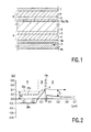
- Figures 1 to 5 illustrate examples of transferred electron effect devices 1 each comprising a semiconductor body 2 having an active region 6 of n conductivity type formed of a material having a relatively low mass, high mobility conduction band main minimum and at least one relatively high mass, low mobility conduction band satellite minimum and an injector region 9 defining a potential barrier P to the flow of electrons into the active region 6 of a height such that, in operation of the device, electrons with sufficient energy to surmount the barrier P provided by the injector region 9 are emitted into the active region 6 with an energy comparable to that of the at least one relatively high mass, low mobility conduction band satellite minimum.
- an electron-containing well region 10a, 10b of a material different from that of the active region 6 and of the injector region 9 is provided between the injector region 9 and the active region 6 for inhibiting the spread of a depletion region into the active region 6 during operation of the device.
- a well region more commonly a quantum well region, for electrons is a region of one material which is sandwiched between barrier regions of different material that have a conduction band energy greater than that of the one material so that electrons are trapped in confined states within the well region and which is sufficiently thin that the confined state energy levels within the well region are quantised.
- a well region for electrons will also form a well region for holes and will thus have a valence band energy lower (ie of higher hole energy) than that of the barrier regions.
- electron-containing well region as used herein should be understood to mean a well region which is either directly doped so as to be of n conductivity type or is modulation-doped from an n conductivity type modulation layer or is otherwise caused to contain electrons.
- the well region 10a, 10b should be sufficiently thin to allow the passage of hot charge carriers, that is charge carriers with an energy above the Fermi level of the active region 6, to pass without significant cooling or thermalisation yet sufficiently thick that the lowest confined state energy level is not significantly raised above the minimum energy point within the well region 10a.
- an electron-containing well region 10a, 10b inhibits the spread of the depletion region into the active region 6 during operation of the device without the significant conduction band bending which might otherwise arise if a depletion region stop in the form of a highly doped region of the same material as the active region were used.
- the difference in conduction band energies between the injector region 9 and the active region 6 is thus maintained so enabling electrons to be injected into the active region 6 with an energy comparable to that of a conduction band satellite minimum.
- the need for any dead space or acceleration zone in the active region 6 is removed or at least reduced which should facilitate improved performance.
- a transferred electron effect device 1 having a semiconductor body 2 comprising an active region 6 comprising indium phosphide doped so as to be n conductivity type, anode and cathode semiconductor regions A and K spaced apart by the active region 6 and each comprising semiconductor regions highly doped so as to be n conductivity type and anode and cathode electrodes 4 and 7 contacting the anode and cathode regions A and K.
- the anode and cathode regions A and K comprise highly n conductivity type gallium indium arsenide regions 5 and 8 forming ohmic contacts with the anode and cathode electrodes 4 and 7, respectively.
- the injector region is in the form of a graded band gap injector region 9 and forms part of the cathode region K.
- the graded band gap injector region 9 is formed of a suitable III-V semiconductor compound which separates the active region 6 from the gallium indium arsenide contact region 8.
- the semiconductor material is gallium aluminium indium arsenide with the composition: Ga 0.48x Al 0.48(1-x) In 0.52 As, where x decreases from 1 to 0 in a direction away from the contact region 8.
- graded band gap injector region 9 enables an improvement in the power and efficiency of the transferred electron effect device by allowing, in operation of the device, the accumulation or dipole layer to start within the active region 6 as close as possible to the cathode region K.
- the gallium indium arsenide contact regions 5 and 8 have the composition Ga 0.47 In 0.53 As so that the contact region 8 provides a lattice match to the graded band gap injector region 9 which will, in this example, have the composition Ga 0.47 In 0.53 As adjacent the contact region 8.
- the anode region A comprises the highly doped gallium indium arsenide contact region 5 and a highly doped indium phosphide region 3 separating the contact region 5 from the active region 3.
- the electron-containing well region 10a is in this example formed of n conductivity type gallium indium arsenide again with the composition Ga 0.47 In 0.53 As so as to provide a lattice match to the adjoining injector and active regions 9 and 6.
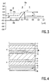
- Figure 2 illustrates schematically the energy level in electron volts (eV) across the area around the active region 6 of one example of a transferred electron effect device 1a having the structure shown in Figure 1.
- the solid line 20a in Figure 2 illustrates the conduction band energy when no voltages are applied to the cathode and anode electrodes 4 and 7 while the dashed line 21a illustrates the change in the conduction band energy level when a forward-biasing voltage of 30 volts is applied between the cathode and anode electrodes 4 and 7.
- the dotted line 22a represents the applied forward-biasing voltage Vf.
- the Fermi level is defined as the zero level in Figure 2.
- the cathode contact region 8 has a thickness of 0.25 ⁇ m and is doped to a concentration of 5x10 18 atoms cm -3 with a suitable n conductivity type dopant, for example silicon atoms.
- the graded band gap injector region 9 is 0.1 ⁇ m thick and is intrinsic, that is not intentionally doped, having in practice a net n conductivity dopant concentration of about 10 16 atoms cm -3 .
- the active region 6 has a thickness of 1.1 ⁇ m and has a doping concentration of about 10 16 atoms cm -3 , that is it is not intentionally doped.
- the well region 10a is 10nm (nanometres) thick and is doped so as to be of n conductivity type with a dopant concentration of 2x10 18 atoms cm -3 .
- the indium phosphide active region 6 and the graded band gap injector region 9 form the barrier regions of the well region.
- electrons emitted into the active region must have or acquire sufficient energy to transfer from the relatively low mass, high mobility conduction band main minimum to a relatively high mass, low mobility conduction band satellite minimum within the active region 6.
- the graded band gap injector region 9 defines a potential barrier P so that only electrons with sufficient energy can pass over the barrier to enter the active region 6.
- the barrier height provided by the graded band gap injector region 9 and thus the energy at which electrons are emitted over the barrier is determined by the difference between the Fermi level in the active region 6 and the highest point of the barrier P.
- the sum of the energy E i at which electrons are emitted over the barrier P and of the energy separation between the conduction band edge and Fermi level of the active region 6 should not exceed the energy difference between the conduction band main minimum and the satellite minima in the active region 6.
- the energy difference between the conduction band main minimum and the satellite minima is 0.53eV.
- the ramp in the conduction band provided by the graded band gap injector region 9 should, as indicated by the solid line 20a in Figure 2, form the largest resistance within the structure so that almost all the applied bias will fall across the graded band gap injector region 9.
- the ramp in the conduction band caused by the graded band gap injector region 9 should have been almost flattened and the extra bias falls across the active region 6. This flattening changes the field within the transferred electron effect device and it is important to ensure that this change in field does not start to deplete part of the active or drift region 9.
- the amount of doping required to enable the well region 10a to inhibit the spread of the depletion region into the active region 6 may be estimated.
- the electric field within the transferred electron effect device resulting from the graded band gap region 9 is approximately ⁇ E c /L where ⁇ E c is the conduction band offset between the gallium indium arsenide of the well region 10a and the aluminium indium arsenide of the graded band gap injector region 9 (about 0.52eV) and L is the distance over which the grading (assumed to be linear) is achieved.
- the built-in field is about 5.2x10 4 V/cm. This built-in field reduces to approximately zero under full forward applied voltage or bias.
- the product Nd thus represents the dopant density per unit area required to support the change in electric field. Using the figures given above, this gives 3.4x10 11 cm 2 .
- the mobile charge carriers are confined within a narrow well rather as in a two-dimensional electron gas and so the change in charge is achieved by emptying and filling of the well rather than by movement of the depletion edge, the required additional charge will be the same as that estimated above.
- the barrier height provided by the graded band gap injector region 9 and thus the energy at which electrons are emitted over the barrier is determined by the difference between the Fermi level in the active region 6 and the highest point of the barrier.
- this energy difference estimated to be E i is 0.36eV, although it does depend in detail on the sheet electron density in the well region and on the width of the well region 10a. The latter determines the lowest confined energy state while the former determines how far the Fermi level in the well region 10a lies above this lowest confined state. Shifts in the Fermi level directly affect the injection energy. In the example illustrated by Figure 2, the Fermi level is relatively low in the well region 10a and so the injection energy is high. However, it is clear that about 0.1 ⁇ m of the active region 6 has a reduced carrier density (that is the conduction band is further above the Fermi level there than elsewhere in the active region 6).
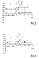
- Figure 3 illustrates the energy level in electron volts (eV) of the area around the active region 6 of a transferred electron effect device 1b which differs from the transferred electron effect device 1a of Figure 2 merely by virtue of the fact that the doping within the well region 10a has been increased to 5x10 18 atoms cm -3 , that is 2.5 times the doping of the well region of the transferred electron effect device of Figure 2.
- eV electron volts
- the solid 20b, dashed 21b and dotted 22b lines in Figure 3 correspond to the solid 20a, dashed 21a and dotted 22a lines of Figure 2.
- the Fermi level is now higher in the well region 10a so that there is no depletion of the active region 6; rather it is actually accumulating electrons.
- the energy difference E i has now dropped to 0.29eV. This suggests that the optimum doping concentration for the well region 10a is to be found between the doping concentrations of the examples of transferred electron effect devices 1a and 1b shown in Figures 2 and 3, that is between 2x10 18 atoms cm -3 and 5x10 18 atoms cm -3 .
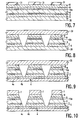
- Figure 4 shows a cross-section through part of a modified transferred electron effect device 1c while Figure 5 illustrates the energy level in electron volts (eV) across the transferred electron effect device 1c which differs from the transferred electron effect device 1a of Figure 2 in that the well region 10b is not directly doped but is doped by modulation-doping.
- the solid 20c, dashed 21c and dotted 22c lines in Figure 5 correspond to the solid 20a, dashed 21a and dotted 22a lines of Figure 2.
- the well region 10b is formed of intrinsic gallium indium arsenide with the same composition as given above.
- the well region 10b is spaced from the active region 6 by a spacer region 11.
- the spacer region 11 separates the well region from a doped modulation region 12.
- Both the spacer region 11 and the modulation region 12 are formed of indium phosphide.
- the various regions are formed of the same material and have the same dopings and thicknesses as in Figure 2, but, as indicated above, the well region is not intentionally doped and the indium phosphide spacer and modulation regions 11 and 12 have been added.
- the spacer and modulation regions 11 and 12 are both, in this example, 2nm thick and the modulation region 12 is doped with suitable n conductivity impurities to a dopant concentration of 5x10 18 atoms cm -3 .
- the spacer region 11 could be omitted, if desired.
- the use of a modulation doping arrangement enables the dopant to be separated from the well region 10b allowing the width of the well region 10b and the dopant concentration to be determined separately.
- the transferred electron effect device 1c illustrated by Figures 4 and 5 uses less dopant (1x10 12 cm -2 ) than the transferred electron effect devices 1a and 1b because the modulation region 12 is thinner than the well region 10a.
- the Fermi level is much lower than in the transferred electron effect devices 1a and 1b, thereby improving the injection energy E i to as high as 0.44eV. This makes it even more likely that electrons emitted over the barrier provided by the graded band gap injector will be transferred directly to a satellite conduction band minimum and so should provide an even better output power and efficiency than the example shown in Figure 2.
- Figure 5 does show a slight reduction in carrier density in the drift region 6 under the strong forward bias shown by line 21d, but reduction could be avoided by an appropriate increase in the dopant concentration within the modulation region 12 without affecting the position of the Fermi level in the well region 10b.
- Figure 6 illustrates schematically the energy level in electron volts (eV) across the area around the active region 6 of a transferred electron effect device 1d having the structure shown in Figure 1 and the same thicknesses and dopant concentrations as in the example described above with reference to Figure 2 but without the well region 10a.
- eV electron volts
- the well region 10a is replaced by a highly doped depletion stop region 100 of the same material as the active region 6, indium phosphide in these examples.
- the depletion stop 100 should, of course, be sufficiently thin to allow the passage of hot charge carriers, that is charge carriers with an energy above the Fermi level of the active region 6, to pass without significant cooling or thermalisation.
- the depletion stop 100 has the same thickness, 10nm, as the well region 10a, 10b and has a dopant concentration of 2x10 18 cm -3 .
- the solid line 20d in Figure 6 illustrates the conduction band energy when no voltages are applied to the cathode and anode electrodes 4 and 7 while the dashed line 21d illustrates the change in the conduction band energy level when a forward-biasing voltage of 30 volts is applied between the cathode and anode electrodes 4 and 7.
- the dotted line 22d represents the applied forward-biasing voltage Vf.
- the Fermi level is again defined as the zero level in Figure 6.
- the energy difference E i is merely 0.17eV because the indium phosphide depletion stop 10 acts to drag down the Fermi level adjacent the barrier.
- the transferred electron effect device 1a structure illustrated by Figure 6 probably would not allow electrons to be injected into the active region with sufficient energy to transfer directly to a satellite minimum and a significant proportion of the active region would be taken up in operation of the device 1d by the acceleration or dead zone required for electrons to gain sufficient energy to transfer to a conduction band satellite minimum.
- the device 1d will have a lower output power and efficiency than any of the devices 1a to 1c described above.
- the examples in accordance with the invention described above with reference to Figures 2 to 5 provide an energy difference E i that is much greater than that provided by the example shown in Figure 6. Indeed, an energy difference E i over twice the energy difference E i for the example of the transferred electron effect device 1d illustrated by Figure 6 is achieved by the example of a transferred electron effect device 1a shown in Figure 2 while an even energy difference is attained by the device 1c illustrated by Figures 4 and 5.
- the improved energy difference is achieved because, as can be seen by comparing Figures 2, 3 and 5 with Figure 6, the band bending which arises when the indium phosphide depletion stop 10 is used in the example shown in Figure 6 is avoided when a well region 10a, 10b in accordance with the invention is provided.
- the present inventor has thus found that replacing the indium phosphide depletion stop region 10 with a well region 10a or 10b causes a significant increase in the energy difference E i and enables electrons to be emitted over the barrier P provided by the graded band gap region 9 with an energy comparable to that of a conduction band satellite minimum, which electrons can thus transfer directly to a conduction band satellite minimum, without the need for any acceleration or dead zone, to enable the transferred electron effect device 1b to exhibit negative differential resistance. Accordingly, a device in accordance with the invention can exhibit higher rf output powers and greater efficiencies than a device such as that shown in Figure 6.
- FIGS. 7 to 10 illustrate one way of manufacturing a transferred electron effect device in accordance with the invention.
- the various semiconductor regions forming the device are epitaxially deposited onto a suitable monocrystalline semiconductor substrate 30 by any suitable technique such as molecular beam epitaxy (MBE) or metal organic vapour phase epitaxy (MOVPE) so that the anode contact region 5 is adjacent the substrate.
- Discrete transferred electron effect devices 1a are then defined by providing a photosensitive resist mask 31 on the exposed surface of the cathode contact region 8 and etching the regions using a suitable etching process to define the devices 1a as discrete mesas.
- the indium gallium arsenide anode contact region 5 is used as an etch stop layer so that the etching terminates at the substrate 30.
- a sacrificial support layer 32 of a suitable material is then provided on cathode contact regions 8 as shown in Figure 8.
- the support layer 32 may be formed by plating a metal such as silver normally used for heat sinks.
- the substrate 30 is then selectively removed by a suitable etching process and a suitable metal deposited onto the exposed surfaces of the anode contact regions to form the anode electrode and heat sink.
- the anode electrode 4 may comprise two subsidiary layers one of which 4a functions to provide the ohmic contract to the anode contact region 9 and the other 4b of which functions primarily as a heat sink. Again the heat sink may be formed of silver.
- the sacrificial support layer 32 is then removed and metal deposited to form the cathode electrodes 7 as shown in Figure 10.
- This method is advantageous in that the active region 6 is grown before the injector region 9 so that the injector region 9 is not subjected to the prolonged high temperature processing required to form the active region 6. Also, as indicated in our US Patent No. 5, 250,815, the provision of the heat sink at the anode rather than the cathode of a transferred electron effect device having an injector region results in surprising improvements in, especially, rf output power.
- the present invention could be applied where other materials are used, for example where the active region is formed of gallium arsenide or of materials containing indium phosphide or gallium arsenide.
- the active region is formed of gallium arsenide or of materials containing indium phosphide or gallium arsenide.
- appropriate changes would have to be made to the other III-V materials used to form the device.
- the present invention may also be applied to devices with different types of injector regions, for example injector regions of the type described and claimed in our US Patent No. 5,258,624.
- the provision of the highly doped gallium indium arsenide anode and cathode contact regions 5 and 8 allows the anode and cathode electrodes 4 and 7 to make good ohmic contact to the transferred electron effect device structure without having to resort to the out-diffusion of dopants from the electrodes 4 and 7.
- the highly doped gallium indium arsenide anode and cathode contact regions 5 and 8 will be lattice-matched to the adjoining regions and in the examples described above have the composition Ga 0.47 In 0.53 As so as to provide a lattice match between the contact region 8 and the graded band gap injector region 9.
- highly doped gallium indium arsenide contact regions may be used anywhere it is desired to form an ohmic contact to an indium phosphide region or device.
Landscapes
- Electrodes Of Semiconductors (AREA)
- Junction Field-Effect Transistors (AREA)
- Recrystallisation Techniques (AREA)
Claims (11)
- Elektronentransfereffektanordnung mit einem Halbleiterkörper, welcher eine aktive Zone (6) des n-Leitfähigkeitstyps, die aus einem Material besteht, welches ein, eine relativ geringe Masse und hohe Mobilität vorsehendes Zentralminimum des Leitungsbandes und zumindest ein, eine relativ hohe Masse und geringe Mobilität vorsehendes Satellitenminimum des Leitungsbandes aufweist, sowie eine Injektionszone (9) vorsieht, welche eine Potentialbarriere für den Fluß der Elektronen in die aktive Zone in einem Umfang definiert, daß Elektronen mit einer zur Überwindung der durch die Injektionszone (9) vorgesehenen Barriere ausreichenden Energie bei Betrieb der Anordnung mit einer Energie, welche mit dieser des mindestens einen, eine relativ hohe Masse und geringe Mobilität aufweisenden Satellitenminimums des Leitungsbandes vergleichbar ist, in die aktive Zone (6) emittiert werden, dadurch gekennzeichnet, daß eine, Elektronen enthaltende Wannenzone (10a) aus einem anderen Material als diesem der aktiven Zone und der Injektionszone zwischen der Injektionszone und der aktiven Zone vorgesehen ist, um die Ausbreitung eines Verarmungsgebietes in die aktive Zone bei Betrieb der Anordnung zu unterbinden.
- Elektronentransfereffektanordnung nach Anspruch 1, wobei die Injektionszone eine abgestufte Bandabstandsinjektionszone aufweist.
- Elektronentransfereffektanordnung nach Anspruch 2, wobei die aktive Zone Indiumphosphid und die abgestufte Bandabstandsinjektionszone Galliumaluminiumindiumphosphid aufweist.
- Elektronentransfereffektanordnung nach Anspruch 3, wobei die abgestufte Bandabstandsinjektionszone Ga0.48xAl0.48(1-x)In0.52As aufweist, wobei x von 1 zu 0 hin in Richtung der aktiven Zone abnimmt.
- Elektronentransfereffektanordnung nach Anspruch 3 oder 4, wobei die Wannenzone Galliumindiumarsenid vom n-Leitfähigkeitstyp aufweist.
- Elektronentransfereffektanordnung nach einem der Ansprüche 1 bis 4, wobei die Wannenzone nicht vorsätzlich dotiert wird und eine relativ stark dotierte Halbleitermodulationszone so dotiert wird, daß sie n-leitend ist und die Wannenzone von der aktiven Zone trennt.
- Elektronentransfereffektanordnung nach Anspruch 6, wobei die Modulationszone von der Wannenzone durch eine, aus dem gleichen Halbleiter wie die Modulationszone gebildete, eigenleitende Abstandszone getrennt ist.
- Elektronentransfereffektanordnung nach Anspruch 6 oder 7, wobei die Wannenzone Galliumindiumarsenid und die Modulationszone Indiumphosphid aufweist.
- Elektronentransfereffektanordnung nach einem der vorangegangenen Ansprüche, wobei die aktive Zone zur n-Leitung dotiertes Indiumphosphid aufweist, die Anoden- und Kathodenhalbleiterzone durch die aktive Zone voneinander beabstandet sind und jeweils zur n-Leitung stark dotierte Halbleiterzonen sowie eine die Anoden- und Kathodenzone jeweils kontaktierende Anoden- und Kathodenelektrode aufweisen, wobei die Kathodenhalbleiterzone die Injektionszone (9) und die Elektronen enthaltende Wannenzone (10a) aufweist und die Anoden- und Kathodenzone stark dotierte, n-leitende Galliumindiumarsenidzonen aufweisen, welche mit der Anoden- und der Kathodenelektrode jeweils einen ohmschen Kontakt herstellen.
- Elektronentransfereffektanordnung nach einem der vorangegangenen Ansprüche und mit einer Anoden- und Kathodenhalbleiterzone, welche durch die aktive Zone (6) beabstandet sind, wobei die Kathodenhalbleiterzone die Injektionszone (9) und die Elektronen enthaltende Wannenzone (10a) aufweist und wobei eine Wärmeableitungszone auf der freigelegten Oberfläche der Anodenzone vorgesehen ist, um in der Anordnung abgeleitete Wärme abzuführen.
- Verfahren zur Herstellung einer Elektronentransfereffektanordnung nach Anspruch 10, wonach ein Halbleitersubstrat und auf dem Substrat eine Epitaxieschichtstruktur vorgesehen wird, um den Halbleiterkörper mit der, auf dem Substrat ausgebildeten Anodenzone sowie der aktiven und der Kathodenzone zu definieren, dadurch gekennzeichnet, daß nach Definieren des Halbleiterkörpers das Substrat selektiv entfernt wird, um eine Oberfläche der Anodenzone freizulegen und sodann auf der freigelegten Oberfläche der Anodenzone eine Wärmeableitungszone vorgesehen wird, um in der Epitaxieschichtstruktur abgeleitete Wärme abzuführen.
Applications Claiming Priority (3)
| Application Number | Priority Date | Filing Date | Title |
|---|---|---|---|
| GB9414311A GB9414311D0 (en) | 1994-07-15 | 1994-07-15 | A transferred electron effect device |
| GB9414311 | 1994-07-15 | ||
| PCT/IB1995/000550 WO1996002964A2 (en) | 1994-07-15 | 1995-07-10 | A transferred electron effect device |
Publications (2)
| Publication Number | Publication Date |
|---|---|
| EP0720779A1 EP0720779A1 (de) | 1996-07-10 |
| EP0720779B1 true EP0720779B1 (de) | 1999-12-29 |
Family
ID=10758393
Family Applications (1)
| Application Number | Title | Priority Date | Filing Date |
|---|---|---|---|
| EP95922698A Expired - Lifetime EP0720779B1 (de) | 1994-07-15 | 1995-07-10 | Elektronentransfereffektanordnung |
Country Status (6)
| Country | Link |
|---|---|
| US (1) | US5675157A (de) |
| EP (1) | EP0720779B1 (de) |
| JP (1) | JPH09507967A (de) |
| DE (1) | DE69514204T2 (de) |
| GB (1) | GB9414311D0 (de) |
| WO (1) | WO1996002964A2 (de) |
Families Citing this family (11)
| Publication number | Priority date | Publication date | Assignee | Title |
|---|---|---|---|---|
| US6303940B1 (en) * | 1999-01-26 | 2001-10-16 | Agere Systems Guardian Corp. | Charge injection transistor using high-k dielectric barrier layer |
| US6596617B1 (en) | 2000-06-22 | 2003-07-22 | Progressant Technologies, Inc. | CMOS compatible process for making a tunable negative differential resistance (NDR) device |
| US6518589B2 (en) * | 2000-06-22 | 2003-02-11 | Progressant Technologies, Inc. | Dual mode FET & logic circuit having negative differential resistance mode |
| US6559470B2 (en) * | 2000-06-22 | 2003-05-06 | Progressed Technologies, Inc. | Negative differential resistance field effect transistor (NDR-FET) and circuits using the same |
| US6956262B1 (en) | 2001-12-21 | 2005-10-18 | Synopsys Inc. | Charge trapping pull up element |
| US7453083B2 (en) * | 2001-12-21 | 2008-11-18 | Synopsys, Inc. | Negative differential resistance field effect transistor for implementing a pull up element in a memory cell |
| DE10261238A1 (de) * | 2002-12-20 | 2004-07-15 | Forschungszentrum Jülich GmbH | Schichtenfolge |
| DE102004044558A1 (de) * | 2004-09-15 | 2006-04-06 | Forschungszentrum Jülich GmbH | Gunn-Diode |
| GB0608515D0 (en) * | 2006-04-28 | 2006-06-07 | Univ Aberdeen | Semiconductor device for generating an oscillating voltage |
| DE102007007159B4 (de) * | 2007-02-09 | 2009-09-03 | Technische Universität Darmstadt | Gunn-Diode |
| US8981312B1 (en) * | 2013-09-10 | 2015-03-17 | Sandia Corporation | Photon detector configured to employ the Gunn effect and method of use |
Family Cites Families (14)
| Publication number | Priority date | Publication date | Assignee | Title |
|---|---|---|---|---|
| GB1286674A (en) * | 1969-06-10 | 1972-08-23 | Secr Defence | Transferred electron devices |
| US3755752A (en) * | 1971-04-26 | 1973-08-28 | Raytheon Co | Back-to-back semiconductor high frequency device |
| US3753804A (en) * | 1971-08-31 | 1973-08-21 | Philips Corp | Method of manufacturing a semiconductor device |
| US3789322A (en) * | 1972-11-24 | 1974-01-29 | United Aircraft Corp | Microwave cavity tuning loop including a varactor |
| US4238763A (en) * | 1977-08-10 | 1980-12-09 | National Research Development Corporation | Solid state microwave devices with small active contact and large passive contact |
| JPS5477064A (en) * | 1977-12-02 | 1979-06-20 | Nippon Telegr & Teleph Corp <Ntt> | Electrode forming method of compound semiconductors |
| US4257055A (en) * | 1979-07-26 | 1981-03-17 | University Of Illinois Foundation | Negative resistance heterojunction devices |
| US4539581A (en) * | 1982-07-12 | 1985-09-03 | The United States Of America As Represented By The Secretary Of The Army | Planar doped barrier transferred electron oscillator |
| US4649405A (en) * | 1984-04-10 | 1987-03-10 | Cornell Research Foundation, Inc. | Electron ballistic injection and extraction for very high efficiency, high frequency transferred electron devices |
| US4851886A (en) * | 1986-06-11 | 1989-07-25 | Texas Instruments Incorporated | Binary superlattice tunneling device and method |
| GB8623208D0 (en) * | 1986-09-26 | 1986-10-29 | Gen Electric Co Plc | Electronic devices |
| US5258624A (en) * | 1988-05-27 | 1993-11-02 | U.S. Philips Corp. | Transferred electron effect device |
| GB2245421A (en) * | 1990-06-20 | 1992-01-02 | Philips Electronic Associated | Gunn effect device having a heat sink |
| JPH0738175A (ja) * | 1993-07-22 | 1995-02-07 | Showa Denko Kk | ガンダイオード |
-
1994
- 1994-07-15 GB GB9414311A patent/GB9414311D0/en active Pending
-
1995
- 1995-07-10 WO PCT/IB1995/000550 patent/WO1996002964A2/en not_active Ceased
- 1995-07-10 DE DE69514204T patent/DE69514204T2/de not_active Expired - Fee Related
- 1995-07-10 EP EP95922698A patent/EP0720779B1/de not_active Expired - Lifetime
- 1995-07-10 JP JP8504852A patent/JPH09507967A/ja not_active Ceased
- 1995-07-13 US US08/501,893 patent/US5675157A/en not_active Expired - Fee Related
Also Published As
| Publication number | Publication date |
|---|---|
| WO1996002964A3 (en) | 1996-12-19 |
| JPH09507967A (ja) | 1997-08-12 |
| DE69514204T2 (de) | 2000-08-24 |
| US5675157A (en) | 1997-10-07 |
| EP0720779A1 (de) | 1996-07-10 |
| WO1996002964A2 (en) | 1996-02-01 |
| DE69514204D1 (de) | 2000-02-03 |
| GB9414311D0 (en) | 1994-09-07 |
Similar Documents
| Publication | Publication Date | Title |
|---|---|---|
| US4683484A (en) | Lateral confinement of charge carriers in a multiple quantum well structure | |
| US5789768A (en) | Light emitting diode having transparent conductive oxide formed on the contact layer | |
| KR0153781B1 (ko) | 헤테로 접합 밴드 불연속의 제거 디바이스 및 그 방법 | |
| US5504347A (en) | Lateral resonant tunneling device having gate electrode aligned with tunneling barriers | |
| US5495115A (en) | Semiconductor crystalline laminate structure, forming method of the same, and semiconductor device employing the same | |
| US7719028B2 (en) | Semiconductor light-receiving device and manufacturing method thereof | |
| US20050029541A1 (en) | Charge controlled avalanche photodiode and method of making the same | |
| US20100213513A1 (en) | Hyperabrupt Diode Structure And Method For Making Same | |
| EP0199435B1 (de) | Feldeffekt-Halbleiteranordnung | |
| US8124957B2 (en) | Low resistance tunnel junctions in wide band gap materials and method of making same | |
| US6670653B1 (en) | InP collector InGaAsSb base DHBT device and method of forming same | |
| US5675157A (en) | Transferred electron effect device | |
| US5949096A (en) | Field effect transistor with stabilized threshold voltage | |
| JP2760596B2 (ja) | 導波路構造を有する半導体デバイスおよびその製造方法 | |
| EP0314372A2 (de) | Stromeingrenzungs- und Blockierungsgebiet für Halbleitervorrichtungen | |
| US5548139A (en) | Schottky gate field effect transistor | |
| US6057566A (en) | Semiconductor device | |
| EP0200422B1 (de) | Transistoranordnung | |
| US4905057A (en) | Semiconductor devices | |
| CN112531051A (zh) | 一种隧道结结构及其形成方法、隧道结器件 | |
| JPH02121382A (ja) | 埋込みストライプ半導体レーザーの製造方法及びその半導体レーザー | |
| JPH0658972B2 (ja) | ラテラルp−i−nヘテロ接合デバイス及びその形成方法 | |
| US6242765B1 (en) | Field effect transistor and its manufacturing method | |
| EP1008187A2 (de) | Halbleiter mit gleichrichtendem übergang und seine herstellung | |
| EP0361759A2 (de) | Heterostrukturbipolartransistor |
Legal Events
| Date | Code | Title | Description |
|---|---|---|---|
| PUAI | Public reference made under article 153(3) epc to a published international application that has entered the european phase |
Free format text: ORIGINAL CODE: 0009012 |
|
| AK | Designated contracting states |
Kind code of ref document: A1 Designated state(s): DE FR GB IT |
|
| 17P | Request for examination filed |
Effective date: 19960801 |
|
| PUAK | Availability of information related to the publication of the international search report |
Free format text: ORIGINAL CODE: 0009015 |
|
| D17P | Request for examination filed (deleted) | ||
| R17P | Request for examination filed (corrected) |
Effective date: 19970619 |
|
| 17Q | First examination report despatched |
Effective date: 19980311 |
|
| RAP3 | Party data changed (applicant data changed or rights of an application transferred) |
Owner name: PHILIPS ELECTRONICS UK LIMITED Owner name: KONINKLIJKE PHILIPS ELECTRONICS N.V. |
|
| GRAG | Despatch of communication of intention to grant |
Free format text: ORIGINAL CODE: EPIDOS AGRA |
|
| GRAG | Despatch of communication of intention to grant |
Free format text: ORIGINAL CODE: EPIDOS AGRA |
|
| GRAH | Despatch of communication of intention to grant a patent |
Free format text: ORIGINAL CODE: EPIDOS IGRA |
|
| GRAH | Despatch of communication of intention to grant a patent |
Free format text: ORIGINAL CODE: EPIDOS IGRA |
|
| GRAA | (expected) grant |
Free format text: ORIGINAL CODE: 0009210 |
|
| AK | Designated contracting states |
Kind code of ref document: B1 Designated state(s): DE FR GB IT |
|
| PG25 | Lapsed in a contracting state [announced via postgrant information from national office to epo] |
Ref country code: IT Free format text: LAPSE BECAUSE OF FAILURE TO SUBMIT A TRANSLATION OF THE DESCRIPTION OR TO PAY THE FEE WITHIN THE PRESCRIBED TIME-LIMIT;WARNING: LAPSES OF ITALIAN PATENTS WITH EFFECTIVE DATE BEFORE 2007 MAY HAVE OCCURRED AT ANY TIME BEFORE 2007. THE CORRECT EFFECTIVE DATE MAY BE DIFFERENT FROM THE ONE RECORDED. Effective date: 19991229 |
|
| REF | Corresponds to: |
Ref document number: 69514204 Country of ref document: DE Date of ref document: 20000203 |
|
| ET | Fr: translation filed | ||
| PLBE | No opposition filed within time limit |
Free format text: ORIGINAL CODE: 0009261 |
|
| STAA | Information on the status of an ep patent application or granted ep patent |
Free format text: STATUS: NO OPPOSITION FILED WITHIN TIME LIMIT |
|
| 26N | No opposition filed | ||
| REG | Reference to a national code |
Ref country code: GB Ref legal event code: IF02 |
|
| REG | Reference to a national code |
Ref country code: FR Ref legal event code: D6 |
|
| REG | Reference to a national code |
Ref country code: GB Ref legal event code: 746 Effective date: 20021205 |
|
| PGFP | Annual fee paid to national office [announced via postgrant information from national office to epo] |
Ref country code: DE Payment date: 20070919 Year of fee payment: 13 |
|
| PGFP | Annual fee paid to national office [announced via postgrant information from national office to epo] |
Ref country code: GB Payment date: 20070905 Year of fee payment: 13 |
|
| PGFP | Annual fee paid to national office [announced via postgrant information from national office to epo] |
Ref country code: FR Payment date: 20070725 Year of fee payment: 13 |
|
| GBPC | Gb: european patent ceased through non-payment of renewal fee |
Effective date: 20080710 |
|
| PG25 | Lapsed in a contracting state [announced via postgrant information from national office to epo] |
Ref country code: DE Free format text: LAPSE BECAUSE OF NON-PAYMENT OF DUE FEES Effective date: 20090203 |
|
| REG | Reference to a national code |
Ref country code: FR Ref legal event code: ST Effective date: 20090331 |
|
| PG25 | Lapsed in a contracting state [announced via postgrant information from national office to epo] |
Ref country code: GB Free format text: LAPSE BECAUSE OF NON-PAYMENT OF DUE FEES Effective date: 20080710 |
|
| PG25 | Lapsed in a contracting state [announced via postgrant information from national office to epo] |
Ref country code: FR Free format text: LAPSE BECAUSE OF NON-PAYMENT OF DUE FEES Effective date: 20080731 |