EP0723245A2 - Halbzeug mit einem elektronischen Modul - Google Patents
Halbzeug mit einem elektronischen Modul Download PDFInfo
- Publication number
- EP0723245A2 EP0723245A2 EP95120312A EP95120312A EP0723245A2 EP 0723245 A2 EP0723245 A2 EP 0723245A2 EP 95120312 A EP95120312 A EP 95120312A EP 95120312 A EP95120312 A EP 95120312A EP 0723245 A2 EP0723245 A2 EP 0723245A2
- Authority
- EP
- European Patent Office
- Prior art keywords
- integrated circuit
- semi
- carrier layers
- electronic module
- cavity
- Prior art date
- Legal status (The legal status is an assumption and is not a legal conclusion. Google has not performed a legal analysis and makes no representation as to the accuracy of the status listed.)
- Granted
Links
Images

Classifications
-
- G—PHYSICS
- G06—COMPUTING OR CALCULATING; COUNTING
- G06K—GRAPHICAL DATA READING; PRESENTATION OF DATA; RECORD CARRIERS; HANDLING RECORD CARRIERS
- G06K19/00—Record carriers for use with machines and with at least a part designed to carry digital markings
- G06K19/06—Record carriers for use with machines and with at least a part designed to carry digital markings characterised by the kind of the digital marking, e.g. shape, nature, code
- G06K19/067—Record carriers with conductive marks, printed circuits or semiconductor circuit elements, e.g. credit or identity cards also with resonating or responding marks without active components
- G06K19/07—Record carriers with conductive marks, printed circuits or semiconductor circuit elements, e.g. credit or identity cards also with resonating or responding marks without active components with integrated circuit chips
- G06K19/077—Constructional details, e.g. mounting of circuits in the carrier
- G06K19/07749—Constructional details, e.g. mounting of circuits in the carrier the record carrier being capable of non-contact communication, e.g. constructional details of the antenna of a non-contact smart card
- G06K19/07773—Antenna details
- G06K19/07777—Antenna details the antenna being of the inductive type
- G06K19/07779—Antenna details the antenna being of the inductive type the inductive antenna being a coil
-
- G—PHYSICS
- G06—COMPUTING OR CALCULATING; COUNTING
- G06K—GRAPHICAL DATA READING; PRESENTATION OF DATA; RECORD CARRIERS; HANDLING RECORD CARRIERS
- G06K19/00—Record carriers for use with machines and with at least a part designed to carry digital markings
- G06K19/06—Record carriers for use with machines and with at least a part designed to carry digital markings characterised by the kind of the digital marking, e.g. shape, nature, code
- G06K19/067—Record carriers with conductive marks, printed circuits or semiconductor circuit elements, e.g. credit or identity cards also with resonating or responding marks without active components
- G06K19/07—Record carriers with conductive marks, printed circuits or semiconductor circuit elements, e.g. credit or identity cards also with resonating or responding marks without active components with integrated circuit chips
- G06K19/077—Constructional details, e.g. mounting of circuits in the carrier
- G06K19/07749—Constructional details, e.g. mounting of circuits in the carrier the record carrier being capable of non-contact communication, e.g. constructional details of the antenna of a non-contact smart card
-
- G—PHYSICS
- G06—COMPUTING OR CALCULATING; COUNTING
- G06K—GRAPHICAL DATA READING; PRESENTATION OF DATA; RECORD CARRIERS; HANDLING RECORD CARRIERS
- G06K19/00—Record carriers for use with machines and with at least a part designed to carry digital markings
- G06K19/06—Record carriers for use with machines and with at least a part designed to carry digital markings characterised by the kind of the digital marking, e.g. shape, nature, code
- G06K19/067—Record carriers with conductive marks, printed circuits or semiconductor circuit elements, e.g. credit or identity cards also with resonating or responding marks without active components
- G06K19/07—Record carriers with conductive marks, printed circuits or semiconductor circuit elements, e.g. credit or identity cards also with resonating or responding marks without active components with integrated circuit chips
- G06K19/077—Constructional details, e.g. mounting of circuits in the carrier
- G06K19/07749—Constructional details, e.g. mounting of circuits in the carrier the record carrier being capable of non-contact communication, e.g. constructional details of the antenna of a non-contact smart card
- G06K19/07773—Antenna details
- G06K19/07777—Antenna details the antenna being of the inductive type
- G06K19/07779—Antenna details the antenna being of the inductive type the inductive antenna being a coil
- G06K19/07781—Antenna details the antenna being of the inductive type the inductive antenna being a coil the coil being fabricated in a winding process
Definitions
- the invention relates to a semi-finished product, suitable for installation in a data carrier, with an electronic module, comprising at least one integrated circuit and a coil conductively connected to the circuit, the coil being arranged between two carrier layers and the integrated circuit in a cavity provided for this purpose is arranged both carrier layers.
- Semi-finished products of the type mentioned have been known for a long time. They are used to manufacture data media from this, which are used, for example, in the internal area as access authorization.
- the power supply of the electronic module and / or the data exchange with external devices is not touching the coil.
- Such a semi-finished product with an electronic module is known for example from WO 92/21105.
- the semi-finished product consists of two card layers laminated on top of each other. One of the layers has suitable depressions in the form of blind holes for receiving the integrated circuit and the coil conductively connected to the circuit, the second layer closing the depressions with the integrated circuit and the coil arranged therein.
- the data carrier is finished from the semi-finished product by laminating cover layers onto the semi-finished product on both sides.
- an integrated circuit is located in a cavity of the card layers. Since the integrated circuit does not completely fill the cavity in question, an undesired deformation of the cover layers in the area of the cavity often occurs in the finished data carrier.
- the invention is therefore based on the object of presenting a semi-finished product for producing a data carrier, with which data carriers with completely flat cover layers can be achieved.
- the basic idea of the invention is to be seen in the fact that the remaining cavity between the carrier layers and the integrated circuit is filled with a filler material in such a way that flat surfaces of the semi-finished product result in the region of the cavity, which are flush with the surfaces of the carrier layers.
- the electronic module is embedded between two carrier layers.
- the semi-finished product is suitable for the production of data carriers with very flat surfaces, which can be produced by laminating top layers onto the semi-finished product.
- the coil is located in the semifinished product between the carrier layers, while the integrated circuit is arranged in a cavity of the two carrier layers provided for this purpose.
- the remaining cavity between the integrated circuit and the layers is filled with a filling material so that the semi-finished product has completely flat surfaces.
- the carrier layers preferably have the same thickness.
- depressions can be formed in the carrier layers, which form a channel that at least partially receives the coil.
- the channel can be partially filled with filler material.
- an electronic module for the contacting data exchange can also be provided, comprising at least contact areas and a conductor with the contact areas connected integrated circuit, be accommodated in a further cavity of the carrier layers.
- the remaining cavity between the module and the carrier layers is also filled with a filling material.
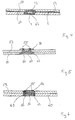
- FIGS. 1-6 show a semi-finished product according to the invention in cross section, which has a cavity in one area. All of the exemplary embodiments have in common that the cavity is filled with a filling compound in such a way that the semifinished product has flat surfaces.
- the semifinished products shown in FIGS. 1-6 can thus be provided with cover layers without these noticeably deforming in the region of the cavity.
- This has the advantage that the cover layers can be provided in whole or in part with an element which, for certain reasons, requires a flat surface.
- Such an element can e.g. B. be a hologram whose optical effect is based on fine structures that can be disturbed by a non-flat surface.
- Another such element is a magnetic stripe, the data of which can only be reliably read out with a reading head if the stripe lies on a surface that is as flat as possible.
- Other elements are conceivable.
- Fig. 1 shows the semi-finished product in a filling station.
- the semifinished product comprises the carrier layers 38 and 39, between which the coil 2 is located.
- the ends of the coil 2 are conductively connected to a chip carrier 61, in the interior of which the integrated circuit 4, not shown here, is located.
- the chip carrier 61 is arranged in an opening in the carrier layers 38 and 39.
- the remaining cavity is filled with a filling compound 42 such that even in the area of the opening there are flat surfaces which are flush with the outer surfaces of the layers 38 and 39, as shown in the figure.
- a wide variety of materials can be used as the filler 42, such as casting resins that cure under heat and UV light or thermoplastic materials etc.
- a semi-finished product just described is produced as follows.
- the electronic module consisting of the coil 2 and the chip carrier 61 conductively connected to the ends of the coil, is placed on the layer 39, so that the chip carrier 61 is arranged in the opening in the layer 39 provided for this purpose.
- the opening can be punched, for example.
- the layer 38 is then laminated onto the layer 39. This can happen, for example, under the influence of heat and pressure.
- the layers can also be laminated to one another by the ultrasound welding method already well known to the person skilled in the art. This has the advantage that the coils act as energy direction transmitters, as a result of which the carrier layers weld particularly well and no more voids remain between the coil wires.
- the laminate is placed between the filling station halves 40 and 41 (cf. is injected into the remaining cavity through the sprue 43. This can preferably be done under increased pressure, which ensures that the entire remaining cavity is filled with filling compound.
- the filling station can additionally be used to connect the carrier layers 38 and 39 to one another, e.g. B. under the influence of heat and pressure. In this case, at least one of the filling station halves can be heated.
- the filling station halves are preferably made of metal, but can also be adapted to the respective filling material 42 and z. B. consist of a UV-transparent material when UV-curing potting compound is used.
- filling stations can also be arranged next to one another and the layers 38 and 39 described are present in the form of long strips which are cut to length shortly before the data medium is finished.
- Fig. 2 shows a first development of the semi-finished product in cross section.
- the electronic module in this case comprises the coil 2 and the integrated circuit 4 connected directly to it.
- the carrier layers 44 and 45 have, in addition to the openings for the integrated circuit 4, additional depressions 46 which form a channel for a portion of the coil and can, for example, in Injection molding can be made.
- the depressions serve to hold excess filling material 42.
- the semi-finished product is produced analogously to the above-mentioned method.
- Fig. 3 shows a second development of the semi-finished product in cross section.
- the semifinished product essentially corresponds to that in FIG. 2.
- the depressions 47 forming the channel for the coil are formed for the entire coil 2, so that the entire coil runs in one channel.
- the remaining cavity in the depressions 47 is at least partially filled with the filling material 42.
- the layer 48 has no opening to accommodate the integrated circuit.
- the semi-finished product is also produced essentially analogously to the method described in connection with FIG. 1. However, the filler material 42 is injected from below.
- FIG. 4 shows a third development of the semi-finished product in cross section, which essentially corresponds to that of FIG. 3.
- an indentation for receiving the integrated circuit 4 is provided in the upper carrier layer 50.
- the lower carrier layer 51 has a recess for receiving the integrated circuit 4 and an opening 62 for filling the filler material 42. The production takes place analogously to the method described in connection with FIG. 3.
- Fig. 5 shows a fourth development of the semi-finished product in cross section.
- a second electronic module for the contacting data exchange is arranged in a further opening in the carrier layers.
- the electronic module consists of an integrated circuit 57 which is fastened on a carrier substrate 56 and is conductively connected through openings in the carrier substrate 56 via bonding wires 64 to contact areas 55 which are on the side of the carrier substrate opposite the circuit 57.
- the installation takes place z. B. after installing the non-contacting electronic module.
- the carrier substrate 56 is connected to the card layer 53 such that the integrated circuit 57 and the conductive connections 64 lie in the openings of the layers 53 and 54 provided for this purpose, as is also shown in FIG. 5.
- the remaining cavity in the openings in the card layers 53 and 54 is then filled with a filler 42 from the side facing away from the electronic module by the method described above.
- This will electronic module fixed in the opening of the card layers 53 and 54.
- a particularly good fixation of the electronic module is achieved when the opening in the layer 54 is larger than the opening in the layer 53.
- the layer 53 is surrounded by the carrier substrate 56 on the one hand and by the filling compound 42 on the other hand, such as it is also shown in FIG. 5, so that the electronic module is well secured against forces acting perpendicular to the layers 53 and 54, respectively.
- FIG. 6 shows a fifth development of a semifinished product according to the invention.
- an electronic module is also used for the contact-making removal in an opening in the carrier layers 59 and 60.
- the electronic module for the contact removal is essentially constructed like that shown in FIG. 5.
- the integrated circuit is surrounded by a casting compound 58, which can consist of materials which are already well known to the person skilled in the art.
- the potting compound has a groove 63, so that the electronic module for the contact removal is better fixed in the opening in the carrier layers.
- the data carrier can be completed by covering layers being laminated on both sides of the semi-finished product. 5 or 6 in the semifinished products, the corresponding cover film has an opening in the area of the carrier substrate 56. The thickness of the top cover film should then be selected so that it is flush with the surface of the carrier substrate 56.
Landscapes
- Engineering & Computer Science (AREA)
- Computer Hardware Design (AREA)
- Microelectronics & Electronic Packaging (AREA)
- Physics & Mathematics (AREA)
- General Physics & Mathematics (AREA)
- Theoretical Computer Science (AREA)
- Computer Networks & Wireless Communication (AREA)
- Credit Cards Or The Like (AREA)
- Encapsulation Of And Coatings For Semiconductor Or Solid State Devices (AREA)
- Apparatuses And Processes For Manufacturing Resistors (AREA)
Abstract
Description
- Die Erfindung betrifft ein Halbzeug, geeignet zum Einbau in einen Datenträger, mit einem elektronischen Modul, umfassend zumindest einen integrierten Schaltkreis und eine leitend mit dem Schaltkreis verbundene Spule, wobei die Spule zwischen zwei Trägerschichten angeordnet ist und der integrierte Schaltkreis in einem dafür vorgesehenen Hohlraum der beiden Trägerschichten angeordnet ist.
- Halbzeuge der eingangs genannten Art sind bereits seit längerem bekannt. Sie werden verwendet, um hieraus Datenträger zu fertigen, die beispielsweise im innerbetrieblichen Bereich als Zugangsberechtigung verwendet werden. Die Energieversorgung des elektronischen Moduls und/oder der Datenaustausch mit externen Geräten erfolgt hierbei nichtberührend über die Spule.
- Ein derartiges Halbzeug mit elektronischem Modul ist beispielsweise aus der WO 92/21105 bekannt. Das Halbzeug besteht aus zwei übereinander laminierten Kartenschichten. Eine der Schichten hat hierbei geeignete Vertiefungen in Form von Sacklöchern zur Aufnahme des integrierten Schaltkreises und der mit dem Schaltkreis leitend verbundenen Spule, wobei die zweite Schicht die Vertiefungen mit dem darin angeordneten integrierten Schaltkreis und der Spule verschließt. Der Datenträger wird aus dem Halbzeug fertiggestellt, indem beidseitig Deckschichten auf das Halbzeug auflaminiert werden.
- In dem gezeigten Halbzeug befindet sich ein integrierter Schaltkreis in einem Hohlraum der Kartenschichten. Da der integrierte Schaltkreis den betreffenden Hohlraum nicht vollständig ausfüllt, kommt es beim fertiggestellten Datenträger oftmals zu einer unerwünschten Verformung der Deckschichten im Bereich des Hohlraums.
- Ausgehend von dem genannten Stand der Technik liegt der Erfindung deshalb die Aufgabe zugrunde, ein Halbzeug zur Herstellung eines Datenträgers vorzustellen, mit dem Datenträger mit vollkommen ebenen Deckschichten erzielt werden können.
- Die Aufgabe wird durch die in Anspruch 1 angegebenen Merkmale gelöst.
- Der Grundgedanke der Erfindung ist darin zu sehen, daß der verbleibende Hohlraum zwischen den Trägerschichten und dem integrierten Schaltkreis mit einem Füllmaterial derart aufgefüllt ist, daß sich hierdurch im Bereich des Hohlraums plane Oberflächen des Halbzeuges ergeben, die mit den Oberflächen der Trägerschichten fluchten.
- In einer Ausführungsform des Halbzeuges ist das elektronische Modul zwischen zwei Trägerschichten eingebettet. Das Halbzeug eignet sich zur Herstellung von Datenträgern mit sehr ebenen Oberflächen, die durch das Auflaminieren von Deckschichten auf das Halbzeug hergestellt werden können. Die Spule befindet sich in besagtem Halbzeug hierzu zwischen den Trägerschichten, während der integrierte Schaltkreis in einem dafür vorgesehenen Hohlraum der beiden Trägerschichten angeordnet ist. Der verbleibende Hohlraum zwischen dem integrierten Schaltkreis und den Schichten ist mit einem Füllmaterial aufgefüllt, so daß das Halbzeug vollkommen ebene Oberflächen aufweist. Vorzugsweise weisen die Trägerschichten dieselbe Dicke auf. Zusätzlich können in den Trägerschichten Vertiefungen ausgeformt sein, die einen Kanal bilden, der die Spule zumindest teilweise aufnimmt. Der Kanal kann teilweise mit Füllmaterial aufgefüllt sein.
- Neben dem elektronischen Modul für den nichtberührenden Datenaustausch kann zusätzlich ein elektronisches Modul für den berührenden Datenaustausch, umfassend zumindest Kontaktflächen und einem leitend mit den Kontaktflächen verbundenen integrierten Schaltkreis, in einem weiteren Hohlraum der Trägerschichten untergebracht sein. Der verbleibende Hohlraum zwischen dem Modul und den Trägerschichten ist hierbei gleichfalls mit einem Füllmaterial aufgefüllt.
- Weitere Vorteile und Weiterbildungen ergeben sich aus der Beschreibung, den Unteransprüchen sowie aus den Figuren, die nachfolgend erläutert werden.
- Darin zeigen:
- Fig. 1 - 6
- jeweils eine Schnittdarstellung durch ein Halbzeug, bei dem die Spule zwischen zwei Trägerschichten fixiert ist.
- Die Fig. 1 - 6 zeigen ein erfindungsgemäßes Halbzeug im Querschnitt, das in einem Bereich einen Hohlraum aufweist. Allen Ausführungsbeispielen ist gemeinsam, daß der Hohlraum derart mit einer Füllmasse aufgefüllt wird, daß das Halbzeug ebene Oberflächen aufweist. Die in den Fig. 1 - 6 gezeigten Halbzeuge können also mit Deckschichten versehen werden, ohne daß sich diese im Bereich des Hohlraums merklich verformen. Dies hat den Vorteil, daß die Deckschichten insgesamt oder bereichsweise mit einem Element versehen werden können, das aus bestimmten Gründen eine ebene Oberfläche benötigt. Ein solches Element kann z. B. ein Hologramm sein, dessen optische Wirkung auf Feinstrukturen beruht, die durch eine nichtebene Oberfläche gestört werden können. Ein weiteres derartiges Element ist ein Magnetstreifen, dessen Daten mit einem Lesekopf nur sicher ausgelesen werden können, wenn der Streifen in einer möglichst ebenen Oberfläche liegt. Weitere Elemente sind denkbar.
- Fig. 1 zeigt das Halbzeug in einer Füllstation. Das Halbzeug umfaßt die Trägerschichten 38 und 39, zwischen denen sich die Spule 2 befindet. Die Enden der Spule 2 sind leitend mit einem Chipträger 61 verbunden, in dessen Inneren sich der integrierte Schaltkreis 4, hier nicht gezeigt, befindet. Der Chipträger 61 ist hierbei in einem Durchbruch der Trägerschichten 38 und 39 angeordnet. Der verbleibende Hohlraum ist mit einer Füllmasse 42 derart aufgefüllt, daß sich auch im Bereich des Durchbruches ebene Oberflächen ergeben, die mit den außenliegenden Oberflächen der Schichten 38 und 39 fluchten, so wie es in der Figur gezeigt ist. Als Füllmasse 42 können die unterschiedlichsten Materialien verwendet werden, wie beispielsweise Gießharze, die unter Wärme und UV-Licht aushärten oder thermoplastische Kunststoffe etc.
- Die Herstellung eines eben beschriebenen Halbzeuges erfolgt wie folgt. Das elektronische Modul, bestehend aus der Spule 2 und dem leitend mit den Enden der Spule verbundenen Chipträger 61 wird auf die Schicht 39 aufgelegt, so daß der Chipträger 61 in der dafür vorgesehenen Durchbrechung der Schicht 39 angeordnet ist. Die Durchbrechung kann beispielsweise gestanzt sein. Daraufhin wird die Schicht 38 auf die Schicht 39 auflaminiert. Dies kann beispielsweise unter der Einwirkung von Wärme und Druck geschehen. Die Schichten können aber auch durch das dem Fachmann bereits hinlänglich bekannte Ultraschallschweißverfahren aufeinanderlaminiert werden. Dies hat den Vorteil, daß die Spulen als Energierichtungsgeber fungieren, wodurch die Trägerschichten besonders gut verschweißen und keine Hohlräume mehr zwischen den Spulendrähten verbleiben. Nach dem Auflaminieren der Schicht 38 wird das Laminat zwischen den Füllstationshälften 40 und 41 plaziert (vgl. Fig. 1) und der noch verbleibende Hohlraum zwischen Chipträger 61 und den Durchbrechungen in den Schichten 38 und 39 mit der Füllmasse 42 aufgefüllt, indem die Füllmasse 42 durch den Angußkanal 43 in den verbleibenden Hohlraum eingespritzt wird. Dies kann vorzugsweise unter einem erhöhten Druck geschehen, wodurch sichergestellt ist, daß der gesamte verbleibende Hohlraum mit Füllmasse aufgefüllt wird. Die Füllstation kann vor dem Auffüllen des Hohlraums zusätzlich dazu genutzt werden, die Trägerschichten 38 und 39 miteinander zu verbinden, z. B. unter der Einwirkung von Wärme und Druck. In diesem Fall ist mindestens eine der Füllstationshälften beheizbar. Die Füllstationshälften sind vorzugsweise aus Metall gefertigt, können aber auch an das jeweilige Füllmaterial 42 angepaßt sein und z. B. aus einem UV-strahlendurchlässigen Material bestehen, wenn UV-aushärtende Vergußmasse benutzt wird.
- Selbstverständlich können auch mehrere Füllstationen nebeneinander angeordnet sein und die beschriebenen Schichten 38 und 39 in Form von langen Bändern vorliegen, die erst kurz vor der Fertigstellung des Datenträgers entsprechend abgelängt werden.
- Fig. 2 zeigt eine erste Weiterbildung des Halbzeuges im Querschnitt. Das elektronische Modul umfaßt hierbei die Spule 2 und den direkt leitend hiermit verbundenen integrierten Schaltkreis 4. Die Trägerschichten 44 und 45 weisen neben den Durchbrechungen für den integrierten Schaltkreis 4 zusätzliche Vertiefungen 46 auf, die für einen Teilbereich der Spule einen Kanal bilden und können beispielsweise in Spritzguß hergestellt werden. Die Vertiefungen dienen der Aufnahme überschüssigen Füllmaterials 42. Die Herstellung des Halbzeuges erfolgt analog zu obengenanntem Verfahren.
- Fig. 3 zeigt eine zweite Weiterbildung des Halbzeuges im Querschnitt. Das Halbzeug entspricht im wesentlichen demjenigen in Fig. 2. Die den Kanal für die Spule bildenden Vertiefungen 47 sind jedoch für die ganze Spule 2 ausgeformt, so daß die gesamte Spule in einem Kanal verläuft. Der restliche Hohlraum in den Vertiefungen 47 ist zumindest teilweise mit dem Füllmaterial 42 aufgefüllt. Darüber hinaus weist die Schicht 48 keine Durchbrechung zur Aufnahme des integrierten Schaltkreises auf. Die Herstellung des Halbzeuges erfolgt ebenfalls im wesentlichen analog zu dem im Zusammenhang mit Fig. 1 beschriebenen Verfahren. Das Füllmaterial 42 wird hier jedoch von unten eingespritzt.
- Fig. 4 zeigt eine dritte Weiterbildung des Halbzeuges im Querschnitt, die im wesentlichen der der Fig. 3 entspricht. Hierin wird im Gegensatz zu der in Fig. 3 gezeigten in der oberen Trägerschicht 50 eine Vertiefung zur Aufnahme des integrierten Schaltkreises 4 vorgesehen. Darüber hinaus weist die untere Trägerschicht 51 eine Vertiefung zur Aufnahme des integrierten Schaltkreises 4 sowie eine Durchbrechung 62 zum Einfüllen des Füllmaterials 42 auf. Die Herstellung erfolgt analog zu dem im Zusammenhang mit Fig. 3 beschriebenen Verfahren.
- Fig. 5 zeigt eine vierte Weiterbildung des Halbzeuges im Querschnitt. Hierbei wird zusätzlich zu den nichtkontaktierenden elektronischen Modulen für den nichtberührenden Datenaustausch in einer weiteren Durchbrechung der Trägerschichten ein zweites elektronisches Modul für den berührenden Datenaustausch angeordnet. Das elektronische Modul besteht aus einem integrierten Schaltkreis 57, der auf einem Trägersubstrat 56 befestigt ist und leitend durch Durchbrechungen im Trägersubstrat 56 hindurch über Bonddrähtchen 64 mit Kontaktflächen 55, die auf der dem Schaltkreis 57 gegenüberliegenden Seite des Trägersubstrats liegen, verbunden ist. Der Einbau erfolgt z. B. nach dem Einbau des nichtberührend kontaktierenden elektronischen Moduls. Das Trägersubstrat 56 wird derart mit der Kartenschicht 53 verbunden, daß der integrierte Schaltkreis 57 und die leitenden Verbindungen 64 in den dafür vorgesehenen Durchbrechungen der Schichten 53 und 54 liegen, wie es auch in der Fig. 5 gezeigt ist. Danach wird der verbleibende Hohlraum in den Durchbrechungen der Kartenschichten 53 und 54 von der dem elektronischen Modul abgewandten Seite nach oben beschriebenem Verfahren mit einer Füllmasse 42 gefüllt. Hierdurch wird das elektronische Modul in der Durchbrechung der Kartenschichten 53 und 54 fixiert. Eine besonders gute Fixierung des elektronischen Moduls wird dann erreicht, wenn die Durchbrechung in der Schicht 54 größer ist als die Durchbrechung in der Schicht 53. In diesem Fall wird nämlich die Schicht 53 einerseits von dem Trägersubstrat 56 und andererseits von der Füllmasse 42 umgriffen, wie es auch in der Fig. 5 gezeigt ist, so daß das elektronische Modul gut gegen senkrecht zu den Schichten 53 bzw. 54 wirkende Kräfte gesichert ist.
- Fig. 6 zeigt eine fünfte Weiterbildung eines erfindungsgemäßen Halbzeuges. Auch hierin wird neben den gemäß den Fig. 1 - 4 eingebauten nichtkontaktierenden Modulen zusätzlich ein elektronisches Modul für die berührende Kontaktabnahme in eine Durchbrechung der Trägerschichten 59 und 60 eingesetzt. Das elektronische Modul für die berührende Kontaktabnahme ist im wesentlichen wie das in Fig. 5 gezeigte aufgebaut. Zusätzlich jedoch ist der integrierte Schaltkreis mit einer Vergußmasse 58 umgeben, die aus dem Fachmann bereits hinreichend bekannten Materialien bestehen kann. Die Vergußmasse weist eine Nut 63 auf, so daß das elektronische Modul für die berührende Kontaktabnahme besser in der Durchbrechung der Trägerschichten fixiert ist.
- Ausgehend von den in den Fig. 1 - 6 gezeigten Halbzeugen kann der Datenträger fertiggestellt werden, indem auf beiden Seiten des Halbzeuges Deckschichten auflaminiert werden. Sollten elektronische Module zur berührenden Kontaktabnahme gemäß Fig. 5 oder 6 in den Halbzeugen eingebaut sein, so weist die entsprechende Deckfolie im Bereich des Trägersubstrats 56 eine Durchbrechung auf. Die Dicke der oberen Deckfolie sollte dann so gewählt sein, daß sie bündig mit der Oberfläche des Trägersubstrats 56 abschließt.
- Selbstverständlich ist die Erfindung nicht auf die obengenannten Ausführungsbeispiele beschränkt. Vielmehr sollen auch Mischformen der einzelnen Komponenten erfaßt werden.
Claims (4)
- Halbzeug, geeignet zum Einbau in einen Datenträger mit einem elektronischen Modul, umfassend zumindest einen integrierten Schaltkreis (4) und eine leitend mit dem Schaltkreis verbundene Spule (2), wobei die Spule zwischen zwei Trägerschichten (38, 39, 44, 45, 48, 49, 50, 51, 53, 54, 59, 60) angeordnet ist und der integrierte Schaltkreis (4) in einem dafür vorgesehenen Hohlraum der beiden Trägerschichten angeordnet ist, dadurch gekennzeichnet, daß der verbleibende Hohlraum zwischen den Trägerschichten und dem integrierten Schaltkreis mit einem Füllmaterial (42) derart aufgefüllt ist, daß sich hierdurch im Bereich des Hohlraums plane Oberflächen ergeben, die mit den Oberflächen der Trägerschichten fluchten.
- Halbzeug nach Anspruch 1, dadurch gekennzeichnet, daß zumindest in einer der Trägerschichten ein Kanal (46, 47, 52) vorgesehen ist, in dem sich zumindest Teile der Spule (2) befinden, wobei der Kanal zumindest teilweise mit dem Füllmaterial (42) gefüllt ist.
- Halbzeug nach Anspruch 1 oder 2, dadurch gekennzeichnet, daß zusätzlich in einem weiteren Hohlraum in den Trägerschichten ein berührend kontaktierendes elektronisches Modul, umfassend zumindest Kontaktflächen (55) und einen integrierten Schaltkreis (57), der leitend mit den Kontaktflächen verbunden ist, aufweist, wobei der verbleibende Hohlraum zwischen dem berührend kontaktierenden Modul und den Trägerschichten mit einem Füllmaterial (42) aufgefüllt ist.
- Halbzeug nach Anspruch 3, dadurch gekennzeichnet, daß zumindest der integrierte Schaltkreis (57) des berührend kontaktierenden elektronischen Moduls zusätzlich mit einer Vergußmasse (58) vergossen ist.
Applications Claiming Priority (2)
| Application Number | Priority Date | Filing Date | Title |
|---|---|---|---|
| DE4446369 | 1994-12-23 | ||
| DE4446369A DE4446369A1 (de) | 1994-12-23 | 1994-12-23 | Datenträger mit einem elektronischen Modul |
Publications (3)
| Publication Number | Publication Date |
|---|---|
| EP0723245A2 true EP0723245A2 (de) | 1996-07-24 |
| EP0723245A3 EP0723245A3 (de) | 1997-10-22 |
| EP0723245B1 EP0723245B1 (de) | 2003-03-12 |
Family
ID=6536964
Family Applications (2)
| Application Number | Title | Priority Date | Filing Date |
|---|---|---|---|
| EP95120251A Expired - Lifetime EP0723244B1 (de) | 1994-12-23 | 1995-12-21 | Datenträger mit einem elektronischen Modul |
| EP95120312A Expired - Lifetime EP0723245B1 (de) | 1994-12-23 | 1995-12-21 | Halbzeug mit einem elektronischen Modul |
Family Applications Before (1)
| Application Number | Title | Priority Date | Filing Date |
|---|---|---|---|
| EP95120251A Expired - Lifetime EP0723244B1 (de) | 1994-12-23 | 1995-12-21 | Datenträger mit einem elektronischen Modul |
Country Status (5)
| Country | Link |
|---|---|
| US (1) | US5962840A (de) |
| EP (2) | EP0723244B1 (de) |
| JP (2) | JP4112025B2 (de) |
| AT (2) | ATE239270T1 (de) |
| DE (3) | DE4446369A1 (de) |
Families Citing this family (53)
| Publication number | Priority date | Publication date | Assignee | Title |
|---|---|---|---|---|
| DE19602821C1 (de) * | 1996-01-26 | 1997-06-26 | Siemens Ag | Verfahren zur Herstellung einer Datenkarte |
| DE19654902C2 (de) * | 1996-03-15 | 2000-02-03 | David Finn | Chipkarte |
| DE19646184A1 (de) * | 1996-11-08 | 1998-05-14 | Ods Gmbh & Co Kg | Verfahren zum Herstellen einer Chipkarte und Vorrichtung zum Durchführen des Verfahrens |
| FR2756955B1 (fr) * | 1996-12-11 | 1999-01-08 | Schlumberger Ind Sa | Procede de realisation d'un circuit electronique pour une carte a memoire sans contact |
| FR2760113B1 (fr) * | 1997-02-24 | 1999-06-04 | Gemplus Card Int | Procede de fabrication de carte sans contact a antenne bobinee |
| FR2769389B1 (fr) * | 1997-10-07 | 2000-01-28 | Rue Cartes Et Systemes De | Carte a microcircuit combinant des plages de contact exterieur et une antenne, et procede de fabrication d'une telle carte |
| FR2769390B1 (fr) * | 1997-10-08 | 2003-02-14 | Gemplus Card Int | Procede de fabrication de cartes a puce aptes a assurer un fonctionnement a contact et sans contact, et de cartes a puce sans contact |
| CN1217396C (zh) * | 1998-02-13 | 2005-08-31 | 新光电气工业株式会社 | Ic卡及ic卡框架 |
| TW424312B (en) * | 1998-03-17 | 2001-03-01 | Sanyo Electric Co | Module for IC cards, method for making a module for IC cards, hybrid integrated circuit module and method for making same |
| DE19846237A1 (de) * | 1998-10-07 | 2000-04-13 | Fraunhofer Ges Forschung | Verfahren zur Herstellung eines Mikrotransponders |
| FR2785072B1 (fr) * | 1998-10-23 | 2001-01-19 | St Microelectronics Sa | Circuit electronique autocollant |
| JP3335938B2 (ja) * | 1999-03-01 | 2002-10-21 | 新光電気工業株式会社 | Icカード用アンテナフレーム及びicカードの製造方法 |
| DE19918852C1 (de) * | 1999-04-26 | 2000-09-28 | Giesecke & Devrient Gmbh | Chipkarte mit Flip-Chip und Verfahren zu ihrer Herstellung |
| FI112288B (fi) * | 2000-01-17 | 2003-11-14 | Rafsec Oy | Menetelmä älytarrasyöttörainan valmistamiseksi |
| FI112287B (fi) * | 2000-03-31 | 2003-11-14 | Rafsec Oy | Menetelmä tuoteanturin muodostamiseksi ja tuoteanturi |
| FI111881B (fi) * | 2000-06-06 | 2003-09-30 | Rafsec Oy | Älykorttiraina ja menetelmä sen valmistamiseksi |
| DE10058804C2 (de) * | 2000-11-27 | 2002-11-28 | Smart Pac Gmbh Technology Serv | Chipmodul sowie Chipkartenmodul zur Herstellung einer Chipkarte |
| FI112121B (fi) * | 2000-12-11 | 2003-10-31 | Rafsec Oy | Älytarraraina, menetelmä sen valmistamiseksi, menetelmä kantorainan valmistamiseksi ja älytarrarainan älytarran rakenneosa |
| US6923378B2 (en) * | 2000-12-22 | 2005-08-02 | Digimarc Id Systems | Identification card |
| DE10111683C1 (de) * | 2001-03-09 | 2002-11-21 | Giesecke & Devrient Gmbh | Verfahren zur Herstellung eines Datenträgerkörpers |
| JP4770049B2 (ja) * | 2001-04-03 | 2011-09-07 | 大日本印刷株式会社 | 非接触型icカードおよびその製造方法 |
| FI111039B (fi) * | 2001-04-06 | 2003-05-15 | Rafsec Oy | Älykorttiraina ja menetelmä sen valmistamiseksi |
| FI112550B (fi) * | 2001-05-31 | 2003-12-15 | Rafsec Oy | Älytarra ja älytarraraina |
| FI117331B (fi) * | 2001-07-04 | 2006-09-15 | Rafsec Oy | Menetelmä ruiskuvaletun tuotteen valmistamiseksi |
| JP2003044818A (ja) * | 2001-07-31 | 2003-02-14 | Toppan Forms Co Ltd | コンビネーション型icカードの製造方法 |
| JP4899277B2 (ja) * | 2001-09-11 | 2012-03-21 | 大日本印刷株式会社 | 非接触通信カード |
| US6817530B2 (en) | 2001-12-18 | 2004-11-16 | Digimarc Id Systems | Multiple image security features for identification documents and methods of making same |
| FI119401B (fi) * | 2001-12-21 | 2008-10-31 | Upm Raflatac Oy | Älytarraraina ja menetelmä sen valmistamiseksi |
| WO2003055638A1 (en) | 2001-12-24 | 2003-07-10 | Digimarc Id Systems, Llc | Laser etched security features for identification documents and methods of making same |
| ATE552120T1 (de) | 2001-12-24 | 2012-04-15 | L 1 Secure Credentialing Inc | Verdeckte variableninformationen auf id- dokumenten und verfahren zu ihrer herstellung |
| US7815124B2 (en) | 2002-04-09 | 2010-10-19 | L-1 Secure Credentialing, Inc. | Image processing techniques for printing identification cards and documents |
| US7728048B2 (en) | 2002-12-20 | 2010-06-01 | L-1 Secure Credentialing, Inc. | Increasing thermal conductivity of host polymer used with laser engraving methods and compositions |
| US7793846B2 (en) | 2001-12-24 | 2010-09-14 | L-1 Secure Credentialing, Inc. | Systems, compositions, and methods for full color laser engraving of ID documents |
| US7694887B2 (en) | 2001-12-24 | 2010-04-13 | L-1 Secure Credentialing, Inc. | Optically variable personalized indicia for identification documents |
| US7824029B2 (en) | 2002-05-10 | 2010-11-02 | L-1 Secure Credentialing, Inc. | Identification card printer-assembler for over the counter card issuing |
| US7804982B2 (en) | 2002-11-26 | 2010-09-28 | L-1 Secure Credentialing, Inc. | Systems and methods for managing and detecting fraud in image databases used with identification documents |
| US7051429B2 (en) * | 2003-04-11 | 2006-05-30 | Eastman Kodak Company | Method for forming a medium having data storage and communication capabilities |
| DE602004030434D1 (de) | 2003-04-16 | 2011-01-20 | L 1 Secure Credentialing Inc | Dreidimensionale datenspeicherung |
| TW200617794A (en) * | 2004-09-14 | 2006-06-01 | Oji Paper Co | Tape with built-in IC chip, production method thereof, and sheet with built-in IC chip |
| US20060146271A1 (en) * | 2005-01-04 | 2006-07-06 | Pennaz Thomas J | Universal display module |
| US7821794B2 (en) * | 2005-04-11 | 2010-10-26 | Aveso, Inc. | Layered label structure with timer |
| US7599192B2 (en) * | 2005-04-11 | 2009-10-06 | Aveso, Inc. | Layered structure with printed elements |
| JP5195365B2 (ja) | 2008-01-23 | 2013-05-08 | セイコーエプソン株式会社 | インク吐出装置 |
| DE102008022711A1 (de) | 2008-05-07 | 2009-11-26 | Ses Rfid Solutions Gmbh | Raumgebilde mit einem Transponder und Verfahren zum Erzeugen desselben |
| JP5084801B2 (ja) * | 2009-08-31 | 2012-11-28 | 株式会社村田製作所 | インダクタおよびdc−dcコンバータ |
| FR2996662B1 (fr) * | 2012-10-05 | 2014-10-17 | Ask Sa | Procede de fabrication d'une carte a puce sans contact avec logo transparent |
| MX2017010502A (es) * | 2015-02-20 | 2018-03-14 | Nid Sa | Proceso de fabricacion de un dispositivo que incluye al menos un elemento electronico asociado a un substrato y a una antena. |
| US11267172B2 (en) | 2016-07-27 | 2022-03-08 | Composecure, Llc | Overmolded electronic components for transaction cards and methods of making thereof |
| US10762412B2 (en) | 2018-01-30 | 2020-09-01 | Composecure, Llc | DI capacitive embedded metal card |
| US11618191B2 (en) | 2016-07-27 | 2023-04-04 | Composecure, Llc | DI metal transaction devices and processes for the manufacture thereof |
| US10977540B2 (en) | 2016-07-27 | 2021-04-13 | Composecure, Llc | RFID device |
| SG11202002064SA (en) | 2017-09-07 | 2020-04-29 | Composecure Llc | Transaction card with embedded electronic components and process for manufacture |
| US11151437B2 (en) | 2017-09-07 | 2021-10-19 | Composecure, Llc | Metal, ceramic, or ceramic-coated transaction card with window or window pattern and optional backlighting |
Family Cites Families (21)
| Publication number | Priority date | Publication date | Assignee | Title |
|---|---|---|---|---|
| US4334227A (en) * | 1980-09-26 | 1982-06-08 | A.P.C. Industries, Inc. | Electronic marker device and method of making same |
| JPS6177992A (ja) * | 1984-09-25 | 1986-04-21 | Kyodo Printing Co Ltd | Icカ−ド |
| JPS62154868U (de) * | 1985-08-09 | 1987-10-01 | ||
| JPS6238035A (ja) * | 1985-08-12 | 1987-02-19 | Nissan Motor Co Ltd | 薄板型携帯機 |
| US4656450A (en) * | 1986-05-12 | 1987-04-07 | Northern Telecom Limited | Transformer and ferrite core structure therefor |
| JPS6372596A (ja) * | 1986-09-17 | 1988-04-02 | 大日本印刷株式会社 | Icカ−ドの製造方法 |
| WO1988008592A1 (en) * | 1987-04-27 | 1988-11-03 | Soundcraft, Inc. | Method for the manufacture of and structure of a laminated proximity card |
| US5166502A (en) * | 1990-01-05 | 1992-11-24 | Trend Plastics, Inc. | Gaming chip with implanted programmable identifier means and process for fabricating same |
| JPH0494996A (ja) * | 1990-08-10 | 1992-03-27 | Toshiba Corp | Icカード |
| DE4105869C2 (de) * | 1991-02-25 | 2000-05-18 | Edgar Schneider | IC-Karte und Verfahren zu ihrer Herstellung |
| FR2674052A1 (fr) * | 1991-03-15 | 1992-09-18 | Philips Composants | Carte a microcircuit. |
| EP0749614B1 (de) * | 1991-05-14 | 1999-07-14 | SkiData AG | Kartenförmiger datenträger |
| NL9200618A (nl) * | 1992-04-02 | 1993-11-01 | Nedap Nv | Hergebruikbaar identificatiekaartje met uitgiftesysteem. |
| NL9200835A (nl) * | 1992-05-11 | 1993-12-01 | Nedap Nv | Flexibele spoelconstructie in identificatiekaart. |
| JPH061096A (ja) * | 1992-06-17 | 1994-01-11 | Omron Corp | カード形基板及びその製造方法 |
| JPH06139421A (ja) * | 1992-10-27 | 1994-05-20 | Nippon I D Syst Kk | 認証識別カードおよびその製造方法 |
| FR2701139B1 (fr) * | 1993-02-01 | 1995-04-21 | Solaic Sa | Procédé pour l'implantation d'un micro-circuit sur un corps de carte intelligente et/ou à mémoire, et carte comportant un micro-circuit ainsi implanté. |
| DE4311493C2 (de) * | 1993-04-07 | 2000-04-06 | Amatech Advanced Micromechanic | IC-Kartenmodul zur Herstellung einer IC-Karte |
| JPH07156582A (ja) * | 1993-12-10 | 1995-06-20 | Dainippon Printing Co Ltd | 非接触icカードの製造方法及び非接触icカード |
| US5519201A (en) * | 1994-04-29 | 1996-05-21 | Us3, Inc. | Electrical interconnection for structure including electronic and/or electromagnetic devices |
| JPH09315058A (ja) * | 1996-05-30 | 1997-12-09 | Mitsubishi Electric Corp | Icカード |
-
1994
- 1994-12-23 DE DE4446369A patent/DE4446369A1/de not_active Withdrawn
-
1995
- 1995-12-21 DE DE59510664T patent/DE59510664D1/de not_active Expired - Fee Related
- 1995-12-21 EP EP95120251A patent/EP0723244B1/de not_active Expired - Lifetime
- 1995-12-21 EP EP95120312A patent/EP0723245B1/de not_active Expired - Lifetime
- 1995-12-21 AT AT95120251T patent/ATE239270T1/de not_active IP Right Cessation
- 1995-12-21 DE DE59510581T patent/DE59510581D1/de not_active Expired - Lifetime
- 1995-12-21 AT AT95120312T patent/ATE234489T1/de not_active IP Right Cessation
- 1995-12-22 US US08/577,495 patent/US5962840A/en not_active Expired - Fee Related
- 1995-12-25 JP JP33721595A patent/JP4112025B2/ja not_active Expired - Fee Related
- 1995-12-25 JP JP7336545A patent/JPH08340080A/ja active Pending
Also Published As
| Publication number | Publication date |
|---|---|
| ATE239270T1 (de) | 2003-05-15 |
| EP0723244A2 (de) | 1996-07-24 |
| EP0723245B1 (de) | 2003-03-12 |
| JPH08230368A (ja) | 1996-09-10 |
| DE59510581D1 (de) | 2003-04-17 |
| JP4112025B2 (ja) | 2008-07-02 |
| US5962840A (en) | 1999-10-05 |
| EP0723244A3 (de) | 1997-10-22 |
| DE4446369A1 (de) | 1996-06-27 |
| ATE234489T1 (de) | 2003-03-15 |
| DE59510664D1 (de) | 2003-06-05 |
| JPH08340080A (ja) | 1996-12-24 |
| EP0723245A3 (de) | 1997-10-22 |
| EP0723244B1 (de) | 2003-05-02 |
Similar Documents
| Publication | Publication Date | Title |
|---|---|---|
| EP0723245B1 (de) | Halbzeug mit einem elektronischen Modul | |
| EP1271399B1 (de) | Datenträger mit integriertem Schaltkreis | |
| EP0709805A2 (de) | Verfahren zur Herstellung von Datenträgern mit eingebetteten Elementen und Vorrichtung zur Durchführung des Verfahrens | |
| EP0554916B1 (de) | Baustein mit integrierten Schaltkreisen | |
| DE68921179T2 (de) | Elektronisches Modul mit einer integrierten Schaltung für ein kleines tragbares Objekt, z.B. eine Karte oder ein Schlüssel und Herstellungsverfahren für solche Module. | |
| EP0710919A2 (de) | Kontaktloses elektronisches Modul | |
| EP1152368B1 (de) | Chipkarte | |
| EP0643366B1 (de) | Elektronisches Modul für Karten und Herstellung eines solchen Moduls | |
| EP0842491A1 (de) | Datenträger mit einem einen bauteil aufweisenden modul und mit einer spule und verfahren zum herstellen eines solchen datenträgers | |
| DE3338597A1 (de) | Datentraeger mit integriertem schaltkreis und verfahren zur herstellung desselben | |
| EP0756244A2 (de) | Schaltungseinheit und Verfahren zur Herstellung einer Schaltungseinheit | |
| EP0842493B1 (de) | Datenträger mit einem bauteil aufweisenden modul und mit einer spule und verfahren zum herstellen eines solchen datenträgers sowie modul hierfür | |
| DE19528730A1 (de) | Verfahren zur Herstellung eines Datenträgers | |
| DE3149641A1 (de) | "eleketrische schaltungsplatte und verfahren zu ihrer herstellung" | |
| DE10115776A1 (de) | Sammelschienentragplatte für einen elektrischen Anschlußkasten | |
| DE19612837A1 (de) | Verfahren zum Herstellen eines Leistungshalbleitermoduls | |
| WO1998009252A1 (de) | Verfahren zur herstellung von chipkarten | |
| DE19539181C2 (de) | Chipkartenmodul sowie entsprechendes Herstellungsverfahren | |
| DE19627543B9 (de) | Multi-Layer-Substrat sowie Verfahren zu seiner Herstellung | |
| DE10200569A1 (de) | Chipkarte und Herstellungsverfahren | |
| EP0767473A1 (de) | Spulenkörper und Verfahren zu dessen Herstellung für einen Transformator | |
| WO1999006948A1 (de) | Verfahren zur herstellung einer chipkarte für kontaktlose daten- und/oder energieübertragung sowie chipkarte | |
| DE19738588B4 (de) | Elektrisches Bauelement mit einer Umhüllung und mit einem in der Umhüllung angeordneten Anschlußbereich und Verfahren zur Herstellung eines solchen elektrischen Bauelements | |
| DE8803653U1 (de) | Chipmodul | |
| DE19831565C1 (de) | Verfahren zum Freilegen von Antennenanschlußflächen einer Chipkarte |
Legal Events
| Date | Code | Title | Description |
|---|---|---|---|
| PUAI | Public reference made under article 153(3) epc to a published international application that has entered the european phase |
Free format text: ORIGINAL CODE: 0009012 |
|
| AK | Designated contracting states |
Kind code of ref document: A2 Designated state(s): AT BE CH DE DK ES FR GB GR IE IT LI LU MC NL PT SE |
|
| PUAL | Search report despatched |
Free format text: ORIGINAL CODE: 0009013 |
|
| AK | Designated contracting states |
Kind code of ref document: A3 Designated state(s): AT BE CH DE DK ES FR GB GR IE IT LI LU MC NL PT SE |
|
| 17P | Request for examination filed |
Effective date: 19980420 |
|
| 17Q | First examination report despatched |
Effective date: 20001214 |
|
| GRAH | Despatch of communication of intention to grant a patent |
Free format text: ORIGINAL CODE: EPIDOS IGRA |
|
| GRAH | Despatch of communication of intention to grant a patent |
Free format text: ORIGINAL CODE: EPIDOS IGRA |
|
| GRAA | (expected) grant |
Free format text: ORIGINAL CODE: 0009210 |
|
| AK | Designated contracting states |
Designated state(s): AT BE CH DE DK ES FR GB GR IE IT LI LU MC NL PT SE |
|
| PG25 | Lapsed in a contracting state [announced via postgrant information from national office to epo] |
Ref country code: NL Free format text: LAPSE BECAUSE OF FAILURE TO SUBMIT A TRANSLATION OF THE DESCRIPTION OR TO PAY THE FEE WITHIN THE PRESCRIBED TIME-LIMIT Effective date: 20030312 Ref country code: IT Free format text: LAPSE BECAUSE OF FAILURE TO SUBMIT A TRANSLATION OF THE DESCRIPTION OR TO PAY THE FEE WITHIN THE PRE;WARNING: LAPSES OF ITALIAN PATENTS WITH EFFECTIVE DATE BEFORE 2007 MAY HAVE OCCURRED AT ANY TIME BEFORE 2007. THE CORRECT EFFECTIVE DATE MAY BE DIFFERENT FROM THE ONE RECORDED.SCRIBED TIME-LIMIT Effective date: 20030312 Ref country code: IE Free format text: LAPSE BECAUSE OF FAILURE TO SUBMIT A TRANSLATION OF THE DESCRIPTION OR TO PAY THE FEE WITHIN THE PRESCRIBED TIME-LIMIT Effective date: 20030312 Ref country code: GR Free format text: LAPSE BECAUSE OF FAILURE TO SUBMIT A TRANSLATION OF THE DESCRIPTION OR TO PAY THE FEE WITHIN THE PRESCRIBED TIME-LIMIT Effective date: 20030312 Ref country code: GB Free format text: LAPSE BECAUSE OF FAILURE TO SUBMIT A TRANSLATION OF THE DESCRIPTION OR TO PAY THE FEE WITHIN THE PRESCRIBED TIME-LIMIT Effective date: 20030312 |
|
| REG | Reference to a national code |
Ref country code: GB Ref legal event code: FG4D Free format text: NOT ENGLISH |
|
| REG | Reference to a national code |
Ref country code: CH Ref legal event code: EP |
|
| REG | Reference to a national code |
Ref country code: IE Ref legal event code: FG4D Free format text: GERMAN |
|
| REF | Corresponds to: |
Ref document number: 59510581 Country of ref document: DE Date of ref document: 20030417 Kind code of ref document: P |
|
| PG25 | Lapsed in a contracting state [announced via postgrant information from national office to epo] |
Ref country code: SE Free format text: LAPSE BECAUSE OF FAILURE TO SUBMIT A TRANSLATION OF THE DESCRIPTION OR TO PAY THE FEE WITHIN THE PRESCRIBED TIME-LIMIT Effective date: 20030612 Ref country code: PT Free format text: LAPSE BECAUSE OF FAILURE TO SUBMIT A TRANSLATION OF THE DESCRIPTION OR TO PAY THE FEE WITHIN THE PRESCRIBED TIME-LIMIT Effective date: 20030612 Ref country code: DK Free format text: LAPSE BECAUSE OF FAILURE TO SUBMIT A TRANSLATION OF THE DESCRIPTION OR TO PAY THE FEE WITHIN THE PRESCRIBED TIME-LIMIT Effective date: 20030612 |
|
| NLV1 | Nl: lapsed or annulled due to failure to fulfill the requirements of art. 29p and 29m of the patents act | ||
| GBV | Gb: ep patent (uk) treated as always having been void in accordance with gb section 77(7)/1977 [no translation filed] |
Effective date: 20030312 |
|
| PG25 | Lapsed in a contracting state [announced via postgrant information from national office to epo] |
Ref country code: ES Free format text: LAPSE BECAUSE OF FAILURE TO SUBMIT A TRANSLATION OF THE DESCRIPTION OR TO PAY THE FEE WITHIN THE PRESCRIBED TIME-LIMIT Effective date: 20030930 |
|
| REG | Reference to a national code |
Ref country code: IE Ref legal event code: FD4D Ref document number: 0723245E Country of ref document: IE |
|
| ET | Fr: translation filed | ||
| PG25 | Lapsed in a contracting state [announced via postgrant information from national office to epo] |
Ref country code: LU Free format text: LAPSE BECAUSE OF NON-PAYMENT OF DUE FEES Effective date: 20031221 Ref country code: AT Free format text: LAPSE BECAUSE OF NON-PAYMENT OF DUE FEES Effective date: 20031221 |
|
| PG25 | Lapsed in a contracting state [announced via postgrant information from national office to epo] |
Ref country code: MC Free format text: LAPSE BECAUSE OF NON-PAYMENT OF DUE FEES Effective date: 20031231 Ref country code: LI Free format text: LAPSE BECAUSE OF NON-PAYMENT OF DUE FEES Effective date: 20031231 Ref country code: CH Free format text: LAPSE BECAUSE OF NON-PAYMENT OF DUE FEES Effective date: 20031231 Ref country code: BE Free format text: LAPSE BECAUSE OF NON-PAYMENT OF DUE FEES Effective date: 20031231 |
|
| PLBE | No opposition filed within time limit |
Free format text: ORIGINAL CODE: 0009261 |
|
| STAA | Information on the status of an ep patent application or granted ep patent |
Free format text: STATUS: NO OPPOSITION FILED WITHIN TIME LIMIT |
|
| 26N | No opposition filed |
Effective date: 20031215 |
|
| BERE | Be: lapsed |
Owner name: *GIESECKE & DEVRIENT G.M.B.H. Effective date: 20031231 |
|
| REG | Reference to a national code |
Ref country code: CH Ref legal event code: PL |
|
| PGFP | Annual fee paid to national office [announced via postgrant information from national office to epo] |
Ref country code: FR Payment date: 20130123 Year of fee payment: 18 Ref country code: DE Payment date: 20121231 Year of fee payment: 18 |
|
| REG | Reference to a national code |
Ref country code: DE Ref legal event code: R082 Ref document number: 59510581 Country of ref document: DE |
|
| REG | Reference to a national code |
Ref country code: DE Ref legal event code: R119 Ref document number: 59510581 Country of ref document: DE |
|
| REG | Reference to a national code |
Ref country code: FR Ref legal event code: ST Effective date: 20140829 |
|
| REG | Reference to a national code |
Ref country code: DE Ref legal event code: R119 Ref document number: 59510581 Country of ref document: DE Effective date: 20140701 |
|
| PG25 | Lapsed in a contracting state [announced via postgrant information from national office to epo] |
Ref country code: DE Free format text: LAPSE BECAUSE OF NON-PAYMENT OF DUE FEES Effective date: 20140701 |
|
| PG25 | Lapsed in a contracting state [announced via postgrant information from national office to epo] |
Ref country code: FR Free format text: LAPSE BECAUSE OF NON-PAYMENT OF DUE FEES Effective date: 20131231 |