EP0723286A2 - Transistor à effet de champ et méthode de fabrication - Google Patents
Transistor à effet de champ et méthode de fabrication Download PDFInfo
- Publication number
- EP0723286A2 EP0723286A2 EP96100563A EP96100563A EP0723286A2 EP 0723286 A2 EP0723286 A2 EP 0723286A2 EP 96100563 A EP96100563 A EP 96100563A EP 96100563 A EP96100563 A EP 96100563A EP 0723286 A2 EP0723286 A2 EP 0723286A2
- Authority
- EP
- European Patent Office
- Prior art keywords
- impurity
- drain
- region
- semiconductor region
- conductivity type
- Prior art date
- Legal status (The legal status is an assumption and is not a legal conclusion. Google has not performed a legal analysis and makes no representation as to the accuracy of the status listed.)
- Ceased
Links
Images




Classifications
-
- H—ELECTRICITY
- H10—SEMICONDUCTOR DEVICES; ELECTRIC SOLID-STATE DEVICES NOT OTHERWISE PROVIDED FOR
- H10D—INORGANIC ELECTRIC SEMICONDUCTOR DEVICES
- H10D30/00—Field-effect transistors [FET]
- H10D30/01—Manufacture or treatment
- H10D30/021—Manufacture or treatment of FETs having insulated gates [IGFET]
- H10D30/0221—Manufacture or treatment of FETs having insulated gates [IGFET] having asymmetry in the channel direction, e.g. lateral high-voltage MISFETs having drain offset region or extended-drain MOSFETs [EDMOS]
-
- H—ELECTRICITY
- H10—SEMICONDUCTOR DEVICES; ELECTRIC SOLID-STATE DEVICES NOT OTHERWISE PROVIDED FOR
- H10D—INORGANIC ELECTRIC SEMICONDUCTOR DEVICES
- H10D30/00—Field-effect transistors [FET]
- H10D30/01—Manufacture or treatment
- H10D30/021—Manufacture or treatment of FETs having insulated gates [IGFET]
- H10D30/0223—Manufacture or treatment of FETs having insulated gates [IGFET] having source and drain regions or source and drain extensions self-aligned to sides of the gate
-
- H—ELECTRICITY
- H10—SEMICONDUCTOR DEVICES; ELECTRIC SOLID-STATE DEVICES NOT OTHERWISE PROVIDED FOR
- H10D—INORGANIC ELECTRIC SEMICONDUCTOR DEVICES
- H10D30/00—Field-effect transistors [FET]
- H10D30/01—Manufacture or treatment
- H10D30/021—Manufacture or treatment of FETs having insulated gates [IGFET]
- H10D30/031—Manufacture or treatment of FETs having insulated gates [IGFET] of thin-film transistors [TFT]
- H10D30/0312—Manufacture or treatment of FETs having insulated gates [IGFET] of thin-film transistors [TFT] characterised by the gate electrodes
- H10D30/0314—Manufacture or treatment of FETs having insulated gates [IGFET] of thin-film transistors [TFT] characterised by the gate electrodes of lateral top-gate TFTs comprising only a single gate
-
- H—ELECTRICITY
- H10—SEMICONDUCTOR DEVICES; ELECTRIC SOLID-STATE DEVICES NOT OTHERWISE PROVIDED FOR
- H10D—INORGANIC ELECTRIC SEMICONDUCTOR DEVICES
- H10D30/00—Field-effect transistors [FET]
- H10D30/01—Manufacture or treatment
- H10D30/021—Manufacture or treatment of FETs having insulated gates [IGFET]
- H10D30/031—Manufacture or treatment of FETs having insulated gates [IGFET] of thin-film transistors [TFT]
- H10D30/0321—Manufacture or treatment of FETs having insulated gates [IGFET] of thin-film transistors [TFT] comprising silicon, e.g. amorphous silicon or polysilicon
-
- H—ELECTRICITY
- H10—SEMICONDUCTOR DEVICES; ELECTRIC SOLID-STATE DEVICES NOT OTHERWISE PROVIDED FOR
- H10D—INORGANIC ELECTRIC SEMICONDUCTOR DEVICES
- H10D30/00—Field-effect transistors [FET]
- H10D30/60—Insulated-gate field-effect transistors [IGFET]
- H10D30/601—Insulated-gate field-effect transistors [IGFET] having lightly-doped drain or source extensions, e.g. LDD IGFETs or DDD IGFETs
-
- H—ELECTRICITY
- H10—SEMICONDUCTOR DEVICES; ELECTRIC SOLID-STATE DEVICES NOT OTHERWISE PROVIDED FOR
- H10D—INORGANIC ELECTRIC SEMICONDUCTOR DEVICES
- H10D30/00—Field-effect transistors [FET]
- H10D30/60—Insulated-gate field-effect transistors [IGFET]
- H10D30/601—Insulated-gate field-effect transistors [IGFET] having lightly-doped drain or source extensions, e.g. LDD IGFETs or DDD IGFETs
- H10D30/603—Insulated-gate field-effect transistors [IGFET] having lightly-doped drain or source extensions, e.g. LDD IGFETs or DDD IGFETs having asymmetry in the channel direction, e.g. lateral high-voltage MISFETs having drain offset region or extended drain IGFETs [EDMOS]
-
- H—ELECTRICITY
- H10—SEMICONDUCTOR DEVICES; ELECTRIC SOLID-STATE DEVICES NOT OTHERWISE PROVIDED FOR
- H10D—INORGANIC ELECTRIC SEMICONDUCTOR DEVICES
- H10D30/00—Field-effect transistors [FET]
- H10D30/60—Insulated-gate field-effect transistors [IGFET]
- H10D30/67—Thin-film transistors [TFT]
- H10D30/6704—Thin-film transistors [TFT] having supplementary regions or layers in the thin films or in the insulated bulk substrates for controlling properties of the device
- H10D30/6713—Thin-film transistors [TFT] having supplementary regions or layers in the thin films or in the insulated bulk substrates for controlling properties of the device characterised by the properties of the source or drain regions, e.g. compositions or sectional shapes
-
- H—ELECTRICITY
- H10—SEMICONDUCTOR DEVICES; ELECTRIC SOLID-STATE DEVICES NOT OTHERWISE PROVIDED FOR
- H10D—INORGANIC ELECTRIC SEMICONDUCTOR DEVICES
- H10D30/00—Field-effect transistors [FET]
- H10D30/60—Insulated-gate field-effect transistors [IGFET]
- H10D30/67—Thin-film transistors [TFT]
- H10D30/6704—Thin-film transistors [TFT] having supplementary regions or layers in the thin films or in the insulated bulk substrates for controlling properties of the device
- H10D30/6713—Thin-film transistors [TFT] having supplementary regions or layers in the thin films or in the insulated bulk substrates for controlling properties of the device characterised by the properties of the source or drain regions, e.g. compositions or sectional shapes
- H10D30/6715—Thin-film transistors [TFT] having supplementary regions or layers in the thin films or in the insulated bulk substrates for controlling properties of the device characterised by the properties of the source or drain regions, e.g. compositions or sectional shapes characterised by the doping profiles, e.g. having lightly-doped source or drain extensions
-
- H—ELECTRICITY
- H10—SEMICONDUCTOR DEVICES; ELECTRIC SOLID-STATE DEVICES NOT OTHERWISE PROVIDED FOR
- H10D—INORGANIC ELECTRIC SEMICONDUCTOR DEVICES
- H10D30/00—Field-effect transistors [FET]
- H10D30/60—Insulated-gate field-effect transistors [IGFET]
- H10D30/67—Thin-film transistors [TFT]
- H10D30/6729—Thin-film transistors [TFT] characterised by the electrodes
- H10D30/673—Thin-film transistors [TFT] characterised by the electrodes characterised by the shapes, relative sizes or dispositions of the gate electrodes
- H10D30/6733—Multi-gate TFTs
-
- H—ELECTRICITY
- H10—SEMICONDUCTOR DEVICES; ELECTRIC SOLID-STATE DEVICES NOT OTHERWISE PROVIDED FOR
- H10D—INORGANIC ELECTRIC SEMICONDUCTOR DEVICES
- H10D64/00—Electrodes of devices having potential barriers
- H10D64/20—Electrodes characterised by their shapes, relative sizes or dispositions
- H10D64/23—Electrodes carrying the current to be rectified, amplified, oscillated or switched, e.g. sources, drains, anodes or cathodes
- H10D64/251—Source or drain electrodes for field-effect devices
- H10D64/258—Source or drain electrodes for field-effect devices characterised by the relative positions of the source or drain electrodes with respect to the gate electrode
- H10D64/259—Source or drain electrodes being self-aligned with the gate electrode and having bottom surfaces higher than the interface between the channel and the gate dielectric
-
- H—ELECTRICITY
- H10—SEMICONDUCTOR DEVICES; ELECTRIC SOLID-STATE DEVICES NOT OTHERWISE PROVIDED FOR
- H10P—GENERIC PROCESSES OR APPARATUS FOR THE MANUFACTURE OR TREATMENT OF DEVICES COVERED BY CLASS H10
- H10P95/00—Generic processes or apparatus for manufacture or treatments not covered by the other groups of this subclass
- H10P95/94—Hydrogenation or deuterisation, e.g. using atomic hydrogen from a plasma
Definitions
- the present invention relates to a transistor having a lightly-doped-drain (hereinafter abbreviated as LDD) for use in integrated circuits such as liquid crystal devices and image sensors.
- LDD lightly-doped-drain
- the invention also relates to a manufacture method of the transistor.
- MOS transistors With an increasing degree of IC integration, the gate length of insulated gate transistors represented by MOS transistors has become shorter year by year and is now on the order of sub-microns.
- LDD structure intends to reduce the impurity concentration at the drain edge to moderate the electric field at the drain edge, thereby preventing deterioration in characteristics of MOS transistors.
- nMOS transistor of the LDD structure is fabricated through the manufacture process explained above.
- the drain 12 is formed with lower impurity concentration than the drain 11. As a result, an electric field at the drain end is moderated.
- the above prior art has a problem as follows. Due to variations in the size of the side spacers 10, 10' formed by etch-back of the SiO 2 film deposited using the CVD process, the region of the lightly-doped drain 12 is also varied in size. Such a change in the length of the lightly-doped region varies transconductance (gm) of the MOS transistor and hence impedes achievement of stable MOS characteristics.
- a thickness of the SiO 2 film 9 is varied about 5 to 10 % in the wafer plane. Then, the size of the side spacers 10, 10' is determined depending on the thickness of the SiO 2 film 9. Accordingly, variations in the thickness of the SiO 2 film 9 directly affect variations in the size of the side spacers 10, 10'.
- An object of the present invention is to solve the above-stated problem in the prior art and to improve dimensional accuracy of a lightly-doped region in an LDD-structure transistor.
- the present invention resides in an insulated gate transistor comprising a channel region of first conductivity type and a drain region which includes a first semiconductor region of second conductivity type and a second semiconductor region of the second conductivity type being in contact with the first semiconductor region and having lower impurity concentration than the first semiconductor region, wherein a gate electrode and a drain electrode provided and the second semiconductor region are self-aligned with each other.
- the present invention resides in a manufacture method of an insulated gate transistor comprising a channel region of first conductivity type and a drain region which includes a first semiconductor region of second conductivity type and a second semiconductor region of the second conductivity type being in contact with the first semiconductor region and having lower impurity concentration than the first semiconductor region, wherein the method comprises the steps of: forming, on a semiconductor substrate, an insulating film being made open at least in an introducing portion through which an impurity for forming the first semiconductor region is introduced, then forming a gate electrode and a drain electrode each formed of a conductive layer containing an impurity of the second conductivity type, and then introducing the impurity of the second conductivity type through between the gate electrode and the drain electrode to thereby form the second semiconductor region, and introducing the impurity of the second conductivity type from the conductive layer serving as the drain electrode through the impurity introducing portion with heat treatment, to thereby form the first semiconductor region.
- Fig. 1 is a schematic plan view showing one embodiment of a transistor according to the present invention.
- Fig. 2 is a sectional view taken along the line A-A in Fig. 1.
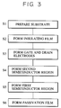
- Fig. 3 is a flowchart showing a manufacture process of the transistor according to the present invention.
- Fig. 4 is a sectional view showing a manufacture step of an LDD-MOS transistor according to a first example of the present invention.
- Fig. 5 is a sectional view showing a manufacture step of the LDD-MOS transistor according to the first example of the present invention.
- Fig. 6 is a sectional view showing a manufacture step of the LDD-MOS transistor according to the first example of the present invention.
- Fig. 7 is a sectional view showing a manufacture step of the LDD-MOS transistor according to the first example of the present invention.
- Fig. 8 is a sectional view showing a manufacture step of the LDD-MOS transistor according to the first example of the present invention.
- Fig. 9 is a sectional view showing a manufacture step of an LDD-MOS transistor according to a second example of the present invention.
- Fig. 10 is a sectional view showing a manufacture step of the LDD-MOS transistor according to the second example of the present invention.
- Fig. 11 is a sectional view showing a manufacture step of the LDD-MOS transistor according to the second example of the present invention.
- Fig. 12 is a sectional view showing a manufacture step of the LDD-MOS transistor according to the second example of the present invention.
- Fig. 13 is a sectional view showing a manufacture step of the LDD-MOS transistor according to the second example of the present invention.
- Fig. 14 is a sectional view showing a manufacture step of an LDD-MOS transistor according to a third example of the present invention.
- Fig. 15 is a sectional view showing a manufacture step of the LDD-MOS transistor according to the third example of the present invention.
- Fig. 16 is a sectional view showing a manufacture step of the LDD-MOS transistor according to the third example of the present invention.
- Fig. 17 is a sectional view showing a manufacture step of the LDD-MOS transistor according to the third example of the present invention.
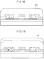
- Fig. 18 is a sectional view showing a manufacture step of the LDD-MOS transistor according to the third example of the present invention.
- Fig. 19 is a sectional view showing a manufacture step of the LDD-MOS transistor according to the third example of the present invention.
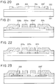
- Fig. 20 is a sectional view showing a manufacture step of an LDD-MOS transistor according to a fourth example of the present invention.
- Fig. 21 is a sectional view showing a manufacture step of the LDD-MOS transistor according to the fourth example of the present invention.
- Fig. 22 is a sectional view showing a manufacture step of the LDD-MOS transistor according to the fourth example of the present invention.
- Fig. 23 is a sectional view showing a manufacture step of the LDD-MOS transistor according to the fourth example of the present invention.
- Fig. 24 is a sectional view showing a manufacture step of the LDD-MOS transistor according to the fourth example of the present invention.
- Fig. 25 is a sectional view showing a manufacture step of the LDD-MOS transistor according to the fourth example of the present invention.
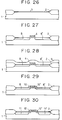
- Fig. 26 is a sectional view Showing a manufacture step of a conventional LDD-MOS transistor.
- Fig. 27 is a sectional view showing a manufacture step of the conventional LDD-MOS transistor.
- Fig. 28 is a sectional view showing a manufacture step of the conventional LDD-MOS transistor.
- Fig. 29 is a sectional view showing a manufacture step of the conventional LDD-MOS transistor.
- Fig. 30 is a sectional view showing a manufacture step of the conventional LDD-MOS transistor.
- Fig. 1 is a schematic plan view showing a transistor according to one preferred embodiment of the present invention and Fig. 2 is a sectional view taken along the line A-A in Fig. 1.
- denoted by reference numeral 21 is a substrate
- 22 is a semiconductor body having a channel region
- 24 is a first semiconductor region having high impurity concentration which serves as a drain
- 26 is a second semiconductor region having low impurity concentration which also serves as a drain.
- Denoted by 25, 27 are sources which are formed, as needed, in a like manner to the drains.
- Denoted by 28 is a gate insulating film
- 29 is a gate electrode
- 30 is a drain electrode
- 31 is a source electrode.
- Denoted by 32 is a passivation film.
- CONT in Fig. 1 denotes a contact hole provided, as needed, for each of the electrodes.
- a drain side edge portion EG1 of the gate electrode 29 and a gate side edge portion EG2 of the drain electrode 30 are self-aligned respectively with opposite edge portions of the second semiconductor region 26.
- edge portions While the corresponding edge portions are shown as perfectly aligning with each other in Fig. 2, there may occur a slight shift between the edge portions due to lateral diffusion of the impurity and oxidation of the gate or drain electrode, because an actual manufacture process often includes heat treatment in which heat is applied to the transistor. Such a shift between the edge portions is on the order of sub-microns or several nanometers, and transistors having shifts on that order are also involved in the present invention.
- Fig. 3 is a flowchart showing one embodiment of a manufacture process of the transistor according to the present invention.
- the substrate 21 is prepared.
- the substrate 21 includes the semiconductor body 22.
- the insulating film 28 is formed on the semiconductor body 22.
- the insulating film 28 has an opening in a position where the drain electrode 30 is to be formed, and the semiconductor body is exposed in the opening.
- the gate electrode 29 and the drain electrode 30 are formed.
- an impurity is doped to form the second semiconductor region 26.
- the impurity is selected so that the second semiconductor region 26 and the channel region 23 have opposite conductivity types. If the channel region 23 has P-type conductivity, the impurity is selected so as to become a donor. Conversely, if it has N-type conductivity, the impurity is selected so as to become an acceptor.
- Step S5 the first semiconductor region 24 is formed. After that, the passivation film is formed as needed. (Step S6).
- the substrate 21 used in the present invention is preferably formed of a semiconductor or insulator.
- a semiconductor it is advantageous to employ a single crystal wafer which is in unitary structure with the semiconductor body 22.
- an SOI base plate is advantageously employed.
- the drains 24, 26 are formed of a semiconductor having the opposite conductivity to that of the channel region 23 and are designed so that the first semiconductor region 24 has higher impurity concentration than the second semiconductor region 26.
- the drains 24, 26 have P-type conductivity and the channel region 23 has N-type conductivity.
- the drains 24, 26 have N-type conductivity.
- the insulating film 28 under the gate electrode 29 includes a portion which functions as a gate insulating film.
- the insulating film is preferably formed of an oxide film, a nitride film or the like.
- the gate electrode 29 is made of a metal such as aluminum (Al), chromium (Cr), molybdenum (Mo), tantalum (Ta), platinum (Pt), tungsten (W), titanium (Ti) and copper (Cu), an alloy of two or more selected from among those metals, an alloy containing any of those metals as a main ingredient and other element (such as Si), or a semiconductor doped with an impurity of high concentration.
- a suitable material having an optimum work function in view of required transistor characteristics.
- polycrystalline silicon as a doped semiconductor is advantageously employed.
- the drain electrode 30 is made of a material having an impurity to be doped into the first semiconductor region 24. In many cases, polycrystalline silicon containing an impurity is advantageously employed.
- the passivation film 32 which is formed, as needed, is made of an inorganic insulator such as silicon oxide and silicon nitride, or an organic insulator such as polyimide, polyamide, epoxy and silicone resin.
- Step S1 is carried out as, for example, a step of depositing the body 22 on a wafer through epitaxial growth, a step of forming a polycrystalline semiconductor on a quartz base plate, or a step of growing single crystal silicon on a sapphire base plate.
- Step S1 includes solid or liquid phase growth of polycrystalline silicon with laser annealing or heat treatment.
- Step S2 is carried out by thermal oxidation or vapor phase deposition.
- Step S2 also includes a step of forming an opening by etching after deposition of the insulating film, or a step of forming a patterned insulating film while masking part of the body 22 which will be an opening.
- Step S3 includes steps of depositing a conductor (including a heavily-doped semiconductor) for the gate electrode and the drain electrode, and patterning a deposited conductor film by etching, or steps of masking a predetermined region and selectively depositing a conductor in a region other than the masked region, as with the lift-off process.
- a conductor including a heavily-doped semiconductor
- the gate electrode and the drain electrode may be formed separately in different steps.
- the gate and drain electrodes are preferably formed by depositing a material common to both the electrodes and patterning the deposited material by photolithography.
- An exposure apparatus used for photolithography in that case may be of an excimer laser emitting a beam of light having wavelength of at least one selected from among 157 nm, 193 nm, 222 nm, 248 nm, 284 nm, 308 nm, 342 nm, 351 nm and 353 nm, or a stepper utilizing ultraviolet rays (i-rays).
- excimer laser exposure is suitable for the present invention in point of further improving the patterning accuracy.
- the second semiconductor region 26 is preferably formed by implanting impurity ions, i.e., ion implantation, with the gate and drain electrodes used as a mask.
- impurity ions i.e., ion implantation
- the active region, etc. which do not require high accuracy may be masked by using a resist as mask material, if necessary, as indicated by MSK in Fig. 1.
- a resist is not required for making the active region.
- Step S5 includes a step of diffusing the impurity from the drain electrode into the underlying body with heat treatment.
- Step S6 includes a step of thermal oxidation or vapor phase deposition.
- the vapor phase deposition can be performed by sputtering or CVD.
- Step S6 is carried out by spin coating or printing.
- the impurity used in the present invention is given by an element of Group V of the Periodic Table, such as phosphorus (P) and arsenic (As), or an element of Group III of the Periodic Table, such as boron (B) and aluminum (Al).
- an element of Group V of the Periodic Table such as phosphorus (P) and arsenic (As)
- an element of Group III of the Periodic Table such as boron (B) and aluminum (Al).
- a liquid crystal panel is formed by placing a liquid crystal between a substrate including the transistors manufactured according to the present invention and a transparent plate such as a glass base plate, a good liquid crystal device of TFT active matrix type can be provided.
- the transistors of the present invention as transistors disposed at intersects between matrix electrodes, and in at least part of a peripheral driving circuit for transmitting a video signal to signal lines.
- P-channel transistors and N-channel transistors in which semiconductors have opposite conductivity types to each other, are arranged on a common substrate in mixed fashion.
- Figs. 4 to 8 are sectional views showing a first example of the manufacture method of the insulated gate transistor according to the present invention. These figures show best features of the present invention. A description will now be made on manufacture steps of this Example with reference to Figs. 4 to 8.
- the LDD-MOS transistor manufactured through the above steps exhibits good controllability because the lightly-doped regions are each formed in a self-aligned manner with the aid of the gate electrode and the drain or source electrode.
- Figs. 9 to 13 are sectional views showing a second example of the manufacture method of the insulated gate transistor according to the present invention. A description will now be made on manufacture steps of this Example with reference to Figs. 4 to 8.
- the film 15 is partly etched away through patterning in regions where an electrode for the source region is to be formed and the polycrystalline silicon wiring is to be connected to an upper wiring, thereby forming openings in those regions.
- a wiring material primarily consisted of Al is formed by sputtering and then patterned to form wirings 16, 16', thereby completing an LDD-MOS transistor (Fig. 13).
- the LDD-MOS transistor manufactured through the above steps exhibits good controllability because the lightly-doped region is formed in a self-aligned manner with the aid of the gate electrode and the drain electrode.
- Figs. 14 to 19 are sectional views showing a third example of the manufacture method of the insulated gate transistor according to the present invention.
- This Example intends to form a thin film transistor (hereinafter referred to as TFT) by utilizing the present invention.
- TFT thin film transistor
- the LDD type TFT manufactured through the above steps has advantages that a leak current, particularly when the TFT is in a non-conducted state, is not affected by misalignment possibly occurred in the photolithography process and is stably produced with good reproducibility, because the size of the lightly-doped regions can be determined in a self-aligned manner.
- the TFT When the TFT is employed as a bidirectional switch, almost the same characteristics are obtained even after the drain and the source are replaced by each other. This is preferable from the viewpoint of circuit design.
- the silicon substrate 101 having the silicon oxide film 102 on its surface may be replaced by a glass or quartz base plate.
- a glass base plate it is desired to carry out the subsequent heat treatment at temperature not higher than 600 °C.
- the polycrystalline silicon film 103 may be formed by solid phase epitaxy of amorphous silicon deposited by CVD, or by re-crystallization of the amorphous silicon using a laser.
- the gate oxide film 104 can also be formed by CVD or sputtering other than thermal oxidation.
- a silicon nitride film may be used instead of the oxide film.
- this Example is applicable to a p-channel TFT as well by using ions all of which have P-type conductivity.
- Figs. 20 to 25 are sectional views showing a fourth example of the manufacture method of the insulated gate transistor according to the present invention.
- the present invention is applied to the manufacture process of a TFT as with the above third Example.
- This Example intends for application to the manufacture process of a TFT having a "dual gate” structure wherein a gate electrode at the same potential is divided into two parts in the direction of channel length so that a leak current through the TFT in an off-state can be reduced and the yield of transistors can be improved.
- the TFT of this Example can be manufactured by employing exactly the same steps as in the above third Example. Because of the specific structure of the TFT, however, the gate electrode of polycrystalline silicon is divided into two portions 206a, 206a' (Fig. 21), and lightly-doped layers are formed not only in regions 207a, 207c respectively contacting the main drain and source regions, but also in a region 207b between the two gate electrodes (Fig. 22).
- This invention provides a transistor manufacture method comprising the steps of forming, on a semiconductor substrate, an insulating film being made open at least in an introducing portion through which an impurity for forming a drain region other than a lightly-doped region is introduced, then forming a gate electrode and a drain electrode each containing an impurity, and then introducing the impurity through between the gate electrode and the drain electrode to thereby form the lightly-doped region; and introducing the impurity from the drain electrode through the impurity introducing portion with heat treatment, to thereby form the drain region.
- a transistor manufactured by the above method is also provided.
Landscapes
- Thin Film Transistor (AREA)
- Insulated Gate Type Field-Effect Transistor (AREA)
Applications Claiming Priority (4)
| Application Number | Priority Date | Filing Date | Title |
|---|---|---|---|
| JP580895 | 1995-01-18 | ||
| JP5808/95 | 1995-01-18 | ||
| JP7312344A JPH08255907A (ja) | 1995-01-18 | 1995-11-30 | 絶縁ゲート型トランジスタ及びその製造方法 |
| JP312344/95 | 1995-11-30 |
Publications (2)
| Publication Number | Publication Date |
|---|---|
| EP0723286A2 true EP0723286A2 (fr) | 1996-07-24 |
| EP0723286A3 EP0723286A3 (fr) | 1998-07-29 |
Family
ID=26339810
Family Applications (1)
| Application Number | Title | Priority Date | Filing Date |
|---|---|---|---|
| EP96100563A Ceased EP0723286A3 (fr) | 1995-01-18 | 1996-01-16 | Transistor à effet de champ et méthode de fabrication |
Country Status (3)
| Country | Link |
|---|---|
| US (1) | US5913111A (fr) |
| EP (1) | EP0723286A3 (fr) |
| JP (1) | JPH08255907A (fr) |
Cited By (9)
| Publication number | Priority date | Publication date | Assignee | Title |
|---|---|---|---|---|
| WO1998049729A1 (fr) * | 1997-04-25 | 1998-11-05 | Vlsi Vision Limited | Detecteur d'image a semi-conducteurs ameliore |
| EP0871227A3 (fr) * | 1997-04-08 | 1999-12-08 | Matsushita Electric Industrial Co., Ltd. | Transistor à couche mince, son procédé de fabrication et son utilisation dans un dispositif d'affichage à cristaux liquides |
| GB2358083A (en) * | 2000-01-07 | 2001-07-11 | Seiko Epson Corp | Thin film transistors |
| US6548356B2 (en) | 2000-01-07 | 2003-04-15 | Seiko Epson Corporation | Thin film transistor |
| US7157317B2 (en) | 2001-10-31 | 2007-01-02 | Semiconductor Energy Laboratory Co., Ltd. | Manufacturing method for field-effect transistor |
| US7807500B2 (en) | 1998-07-29 | 2010-10-05 | Semiconductor Energy Laboratory Co., Ltd. | Process for production of SOI substrate and process for production of semiconductor device including the selective forming of porous layer |
| US8008693B2 (en) | 1996-02-23 | 2011-08-30 | Semiconductor Energy Laboratory Co., Ltd. | Semiconductor thin film and method of manufacturing the same and semiconductor device and method of manufacturing the same |
| US8405090B2 (en) | 1998-09-04 | 2013-03-26 | Semiconductor Energy Labortory Co., Ltd. | Method of fabricating a semiconductor device |
| CN110265481A (zh) * | 2018-08-10 | 2019-09-20 | 友达光电股份有限公司 | 晶体管装置 |
Families Citing this family (24)
| Publication number | Priority date | Publication date | Assignee | Title |
|---|---|---|---|---|
| JP3645380B2 (ja) | 1996-01-19 | 2005-05-11 | 株式会社半導体エネルギー研究所 | 半導体装置の作製方法、情報端末、ヘッドマウントディスプレイ、ナビゲーションシステム、携帯電話、ビデオカメラ、投射型表示装置 |
| JP3645378B2 (ja) | 1996-01-19 | 2005-05-11 | 株式会社半導体エネルギー研究所 | 半導体装置の作製方法 |
| JP3645379B2 (ja) | 1996-01-19 | 2005-05-11 | 株式会社半導体エネルギー研究所 | 半導体装置の作製方法 |
| JP3729955B2 (ja) | 1996-01-19 | 2005-12-21 | 株式会社半導体エネルギー研究所 | 半導体装置の作製方法 |
| US6478263B1 (en) | 1997-01-17 | 2002-11-12 | Semiconductor Energy Laboratory Co., Ltd. | Semiconductor device and its manufacturing method |
| US6180439B1 (en) | 1996-01-26 | 2001-01-30 | Semiconductor Energy Laboratory Co., Ltd. | Method for fabricating a semiconductor device |
| US7056381B1 (en) | 1996-01-26 | 2006-06-06 | Semiconductor Energy Laboratory Co., Ltd. | Fabrication method of semiconductor device |
| US6100562A (en) * | 1996-03-17 | 2000-08-08 | Semiconductor Energy Laboratory Co., Ltd. | Method of manufacturing a semiconductor device |
| JPH11112002A (ja) * | 1997-10-07 | 1999-04-23 | Semiconductor Energy Lab Co Ltd | 半導体装置およびその製造方法 |
| US6686623B2 (en) | 1997-11-18 | 2004-02-03 | Semiconductor Energy Laboratory Co., Ltd. | Nonvolatile memory and electronic apparatus |
| US6444390B1 (en) * | 1998-02-18 | 2002-09-03 | Semiconductor Energy Laboratory Co., Ltd. | Process for producing semiconductor thin film devices using group 14 element and high temperature oxidizing treatment to achieve a crystalline silicon film |
| US6396147B1 (en) * | 1998-05-16 | 2002-05-28 | Semiconductor Energy Laboratory Co., Ltd. | Semiconductor device with metal-oxide conductors |
| JP2000012864A (ja) | 1998-06-22 | 2000-01-14 | Semiconductor Energy Lab Co Ltd | 半導体装置の作製方法 |
| US7030430B2 (en) * | 2003-08-15 | 2006-04-18 | Intel Corporation | Transition metal alloys for use as a gate electrode and devices incorporating these alloys |
| US7018012B2 (en) * | 2003-11-14 | 2006-03-28 | Lexmark International, Inc. | Microfluid ejection device having efficient logic and driver circuitry |
| JP4482428B2 (ja) * | 2004-11-12 | 2010-06-16 | 川崎マイクロエレクトロニクス株式会社 | 半導体集積回路の製造方法および半導体集積回路 |
| JP5200399B2 (ja) * | 2007-03-26 | 2013-06-05 | 富士通セミコンダクター株式会社 | Mosトランジスタの製造方法 |
| KR100875432B1 (ko) | 2007-05-31 | 2008-12-22 | 삼성모바일디스플레이주식회사 | 다결정 실리콘층의 제조 방법, 이를 이용하여 형성된박막트랜지스터, 그의 제조방법 및 이를 포함하는유기전계발광표시장치 |
| KR100889626B1 (ko) | 2007-08-22 | 2009-03-20 | 삼성모바일디스플레이주식회사 | 박막트랜지스터, 그의 제조방법, 이를 구비한유기전계발광표시장치, 및 그의 제조방법 |
| KR100889627B1 (ko) | 2007-08-23 | 2009-03-20 | 삼성모바일디스플레이주식회사 | 박막트랜지스터, 그의 제조방법, 및 이를 구비한유기전계발광표시장치 |
| KR100982310B1 (ko) | 2008-03-27 | 2010-09-15 | 삼성모바일디스플레이주식회사 | 박막트랜지스터, 그의 제조방법, 및 이를 포함하는유기전계발광표시장치 |
| KR100989136B1 (ko) | 2008-04-11 | 2010-10-20 | 삼성모바일디스플레이주식회사 | 박막트랜지스터, 그의 제조방법, 및 이를 포함하는유기전계발광표시장치 |
| JP5369018B2 (ja) * | 2010-02-17 | 2013-12-18 | シャープ株式会社 | Misfet製造方法 |
| TWI570920B (zh) * | 2011-01-26 | 2017-02-11 | 半導體能源研究所股份有限公司 | 半導體裝置及其製造方法 |
Family Cites Families (17)
| Publication number | Priority date | Publication date | Assignee | Title |
|---|---|---|---|---|
| JPS567304B2 (fr) * | 1972-08-28 | 1981-02-17 | ||
| US4016587A (en) * | 1974-12-03 | 1977-04-05 | International Business Machines Corporation | Raised source and drain IGFET device and method |
| US4069067A (en) * | 1975-03-20 | 1978-01-17 | Matsushita Electric Industrial Co., Ltd. | Method of making a semiconductor device |
| US4341009A (en) * | 1980-12-05 | 1982-07-27 | International Business Machines Corporation | Method for making an electrical contact to a silicon substrate through a relatively thin layer of silicon dioxide on the surface of the substrate |
| JPS58202525A (ja) * | 1982-05-21 | 1983-11-25 | Toshiba Corp | 半導体装置の製造方法 |
| KR890004962B1 (ko) * | 1985-02-08 | 1989-12-02 | 가부시끼가이샤 도오시바 | 반도체장치 및 그 제조방법 |
| US4731318A (en) * | 1985-02-26 | 1988-03-15 | Societe Pour L'etude Et La Fabrication Des Circuits Integres Speciaux - E.F.C.I.S. | Integrated circuit comprising MOS transistors having electrodes of metallic silicide and a method of fabrication of said circuit |
| JP2633541B2 (ja) * | 1987-01-07 | 1997-07-23 | 株式会社東芝 | 半導体メモリ装置の製造方法 |
| JPH0194666A (ja) * | 1987-10-06 | 1989-04-13 | Oki Electric Ind Co Ltd | Mosfetの製造方法 |
| US4945070A (en) * | 1989-01-24 | 1990-07-31 | Harris Corporation | Method of making cmos with shallow source and drain junctions |
| US5200639A (en) * | 1990-05-31 | 1993-04-06 | Canon Kabushiki Kaisha | Semiconductor device with isolating groove containing single crystalline aluminum wiring |
| US5262664A (en) * | 1990-06-30 | 1993-11-16 | Goldstar Electron Co., Ltd. | Process for formation of LDD transistor, and structure thereof |
| JPH04354331A (ja) * | 1991-05-31 | 1992-12-08 | Sony Corp | ドライエッチング方法 |
| US5200352A (en) * | 1991-11-25 | 1993-04-06 | Motorola Inc. | Transistor having a lightly doped region and method of formation |
| TW363146B (en) * | 1992-08-20 | 1999-07-01 | Sony Corp | An anti-reflective layer and a method of forming a photoresist pattern |
| KR0150105B1 (ko) * | 1995-06-20 | 1998-12-01 | 김주용 | 반도체 소자의 트랜지스터 제조방법 |
| DE19536249A1 (de) * | 1995-09-28 | 1997-04-10 | Siemens Ag | Verfahren zur Herstellung einer Vielzahl von mikroelektronischen Schaltungen auf SOI |
-
1995
- 1995-11-30 JP JP7312344A patent/JPH08255907A/ja active Pending
-
1996
- 1996-01-16 EP EP96100563A patent/EP0723286A3/fr not_active Ceased
- 1996-01-17 US US08/587,661 patent/US5913111A/en not_active Expired - Fee Related
Cited By (16)
| Publication number | Priority date | Publication date | Assignee | Title |
|---|---|---|---|---|
| US8008693B2 (en) | 1996-02-23 | 2011-08-30 | Semiconductor Energy Laboratory Co., Ltd. | Semiconductor thin film and method of manufacturing the same and semiconductor device and method of manufacturing the same |
| EP0871227A3 (fr) * | 1997-04-08 | 1999-12-08 | Matsushita Electric Industrial Co., Ltd. | Transistor à couche mince, son procédé de fabrication et son utilisation dans un dispositif d'affichage à cristaux liquides |
| US6034748A (en) * | 1997-04-08 | 2000-03-07 | Matsushita Electric Industrial Co., Ltd. | Thin film transistor, manufacturing method therefor and liquid crystal display unit using the same |
| WO1998049729A1 (fr) * | 1997-04-25 | 1998-11-05 | Vlsi Vision Limited | Detecteur d'image a semi-conducteurs ameliore |
| US8642405B2 (en) | 1998-07-29 | 2014-02-04 | Semiconductor Energy Laboratory Co., Ltd. | Process for production of SOI substrate and process for production of semiconductor device |
| US7807500B2 (en) | 1998-07-29 | 2010-10-05 | Semiconductor Energy Laboratory Co., Ltd. | Process for production of SOI substrate and process for production of semiconductor device including the selective forming of porous layer |
| US9070604B2 (en) | 1998-09-04 | 2015-06-30 | Semiconductor Energy Laboratory Co., Ltd. | Method of fabricating a semiconductor device |
| US8405090B2 (en) | 1998-09-04 | 2013-03-26 | Semiconductor Energy Labortory Co., Ltd. | Method of fabricating a semiconductor device |
| GB2358083A (en) * | 2000-01-07 | 2001-07-11 | Seiko Epson Corp | Thin film transistors |
| US6548356B2 (en) | 2000-01-07 | 2003-04-15 | Seiko Epson Corporation | Thin film transistor |
| US6580129B2 (en) | 2000-01-07 | 2003-06-17 | Seiko Epson Corporation | Thin-film transistor and its manufacturing method |
| GB2358083B (en) * | 2000-01-07 | 2004-02-18 | Seiko Epson Corp | Thin-film transistor and its manufacturing method |
| US7718478B2 (en) | 2001-10-31 | 2010-05-18 | Semiconductor Energy Laboratory Co., Ltd. | Manufacturing method for field-effect transistor |
| US8420461B2 (en) | 2001-10-31 | 2013-04-16 | Semiconductor Energy Laboratory Co., Ltd. | Manufacturing method for field-effect transistor |
| US7157317B2 (en) | 2001-10-31 | 2007-01-02 | Semiconductor Energy Laboratory Co., Ltd. | Manufacturing method for field-effect transistor |
| CN110265481A (zh) * | 2018-08-10 | 2019-09-20 | 友达光电股份有限公司 | 晶体管装置 |
Also Published As
| Publication number | Publication date |
|---|---|
| US5913111A (en) | 1999-06-15 |
| JPH08255907A (ja) | 1996-10-01 |
| EP0723286A3 (fr) | 1998-07-29 |
Similar Documents
| Publication | Publication Date | Title |
|---|---|---|
| US5913111A (en) | Method of manufacturing an insulaed gate transistor | |
| US5998838A (en) | Thin film transistor | |
| US7118944B2 (en) | Method for fabricating polycrystalline silicon thin film transistor | |
| US5328861A (en) | Method for forming thin film transistor | |
| US6232158B1 (en) | Thin film transistor and a fabricating method thereof | |
| US7709904B2 (en) | Thin film transistor substrate and method for manufacturing the same | |
| US7795082B2 (en) | Method of fabricating thin film transistor | |
| US7306980B2 (en) | Method for fabricating thin film transistor | |
| JPH05335573A (ja) | 薄膜半導体装置 | |
| US7714387B2 (en) | Semiconductor device with thin-film transistors and method of fabricating the same | |
| US5879976A (en) | Thin film transistor and method for producing the same | |
| US5677207A (en) | Method for fabricating a thin film transistor using silicide layer | |
| JPH07176750A (ja) | 薄膜トランジスターの製造方法 | |
| US20020137310A1 (en) | Method and apparatus for fabricating a semiconductor device | |
| KR19980035159A (ko) | 박막트랜지스터의 구조 및 그 제조방법 | |
| KR20060062139A (ko) | 이중 열처리에 의한 다결정 박막트랜지스터 제조방법 | |
| KR20050042596A (ko) | 폴리실리콘 액정표시소자 및 그 제조방법 | |
| JP2000077665A (ja) | 薄膜トランジスタ装置及び薄膜トランジスタ装置の製造方法 | |
| US20100207120A1 (en) | Production method of semiconductor device and semiconductor device | |
| US6790715B1 (en) | Manufacturing method of CMOS thin film transistor | |
| JP3398665B2 (ja) | 薄膜トランジスタの製造方法 | |
| JP2004336073A (ja) | トップゲート型薄膜トランジスタ及びその製造方法 | |
| KR20040058699A (ko) | 박막 트랜지스터 어레이 기판의 제조 방법 | |
| JP3578424B2 (ja) | アクティブマトリクス基板の製造方法 | |
| JPH09213962A (ja) | 薄膜トランジスタおよびその製造方法 |
Legal Events
| Date | Code | Title | Description |
|---|---|---|---|
| PUAI | Public reference made under article 153(3) epc to a published international application that has entered the european phase |
Free format text: ORIGINAL CODE: 0009012 |
|
| AK | Designated contracting states |
Kind code of ref document: A2 Designated state(s): DE FR GB IT NL |
|
| PUAL | Search report despatched |
Free format text: ORIGINAL CODE: 0009013 |
|
| AK | Designated contracting states |
Kind code of ref document: A3 Designated state(s): DE FR GB IT NL |
|
| 17P | Request for examination filed |
Effective date: 19981211 |
|
| 17Q | First examination report despatched |
Effective date: 20030512 |
|
| STAA | Information on the status of an ep patent application or granted ep patent |
Free format text: STATUS: THE APPLICATION HAS BEEN REFUSED |
|
| 18R | Application refused |
Effective date: 20060316 |