EP0725513B1 - Fehlertolerante Endstufe für ein digitales Zweileiterbus-Datenkommunikationssystem - Google Patents
Fehlertolerante Endstufe für ein digitales Zweileiterbus-Datenkommunikationssystem Download PDFInfo
- Publication number
- EP0725513B1 EP0725513B1 EP96100595A EP96100595A EP0725513B1 EP 0725513 B1 EP0725513 B1 EP 0725513B1 EP 96100595 A EP96100595 A EP 96100595A EP 96100595 A EP96100595 A EP 96100595A EP 0725513 B1 EP0725513 B1 EP 0725513B1
- Authority
- EP
- European Patent Office
- Prior art keywords
- module
- bus
- signals
- stage
- bus lines
- Prior art date
- Legal status (The legal status is an assumption and is not a legal conclusion. Google has not performed a legal analysis and makes no representation as to the accuracy of the status listed.)
- Expired - Lifetime
Links
- 238000004891 communication Methods 0.000 title claims description 13
- 238000012545 processing Methods 0.000 claims description 44
- 238000001514 detection method Methods 0.000 claims description 22
- 230000006978 adaptation Effects 0.000 claims 2
- 230000004069 differentiation Effects 0.000 claims 1
- 230000005540 biological transmission Effects 0.000 description 12
- 238000010586 diagram Methods 0.000 description 10
- 239000003990 capacitor Substances 0.000 description 7
- 238000013459 approach Methods 0.000 description 6
- 238000013461 design Methods 0.000 description 6
- 239000004020 conductor Substances 0.000 description 5
- 238000001914 filtration Methods 0.000 description 3
- 230000003068 static effect Effects 0.000 description 3
- 238000012360 testing method Methods 0.000 description 3
- 238000012546 transfer Methods 0.000 description 3
- 238000011144 upstream manufacturing Methods 0.000 description 2
- 230000000295 complement effect Effects 0.000 description 1
- 238000010276 construction Methods 0.000 description 1
- 230000000694 effects Effects 0.000 description 1
- 238000005516 engineering process Methods 0.000 description 1
- 238000011156 evaluation Methods 0.000 description 1
- 238000007667 floating Methods 0.000 description 1
- 238000000034 method Methods 0.000 description 1
- 230000006855 networking Effects 0.000 description 1
- 230000008569 process Effects 0.000 description 1
- 230000004044 response Effects 0.000 description 1
- 238000004513 sizing Methods 0.000 description 1
- 230000001360 synchronised effect Effects 0.000 description 1
Images

Classifications
-
- H—ELECTRICITY
- H04—ELECTRIC COMMUNICATION TECHNIQUE
- H04L—TRANSMISSION OF DIGITAL INFORMATION, e.g. TELEGRAPHIC COMMUNICATION
- H04L12/00—Data switching networks
- H04L12/28—Data switching networks characterised by path configuration, e.g. LAN [Local Area Networks] or WAN [Wide Area Networks]
- H04L12/40—Bus networks
-
- H—ELECTRICITY
- H04—ELECTRIC COMMUNICATION TECHNIQUE
- H04L—TRANSMISSION OF DIGITAL INFORMATION, e.g. TELEGRAPHIC COMMUNICATION
- H04L12/00—Data switching networks
- H04L12/28—Data switching networks characterised by path configuration, e.g. LAN [Local Area Networks] or WAN [Wide Area Networks]
- H04L12/40—Bus networks
- H04L12/40006—Architecture of a communication node
- H04L12/40032—Details regarding a bus interface enhancer
-
- H—ELECTRICITY
- H04—ELECTRIC COMMUNICATION TECHNIQUE
- H04L—TRANSMISSION OF DIGITAL INFORMATION, e.g. TELEGRAPHIC COMMUNICATION
- H04L25/00—Baseband systems
- H04L25/02—Details ; arrangements for supplying electrical power along data transmission lines
- H04L25/08—Modifications for reducing interference; Modifications for reducing effects due to line faults ; Receiver end arrangements for detecting or overcoming line faults
-
- B—PERFORMING OPERATIONS; TRANSPORTING
- B60—VEHICLES IN GENERAL
- B60R—VEHICLES, VEHICLE FITTINGS, OR VEHICLE PARTS, NOT OTHERWISE PROVIDED FOR
- B60R16/00—Electric or fluid circuits specially adapted for vehicles and not otherwise provided for; Arrangement of elements of electric or fluid circuits specially adapted for vehicles and not otherwise provided for
- B60R16/02—Electric or fluid circuits specially adapted for vehicles and not otherwise provided for; Arrangement of elements of electric or fluid circuits specially adapted for vehicles and not otherwise provided for electric constitutive elements
- B60R16/03—Electric or fluid circuits specially adapted for vehicles and not otherwise provided for; Arrangement of elements of electric or fluid circuits specially adapted for vehicles and not otherwise provided for electric constitutive elements for supply of electrical power to vehicle subsystems or for
- B60R16/0315—Electric or fluid circuits specially adapted for vehicles and not otherwise provided for; Arrangement of elements of electric or fluid circuits specially adapted for vehicles and not otherwise provided for electric constitutive elements for supply of electrical power to vehicle subsystems or for using multiplexing techniques
-
- H—ELECTRICITY
- H04—ELECTRIC COMMUNICATION TECHNIQUE
- H04L—TRANSMISSION OF DIGITAL INFORMATION, e.g. TELEGRAPHIC COMMUNICATION
- H04L12/00—Data switching networks
- H04L12/28—Data switching networks characterised by path configuration, e.g. LAN [Local Area Networks] or WAN [Wide Area Networks]
- H04L12/40—Bus networks
- H04L2012/40208—Bus networks characterized by the use of a particular bus standard
- H04L2012/40215—Controller Area Network CAN
-
- H—ELECTRICITY
- H04—ELECTRIC COMMUNICATION TECHNIQUE
- H04L—TRANSMISSION OF DIGITAL INFORMATION, e.g. TELEGRAPHIC COMMUNICATION
- H04L12/00—Data switching networks
- H04L12/28—Data switching networks characterised by path configuration, e.g. LAN [Local Area Networks] or WAN [Wide Area Networks]
- H04L12/40—Bus networks
- H04L2012/40267—Bus for use in transportation systems
- H04L2012/40273—Bus for use in transportation systems the transportation system being a vehicle
Definitions
- the invention relates to a fault-tolerant power amplifier for a digital two-bus data communication system according to the The preamble of claim 1 of claim 2 and claim 3.
- Such power amplifiers find, for example in motor vehicles within a CAN system use. Equipped with such a power amplifier, each of a plurality of subscriber terminals of the communication system with the others over the two-conductor bus in mutual Communicate traffic in time-division multiplex.
- the two-conductor bus consists of a two-wire line, e.g. in the Vehicle runs within a harness.
- Two-wire data bus can failures in the form of cable breaks or Short circuits of the lines with one or the other supply voltage level or in the form of a short circuit of the two Lines occur against each other.
- Two-wire reception network interface is on Microcomputer upstream, the transmission of test messages monitored and the network interface depending on the detected Bus line state via two provided in their switching elements Switch between two-wire operation and single-wire operation can.
- the invention is the provision as a technical problem a fault-tolerant power amplifier of the type mentioned, based, when an arbitrary single error occurs automatically in real time and without additional software switch from two-conductor to single-conductor operation and thereby the data communication can continue without delay.
- the power amplifier is divided into a transmitting module and a receiving stage, which in turn from a module for intermediate processing of incoming bus signals, a Receiving module and a state recognition module exists.
- the Condition detection module serves to solve the single error of a Short circuit of the two bus lines recognize each other can.
- the intermediate processing module switches the transmission module of a differential Two-wire to a single-wire mode, including the transmitter module provided an associated control input and the transmission module suitable is designed.
- the transmitter module in the operating mode the error-free Bus lines is provided, remain.
- the intermediate processing module is designed so that it is the bus signals for the receiving module both with faultless bus lines as well as with interruption or short to the high or low supply voltage from one of the two bus lines and in the event of a short circuit the two bus lines with each other automatically or controlled by.
- Condition detection module prepared so that the Data information forwarded without delay to the receiving module can be.
- the receiving module then prepares the intermediate processed Data bus signals for a subsequent data processing unit on.
- the invention allows with low circuit complexity, the switching of the transmitter module between the difference and the single-wire mode, in the latter, the L output to a floating voltage state is set.
- this is according to a differential operation approach it is designed between two-wire processing and a one-wire processing on the H-bus switchable is.
- the latter mode is selected when a Short circuit of the two bus lines against each other. to Switching therefore conveniently becomes the output of the state detection module used, which already to the corresponding Mode changeover of the send module is used.
- This in this differential operation approach designed intermediate processing module filters high dynamic and static common mode noise Reliable, which is a use in heavily disturbed data networks allows.
- the intermediate processing module according to a dynamic, mass-related Approach designed. It has to be derived from the bus signals, asymmetric difference forming a three-stage structure with an input-side level adjustment stage, a comparator stage, which the two data bus signals simultaneously and independently further processed with dynamic threshold tracking, and an output level level adjustment stage.
- the thus-designed intermediate processing module is capable of the upcoming Data signals from the bus lines in all operating modes, i.e. in error-free operation as well as in operation with one arbitrary single errors, independently and without delay to prepare for the subsequent receiving module.
- the receiving module from an inverting comparator with the input signal dynamically tracked threshold.
- For the state recognition module is a circuit technology Realization as a difference window comparator with downstream, asymmetric time filtering advantageous.
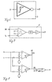
- Fig. 1 is a fault tolerant power amplifier, which is for certificationendstellen a time-division multiplexing CAN system can be used in a motor vehicle, in an overview block diagram shown.
- the power amplifier consists of a Transmitter module (1), which from a data processing unit, not shown incoming, serial data signals (E) in Bus signals for a digital two-wire bus (6) with an H-bus line and transferred to an L bus line.
- At the receiving end contains the power amplifier one to the two data bus lines (H, L) connected receiving stage (2), which consists of an intermediate processing module (3) and a downstream receiving module (4) and an input side in parallel with the intermediate processing module (3) connected to the two data bus lines (H, L)
- Condition detection module (5) consists.
- the intermediate processing module prepares the on the two bus lines (H, L) incoming signals for the downstream receiving module (4) which, in turn, interpolates the intermediate signals (D) in Signals (A) for a subsequent, not shown, data processing unit edited.
- the state recognition module (5) is used the detection of a short circuit of the two data bus lines (6) against each other and gives a corresponding short-circuiting indicator Output signal (Z) from.
- the power amplifier constructed in this way is capable of data communication via the data bus (6) both with error-free bus lines (H, L) as well as any single error in the data bus (6) automatically maintain in real time, without the need for special software algorithms become.
- the seven possible single errors are here Short circuit of the H bus line or the L bus line against the high or the low supply voltage level, an interruption one of the two bus lines (H, L) or a short circuit of H bus line and L bus line against each other.
- the transmission module (1) is designed to be in the first six Error states and in the error-free data bus state in each case a first mode of operation while it is occurring a short circuit of the data bus lines (H, L) with each other, controlled by the state detection module detecting this short circuit (5), changes to a second mode.
- the intermediate processing module (3) is designed so that it's the incoming data information in each of the eight mentioned Data bus states correctly forward to the receiving module able, whereby it depends on the circuit realization in the case of a short circuit of the bus lines (H, L) with each other the data transfer either completely automatically or by switching to another mode, controlled by Condition detection module (5), continues.
- FIGS. 2 to 8 are exemplary implementations of the individual Components of the fault-tolerant final stage of FIG. 1 are shown which the mentioned, required for the respective components Fulfill functions. This will be explained in more detail below received.
- This special dimensioning of the power amplifier has a working range between 10kBd and 125kBd.
- the bit times be between 8 ⁇ s and 100 ⁇ s.
- the bus voltage level are set as follows. In the recessive state the H-bus line has a high resistance of 1.75 V and the L-bus line high impedance at 3.25V.
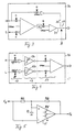
- Fig. 2 shows the circuit construction of the transmission module (1).
- the H output is connected via a high-impedance resistor (Rrh) on a 1.75V power supply as well as a low impedance Resistor (Rdh) and a first controllable switching element (7) on a 5V power supply.
- the switching element (7) is driven by the incoming signal (E).
- the L output is via a low-impedance resistor (Rdl) and a second controllable Switching element (8) to ground and over a high-impedance resistor (Rrl) and a third controllable Switching element (9) on a 3.25V power supply.
- About one fourth controllable switching element (10) controls the input signal (E) the second switching element (8) synchronous with the first Switching element (7). Via a control input is the output signal (Z) can be supplied by the state recognition unit (5), which in the transmission module (1) synchronously the third (9) and the fourth Switching element (10) controls.
- the transmission module (1) realized at mutually shorted bus lines (H, L) the so-called Single-wire operation and in the other bus line states the so-called differential operation.
- the Circuit structure of the transmitter module in particular the resistors, is dimensioned so that specified, maximum settling times be maintained at voltage level changes.
- the intermediate processing module (3a) shown in Fig. 3 is according to a difference approach, where it is high dynamic and reliably filters out static common-mode noise, so it is especially suitable for use in heavily disturbed Networking is suitable.
- the intermediate processing module (3a) has On the output side, a controllable switching element (11), the from the Output signal (Z) of the state detection module (5) controlled whereby the intermediate processing module (3a) between two Operating modes can be switched.
- the switching element (11) is a differential mode before, in which the incoming bus signals (H, L) on the input side for level matching multiplied by a factor (f1) of 1/12 after which the difference takes place.
- the resulting Signal is then in a high pass (HP) of a common mode adjustment subjected and then for level adjustment with a Factor (f6) multiplied by 2 as well as one of the known design principles shifted corresponding offset.
- HP high pass
- f6 Factor
- the signal obtained (D1) is from the driven switching element (11) as an output signal (D) passed. In the state of a short circuit the two bus lines (H, L) against each other controls the state detection unit (5) the switching element (11) in the other Switching position.
- the output signal (D) formed by a signal obtained solely from the H bus line (D2), why the H signal for level adjustment with a factor (f2) multiplied by 1/6 and one of the known design principles corresponding offset is shifted.
- the intermediate processing module (3a) with the circuit structure of FIG. 3 is thus between the state detection module (5) between differential operation and one-wire operation switched.
- the illustrated in Fig. 4 realization of an intermediate processing module (3b) also makes an autonomous adjustment to the Status of shorted bus lines (H, L) and so that in all eight mentioned line conditions.
- This intermediate processing module (3b) has a three-stage structure with an input-side level adjustment stage (12), a central Comparator stage (13) and an output-side level adjustment stage (14).
- the input-side level adjustment stage (12) the incoming bus signals (H, L) are each disconnected from each other with a factor (f3) of -1/6 and a factor (f7) multiplied by 1/6 and one the known design principles shifted corresponding offset.
- the subsequent comparator stage (13) become the pretreated signals simultaneously and independently with the help of a comparator (13a, 13b) evaluated with dynamic threshold tracking.
- the threshold is from the idle state of the incoming Signals corresponding to a suitably chosen time constant and a suitably chosen voltage gap derived.
- FIG. 5 A possible implementation that can be used for the two identical comparators (13a, 13b) of this intermediate processing module (3b) is shown in FIG. 5 in the detailed circuit diagram.
- the implementation of this comparator includes a comparator IC (15) and two resistors (R1, R2) and a capacitor (C).
- the two resistors (R1, R2) form a voltage divider between input signal (K E ) and output signal (K A ).
- the comparator threshold is derived from the input signal (K E ).
- the inverting input of the comparator IC is directly applied to the input signal (K E )
- its non-inverting input is connected to the center tap of the voltage divider, with the capacitor (C) between this center tap and ground.
- the response time of the dynamic threshold is determined.
- a wiring as an inverter allows a simple circuit design.
- the two separate output signals of the comparator stage (13) are then in the subsequent level adjustment stage (14) for Output signal (D) of the intermediate processing module (3b) further processed.
- the intermediate processing module (3b) is capable of incoming data information both error-free bus lines (H, L) as well as any of the above seven Single error in one of the downstream receiving module (4) convert evaluable output signal (D).
- FIG. 6 shows an implementation for the receiving module (4). which the output signal (D) of the intermediate processing unit (3) into an output signal (A) transferred from a subsequent data processing unit can be evaluated.
- the realization shown corresponds identically to the circuit structure each of the two comparators (13a, 13b) of the comparator stage (13) of the intermediate processing module (3b) of Fig. 4.
- the means that the receiving module (4) according to FIG. 6 consists of a comparator IC, two resistors and a capacitor with the in Fig. 5 shown circuit structure and thus has the function an inverting comparator with the input signal (D) dynamically tracked threshold.
- FIG. 7 shows First, the rough structure of the state recognition module (5) with an input side difference window comparator with two selectable thresholds (S1, S2) and from a subsequent stage for asymmetric time filtering.
- FIG 8 is the circuit structure reproduced in more detail.
- the difference window comparator part includes one comparator for each threshold (S1, S2), wherein the incoming H and L bus signals the one Comparator reversed to the other input side are supplied via respective resistors. At the same time are over respective resistors both noninverting comparator inputs and the inverting comparator inputs each with a predetermined voltage level connected.
- the comparator stage is For example, the voltage interval between -0.5V and + 0.5V dimensioned.
- For asymmetric time filtering are the output side merged comparator signals between two Resistors (R3, R4) placed in series between a 5V supply voltage and the noninverting input of a subsequent comparator are looped, wherein the non-inverting Comparator input in addition via a capacitor (C2) is grounded while the inverting comparator input is subjected to a 2.5V voltage.
- the output signal the thus-constructed state recognition unit (5) indicative thereof is whether the differential voltage between H bus line and L bus line longer than the short, second time constant a given Value falls short, causing the case of a short circuit the H-bus line against the L-bus line clearly detectable is.
- the shown fault tolerant power amplifier maintaining data communication in the CAN system of the motor vehicle not only in error-free Bus lines, but also when a single fault occurs in real time independently and without additional software effort guaranteed. In case of error, the power amplifier switches automatically from differential to single-wire operation. It is understood that the power amplifier is the same for other digital data communication systems suitable with a two-conductor bus.
Landscapes
- Engineering & Computer Science (AREA)
- Computer Networks & Wireless Communication (AREA)
- Signal Processing (AREA)
- Power Engineering (AREA)
- Dc Digital Transmission (AREA)
- Maintenance And Management Of Digital Transmission (AREA)
Description
- Fig. 1
- ein schematisches Blockschaltbild einer fehlertoleranten Endstufe für ein CAN-System eines Kraftfahrzeuges,
- Fig. 2
- ein detaillierteres Schaltbild eines in der Endstufe von Fig. 1 verwendeten Sendemoduls,
- Fig. 3
- ein detaillierteres Schaltbild einer ersten schaltungstechnischen Realisierung eines in der Endstufe von Fig. 1 verwendeten Zwischenverbarbeitungsmoduls,
- Fig. 4
- ein detaillierteres Schaltbild einer zweiten schaltungstechnischen Realisierung des in der Endstufe von Fig. 1 vorgesehenen Zwischenverarbeitungsmoduls,
- Fig. 5
- ein detaillierteres Schaltbild einer in dem Zwischenverarbeitungsmodul von Fig. 4 verwendeten Komparatorschaltung,
- Fig. 6
- ein detaillierteres Blockschaltbild einer in der Endstufe von Fig. 1 verwendeten Empfangsstufe,
- Fig. 7
- ein Funktionsblock-Schaltbild eines in der Endstufe von Fig. 1 verwendeten Zustandserkennungsmoduls und
- Fig. 8
- ein detaillierteres Schaltbild des Zustandserkennungsmoduls gemäß Fig. 7.
Claims (5)
- Fehlertolerante Endstufe für ein digitales Zweileiterbus-Datenkommunikationssystem mit einem Sendemodul (1), das ankommende serielle Datensignale (E) in Signale für eine H- und eine L-Busleitung umwandelt, und einer Empfangsstufe (2) mit einem eingangsseitig an die Busleitungen (H, L) angeschlossenen Zwischenverarbeitungsmodul (3, 3a) und einem nachgeschalteten Empfangsmodul (4), das die zwischenverarbeiteten Bussignale für eine nachgeschaltete Datenverarbeitungseinheit aufbereitet, dadurch gekennzeichnet, daß
ein an die Busleitungen (H, L) angeschlossenes Zustandserkennungsmodul (5) zur Erkennung eines Kurzschlußzustands der Busleitungen untereinander vorgesehen ist, das Sendemodul (1) ein vom kurzschlußindikativen Ausgangssignal (Z) des Zustandserkennungsmoduls gesteuertes Schaltmittel zum Schalten zwischen einer Differenz- und einer Eindrahtbetriebsart aufweist und daß das Zwischenverarbeitungsmodul (3, 3a) ein Mittel zum Aufbereiten der Bussignale für das Empfangsmodul (4) aufweist und vom Ausgangssignal des Zustandserkennungsmoduls (5) zur Umschaltung zwischen zwei Betriebsarten ansteuerbar ist, wobei es in einer ersten Betriebsart aus den beiden Busleitungssignalen (H, L) ein pegelangepaßtes und um einen Gleichspannungsanteil bereinigtes Differenzsignal (D1) und in der anderen Betriebsart ein pegelangepaßtes Signal (D2) aus der H-Busleitung erzeugt. - Fehlertolerante Endstufe für ein digitales Zweileiterbus-Datenkommunikationssystem mit einem Sendemodul (1), das ankommende serielle Datensignale (E) in Signale für eine H- und eine L-Busleitung umwandelt, und einer Empfangsstufe (2) mit einem eingangsseitig an die Busleitungen (H, L) angeschlossenen Zwischenverarbeitungsmodul (3, 3b) und einem nachgeschalteten Empfangsmodul (4), das die zwischenverarbeiteten Bussignale für eine nachgeschaltete Datenverarbeitungseinheit aufbereitet, dadurch gekennzeichnet, daß
ein an die Busleitungen (H, L) angeschlossenes Zustandserkennungsmodul (5) zur Erkennung eines Kurzschlußzustands der Busleitungen untereinander vorgesehen ist, das Sendemodul (1) ein vom kurzschlußindikativen Ausgangssignal (Z) des Zustandserkennungsmoduls gesteuertes Schaltmittel zum Schalten zwischen einer Differenz- und einer Eindrahtbetriebsart aufweist und daß das Zwischenverarbeitungsmodul (3, 3b) ein Mittel zum Aufbereiten der Bussignale für das Empfangsmodul (4) aufweist und zur aus den Busleitungssignalen (H, L) abgeleiteten Differenzbildung einen dreistufigen Aufbau mit einer eingangsseitigen Pegelanpassungsstufe (12), einer nachgeschalteten Signalvergleichsstufe (13) mit für jede Busleitung getrennt je einem mitgekoppelten Vergleichsmittel (13a, 13b) sowie einer ausgangsseitigen Pegelanpassungsstufe (14) besitzt. - Endstufe nach Anspruch 1, dadurch gekennzeichnet, daß das Sendemodul (1) ein oder mehrere vom Zustandserkennungsmodul (5) ansteuerbare Schaltelemente (9, 10) aufweist, durch welche der L-Ausgang in der einen Schaltstellung hochohmig an einen Zwischenspannungspegel angeschlossen und niederohmig über ein vom Eingangssignal (E) ansteuerbares Schaltelement (8) mit einem niederen Spannungspegel verbindbar ist und in der anderen Schaltstellung von beiden Spannungspegeln abgekoppelt ist.
- Endstufe nach einem der vorhergehenden Ansprüche, dadurch gekennzeichnet, daß das Empfangsmodul (4) durch einen mitgekoppelten Komparator mit dynamischer Schwellennachführung gebildet ist.
- Endstufe nach einem der vorhergehenden Ansprüche, dadurch gekennzeichnet, daß das Zustandserkennungsmodul als Differenz-Fensterkomparator mit nachgeschalteter asymetrischer Zeitfilterungseinheit realisiert ist.
Applications Claiming Priority (2)
| Application Number | Priority Date | Filing Date | Title |
|---|---|---|---|
| DE19503460 | 1995-02-03 | ||
| DE19503460A DE19503460C1 (de) | 1995-02-03 | 1995-02-03 | Fehlertolerante Endstufe für ein digitales Zweileiterbus-Datenkommunikationssystem |
Publications (2)
| Publication Number | Publication Date |
|---|---|
| EP0725513A1 EP0725513A1 (de) | 1996-08-07 |
| EP0725513B1 true EP0725513B1 (de) | 2004-04-07 |
Family
ID=7753051
Family Applications (1)
| Application Number | Title | Priority Date | Filing Date |
|---|---|---|---|
| EP96100595A Expired - Lifetime EP0725513B1 (de) | 1995-02-03 | 1996-01-17 | Fehlertolerante Endstufe für ein digitales Zweileiterbus-Datenkommunikationssystem |
Country Status (6)
| Country | Link |
|---|---|
| US (1) | US5765031A (de) |
| EP (1) | EP0725513B1 (de) |
| JP (1) | JP2841182B2 (de) |
| KR (1) | KR100192073B1 (de) |
| DE (1) | DE19503460C1 (de) |
| ES (1) | ES2217292T3 (de) |
Families Citing this family (36)
| Publication number | Priority date | Publication date | Assignee | Title |
|---|---|---|---|---|
| DE19611945C1 (de) * | 1996-03-26 | 1997-11-20 | Daimler Benz Ag | Einrichtung für den busvernetzten Betrieb eines elektronischen Gerätes mit Microcontroller sowie deren Verwendung |
| DE19611944C2 (de) * | 1996-03-26 | 2003-03-27 | Daimler Chrysler Ag | Integrierter Schaltkreis zur Kopplung eines mikrokontrollierten Steuergerätes an einen Zweidraht-Bus |
| DE19643014C1 (de) * | 1996-10-18 | 1998-08-13 | Telefunken Microelectron | Bussystem zur elektronischen Energieversorgung |
| FR2755312B1 (fr) * | 1996-10-25 | 1998-12-24 | Schneider Electric Sa | Dispositif d'arret de transmission d'informations sur un bus de terrain |
| EP0858174A3 (de) * | 1997-02-11 | 2002-09-04 | Philips Patentverwaltung GmbH | Verfahren und System zum Ubertragen von Daten und Energie |
| DE19750317B4 (de) * | 1997-11-13 | 2006-06-14 | Sgs-Thomson Microelectronics Gmbh | Empfangsschaltung für ein CAN-System |
| DE19755311B4 (de) * | 1997-12-12 | 2006-10-26 | Robert Bosch Gmbh | Verfahren und Vorrichtung zur Informationsübertragung in Kraftfahrzeugen |
| DE19813952C1 (de) * | 1998-03-28 | 1999-11-04 | Telefunken Microelectron | Signalisierungsendstufe zur Erzeugung digitaler Spannungssignale auf einem Bussystem |
| DE19813922A1 (de) * | 1998-03-28 | 1999-09-30 | Telefunken Microelectron | Verfahren zum Betreiben eines über eine Busleitung vernetzten Rückhaltesystems bei einem Kurzschluß |
| DE19813964A1 (de) * | 1998-03-28 | 1999-08-19 | Telefunken Microelectron | Bussystem mit einer Zentraleinheit eine Mehrzahl von Steuermodulen, insbesondere für Insassenschutzsysteme in Kraftfahrzeugen |
| DE19918032C1 (de) | 1999-04-21 | 2000-11-16 | Siemens Ag | Schaltung zur Laststeuerung und Verfahren zum Notlaufbetrieb einer Brennkraftmaschine |
| EP1050999B1 (de) * | 1999-05-07 | 2007-04-18 | Siemens Aktiengesellschaft | Datenübertragungssystem, insbesondere in einem Kraftfahrzeug, und Datenübertragungsverfahren |
| US6587968B1 (en) * | 1999-07-16 | 2003-07-01 | Hewlett-Packard Company | CAN bus termination circuits and CAN bus auto-termination methods |
| DE19938900C2 (de) * | 1999-08-17 | 2001-08-16 | Siemens Ag | Serieller Datenbus und Kommunikationsverfahren |
| DE10022173C2 (de) * | 2000-05-06 | 2003-07-03 | Conti Temic Microelectronic | Verfahren zur Auslösung von Insassenschutzeinrichtungen |
| US6865615B1 (en) * | 2000-07-20 | 2005-03-08 | International Business Machines Corporation | Method and an apparatus for dynamically reconfiguring a system bus topology |
| JP2004505474A (ja) * | 2000-07-25 | 2004-02-19 | コーニンクレッカ フィリップス エレクトロニクス エヌ ヴィ | Can通信ラインを動作させるためのステーション及び方法 |
| DE10134584B4 (de) * | 2001-07-17 | 2005-12-08 | Siemens Ag | Bussystem und Verfahren zum Austausch von Daten |
| US6535028B1 (en) * | 2001-11-12 | 2003-03-18 | Deere & Company | Data bus fault detection circuit and method |
| US7148723B2 (en) * | 2002-01-30 | 2006-12-12 | Caterpillar Inc | Common controller area network interface |
| JP3952830B2 (ja) * | 2002-04-10 | 2007-08-01 | 株式会社デンソー | 通信システム |
| FR2863754B1 (fr) * | 2003-12-12 | 2007-06-29 | Valeo Electronique Sys Liaison | Procede et dispositif de detection d'au moins deux modes de fonctionnement d'un organe electrique d'un vehicule automobile, procede de pilotage de l'organe |
| WO2005109776A1 (en) * | 2004-05-11 | 2005-11-17 | Koninklijke Philips Electronics N. V. | Circuit arrangement and method of operating such circuit arrangement |
| JP4952212B2 (ja) * | 2006-11-22 | 2012-06-13 | 株式会社デンソー | 通信妨害防止装置、通信システムのノード、通信システム、車両用故障診断装置、及び車載装置 |
| CA2688259C (en) * | 2007-06-07 | 2020-01-14 | Mettler-Toledo Gmbh | Method for monitoring the state of a force measuring device, force measuring device and force measuring module |
| BRPI0812423B1 (pt) * | 2007-06-07 | 2019-04-09 | Mettler-Toledo Gmbh | Dispositivo de medição de força múltiplo, e método para monitorar uma condição do dispositivo de medição de força múltiplo. |
| JP4407752B2 (ja) | 2008-01-10 | 2010-02-03 | トヨタ自動車株式会社 | 故障箇所検出装置及び通信装置並びに故障箇所検出方法 |
| US9539428B2 (en) | 2011-01-27 | 2017-01-10 | Medtronic, Inc. | Isolating lead conductor for fault detection |
| US8463384B2 (en) | 2011-01-27 | 2013-06-11 | Medtronic, Inc. | Isolated lead conductor measurements for fault detection |
| US8855765B2 (en) | 2011-06-09 | 2014-10-07 | Medtronic, Inc. | Fault tolerant methods and architectures for embedded intelligence in medical leads |
| US8798751B2 (en) | 2011-06-09 | 2014-08-05 | Medtronic, Inc. | Method and apparatus to manage lead-related conditions for fault tolerance enhancements |
| US8577457B2 (en) | 2011-07-07 | 2013-11-05 | Medtronics, Inc. | Isolating lead body for fault detection |
| US9232898B2 (en) | 2011-10-27 | 2016-01-12 | Medtronic, Inc. | Method and apparatus to manage lead-related conditions for fault tolerance enhancements |
| US9407319B2 (en) * | 2014-03-24 | 2016-08-02 | Sital Technology Ltd. | Fault tolerant transceiver |
| US9568533B2 (en) * | 2014-05-27 | 2017-02-14 | GM Global Technology Operations LLC | Method and apparatus for open-wire fault detection and diagnosis in a controller area network |
| DE102021205523A1 (de) | 2021-05-31 | 2022-12-01 | Robert Bosch Gesellschaft mit beschränkter Haftung | Busteilnehmer, Bussystem und Verfahren zur Datenübertragung in einem Zweidraht-Bussystem |
Family Cites Families (8)
| Publication number | Priority date | Publication date | Assignee | Title |
|---|---|---|---|---|
| US4764759A (en) * | 1986-10-07 | 1988-08-16 | Cincinnati Milacron Inc. | Open circuit detector for differential encoder feedback |
| DE3826774A1 (de) * | 1988-08-06 | 1990-02-08 | Bosch Gmbh Robert | Netzwerkschnittstelle |
| JPH0341841A (ja) * | 1989-07-10 | 1991-02-22 | Furukawa Electric Co Ltd:The | 伝送受信回路 |
| US5243623A (en) * | 1990-09-25 | 1993-09-07 | National Semiconductor Corporation | Switchable multi-mode transceiver interface device |
| JPH04351034A (ja) * | 1991-05-29 | 1992-12-04 | Mitsubishi Electric Corp | 車両用多重伝送装置 |
| JP3133490B2 (ja) * | 1991-08-27 | 2001-02-05 | 古河電気工業株式会社 | 多重伝送装置 |
| DE4229175A1 (de) * | 1992-09-02 | 1994-03-03 | Bosch Gmbh Robert | Netzwerkschnittstelle |
| JPH06244846A (ja) * | 1993-02-19 | 1994-09-02 | Nippondenso Co Ltd | 高速通信lanシステム |
-
1995
- 1995-02-03 DE DE19503460A patent/DE19503460C1/de not_active Expired - Lifetime
-
1996
- 1996-01-17 EP EP96100595A patent/EP0725513B1/de not_active Expired - Lifetime
- 1996-01-17 ES ES96100595T patent/ES2217292T3/es not_active Expired - Lifetime
- 1996-02-01 JP JP8049411A patent/JP2841182B2/ja not_active Expired - Fee Related
- 1996-02-02 KR KR1019960002491A patent/KR100192073B1/ko not_active Expired - Fee Related
- 1996-02-05 US US08/597,888 patent/US5765031A/en not_active Expired - Lifetime
Also Published As
| Publication number | Publication date |
|---|---|
| JP2841182B2 (ja) | 1998-12-24 |
| DE19503460C1 (de) | 1996-03-07 |
| EP0725513A1 (de) | 1996-08-07 |
| KR100192073B1 (ko) | 1999-06-15 |
| ES2217292T3 (es) | 2004-11-01 |
| JPH08317018A (ja) | 1996-11-29 |
| US5765031A (en) | 1998-06-09 |
| KR960032963A (ko) | 1996-09-17 |
Similar Documents
| Publication | Publication Date | Title |
|---|---|---|
| EP0725513B1 (de) | Fehlertolerante Endstufe für ein digitales Zweileiterbus-Datenkommunikationssystem | |
| EP0658258B1 (de) | Netzwerkschnittstelle | |
| DE19509133C2 (de) | Anordnung zur Überwachung von Zweidraht-Busleitungen | |
| DE102007056234B4 (de) | Spannungsversorgungseinheit zur Diagnose einer in einem Kommunikationssystem auftretenden elektrischen Unterbrechung und die Spannungsversorgungseinheit verwendende Vorrichtung | |
| DE69022601T2 (de) | Diagnostische vorrichtung für serielle datenverbindung. | |
| DE10349600B4 (de) | Verfahren zur Überprüfung von Leitungsfehlern in einem Bussystem und Bussystem | |
| EP0964549B1 (de) | ÜBerwachungsschaltung für ein Datenübertragungsnetz | |
| EP2080334A1 (de) | Vorrichtung zum sensieren eines fehlerstromes in einem feldbussystem | |
| DE10250920B4 (de) | Ausgabeeinheit, Empfangseinheit, Anordnung zur Datenübertragung in einem Kraftfahrzeug sowie Verfahren dazu | |
| DE68916464T2 (de) | Übertragungssystem mit Wechselstrom-Kopplungsempfängerschaltung. | |
| DE69032195T2 (de) | Pegelwertregelsystem in einer Empfängerschaltung | |
| DE19750317B4 (de) | Empfangsschaltung für ein CAN-System | |
| DE4421083C2 (de) | Verfahren zur Überwachung einer seriellen Übertragung von digitalen Daten auf einer Ein-Draht-Multiplexverbindung zwischen untereinander kommunizierenden Signalverarbeitungsgeräten | |
| DE102009015944B4 (de) | Zeitteilermehrfahrzugriffs-Kommunikationsnetzwerksystem | |
| EP1179921B1 (de) | Aktivitätsdetektion in einem Sternknoten mit mehreren gekoppelten Netzknoten | |
| EP1787206B1 (de) | Anordnung zur signalübertragung | |
| DE19523031A1 (de) | System zum Übertragen von Daten über einen differentiellen Bus | |
| DE19826388B4 (de) | Fehlerverarbeitungsschaltung für eine Empfangsstelle eines Datenübertragungssystems | |
| DE102019116657A1 (de) | System und Verfahren zur kombinierten Energieübertragung und Datenübertragung in einem Automatisierungssystem | |
| DE3787260T2 (de) | Kollisionserkennungsschaltung für daisy chain. | |
| WO2000052579A1 (de) | Überwachungseinheit für verbesserte datenübertragungssicherheit im master slave bussystem | |
| DE69621692T2 (de) | Elektrisches Datenübertragungssystem | |
| EP0727897A1 (de) | Schaltungsanordnung für den Empfang eines in Form einer Spannungspegeländerung über einen Bus übertragenen Signals | |
| DE69811674T2 (de) | Schaltung zur digitalen Signalerkennung insbesondere für System mit ASI-Feldbus | |
| WO2026012606A1 (de) | Verfahren zur übertragung von daten von einer sendeeinheit an eine empfangseinheit |
Legal Events
| Date | Code | Title | Description |
|---|---|---|---|
| PUAI | Public reference made under article 153(3) epc to a published international application that has entered the european phase |
Free format text: ORIGINAL CODE: 0009012 |
|
| AK | Designated contracting states |
Kind code of ref document: A1 Designated state(s): ES FR GB IT SE |
|
| 17P | Request for examination filed |
Effective date: 19960701 |
|
| RAP1 | Party data changed (applicant data changed or rights of an application transferred) |
Owner name: DAIMLERCHRYSLER AG |
|
| 17Q | First examination report despatched |
Effective date: 20001027 |
|
| GRAP | Despatch of communication of intention to grant a patent |
Free format text: ORIGINAL CODE: EPIDOSNIGR1 |
|
| GRAS | Grant fee paid |
Free format text: ORIGINAL CODE: EPIDOSNIGR3 |
|
| GRAA | (expected) grant |
Free format text: ORIGINAL CODE: 0009210 |
|
| AK | Designated contracting states |
Kind code of ref document: B1 Designated state(s): ES FR GB IT SE |
|
| REG | Reference to a national code |
Ref country code: GB Ref legal event code: FG4D Free format text: NOT ENGLISH |
|
| REG | Reference to a national code |
Ref country code: SE Ref legal event code: TRGR |
|
| GBT | Gb: translation of ep patent filed (gb section 77(6)(a)/1977) |
Effective date: 20040628 |
|
| REG | Reference to a national code |
Ref country code: ES Ref legal event code: FG2A Ref document number: 2217292 Country of ref document: ES Kind code of ref document: T3 |
|
| ET | Fr: translation filed | ||
| PLBE | No opposition filed within time limit |
Free format text: ORIGINAL CODE: 0009261 |
|
| STAA | Information on the status of an ep patent application or granted ep patent |
Free format text: STATUS: NO OPPOSITION FILED WITHIN TIME LIMIT |
|
| 26N | No opposition filed |
Effective date: 20050110 |
|
| REG | Reference to a national code |
Ref country code: FR Ref legal event code: CD Ref country code: FR Ref legal event code: CA |
|
| PGFP | Annual fee paid to national office [announced via postgrant information from national office to epo] |
Ref country code: SE Payment date: 20091223 Year of fee payment: 15 |
|
| PGFP | Annual fee paid to national office [announced via postgrant information from national office to epo] |
Ref country code: ES Payment date: 20100125 Year of fee payment: 15 |
|
| PGFP | Annual fee paid to national office [announced via postgrant information from national office to epo] |
Ref country code: IT Payment date: 20100127 Year of fee payment: 15 Ref country code: FR Payment date: 20100223 Year of fee payment: 15 |
|
| PGFP | Annual fee paid to national office [announced via postgrant information from national office to epo] |
Ref country code: GB Payment date: 20100121 Year of fee payment: 15 |
|
| REG | Reference to a national code |
Ref country code: SE Ref legal event code: EUG |
|
| GBPC | Gb: european patent ceased through non-payment of renewal fee |
Effective date: 20110117 |
|
| REG | Reference to a national code |
Ref country code: FR Ref legal event code: ST Effective date: 20110930 |
|
| PG25 | Lapsed in a contracting state [announced via postgrant information from national office to epo] |
Ref country code: FR Free format text: LAPSE BECAUSE OF NON-PAYMENT OF DUE FEES Effective date: 20110131 |
|
| PG25 | Lapsed in a contracting state [announced via postgrant information from national office to epo] |
Ref country code: GB Free format text: LAPSE BECAUSE OF NON-PAYMENT OF DUE FEES Effective date: 20110117 |
|
| PG25 | Lapsed in a contracting state [announced via postgrant information from national office to epo] |
Ref country code: IT Free format text: LAPSE BECAUSE OF NON-PAYMENT OF DUE FEES Effective date: 20110117 |
|
| REG | Reference to a national code |
Ref country code: ES Ref legal event code: FD2A Effective date: 20120220 |
|
| PG25 | Lapsed in a contracting state [announced via postgrant information from national office to epo] |
Ref country code: ES Free format text: LAPSE BECAUSE OF NON-PAYMENT OF DUE FEES Effective date: 20110118 |
|
| PG25 | Lapsed in a contracting state [announced via postgrant information from national office to epo] |
Ref country code: SE Free format text: LAPSE BECAUSE OF NON-PAYMENT OF DUE FEES Effective date: 20110118 |