EP0727715A1 - Verfahren und Anordnung zur Charakterisierung von Mikromustern - Google Patents
Verfahren und Anordnung zur Charakterisierung von Mikromustern Download PDFInfo
- Publication number
- EP0727715A1 EP0727715A1 EP96300825A EP96300825A EP0727715A1 EP 0727715 A1 EP0727715 A1 EP 0727715A1 EP 96300825 A EP96300825 A EP 96300825A EP 96300825 A EP96300825 A EP 96300825A EP 0727715 A1 EP0727715 A1 EP 0727715A1
- Authority
- EP
- European Patent Office
- Prior art keywords
- reflectance
- feature
- arrangement
- pattern
- radiation
- Prior art date
- Legal status (The legal status is an assumption and is not a legal conclusion. Google has not performed a legal analysis and makes no representation as to the accuracy of the status listed.)
- Withdrawn
Links
Images




Classifications
-
- H—ELECTRICITY
- H10—SEMICONDUCTOR DEVICES; ELECTRIC SOLID-STATE DEVICES NOT OTHERWISE PROVIDED FOR
- H10P—GENERIC PROCESSES OR APPARATUS FOR THE MANUFACTURE OR TREATMENT OF DEVICES COVERED BY CLASS H10
- H10P74/00—Testing or measuring during manufacture or treatment of wafers, substrates or devices
- H10P74/20—Testing or measuring during manufacture or treatment of wafers, substrates or devices characterised by the properties tested or measured, e.g. structural or electrical properties
- H10P74/203—Structural properties, e.g. testing or measuring thicknesses, line widths, warpage, bond strengths or physical defects
-
- G—PHYSICS
- G03—PHOTOGRAPHY; CINEMATOGRAPHY; ANALOGOUS TECHNIQUES USING WAVES OTHER THAN OPTICAL WAVES; ELECTROGRAPHY; HOLOGRAPHY
- G03F—PHOTOMECHANICAL PRODUCTION OF TEXTURED OR PATTERNED SURFACES, e.g. FOR PRINTING, FOR PROCESSING OF SEMICONDUCTOR DEVICES; MATERIALS THEREFOR; ORIGINALS THEREFOR; APPARATUS SPECIALLY ADAPTED THEREFOR
- G03F7/00—Photomechanical, e.g. photolithographic, production of textured or patterned surfaces, e.g. printing surfaces; Materials therefor, e.g. comprising photoresists; Apparatus specially adapted therefor
- G03F7/70—Microphotolithographic exposure; Apparatus therefor
- G03F7/70483—Information management; Active and passive control; Testing; Wafer monitoring, e.g. pattern monitoring
- G03F7/70605—Workpiece metrology
- G03F7/70616—Monitoring the printed patterns
- G03F7/70625—Dimensions, e.g. line width, critical dimension [CD], profile, sidewall angle or edge roughness
Definitions
- the present invention relates to characterizing features of a micro-size patterned layer, and more particularly to using radiation to characterize features of a micro-size patterned layer.
- Photolithographic techniques are often used to pattern features of miniature devices.
- a layer of photoresist is deposited on a substrate or other device layer and then exposed to radiation of appropriate wavelength through a patterning mask. Certain regions of the photoresist layer are exposed, and others are not exposed, according to the pattern defined in the mask. Exposing the photoresist to radiation changes its solubility. After exposure, solvent is used to remove regions of higher solubility photoresist, leaving regions of "hardened” photoresist at sites on the device layer as dictated by the patterning mask.
- the hardened photoresist protects the directly underlying device layer while the unprotected regions of the device layer surrounding such protected regions are removed by etching or some other suitable method. After etching the device layer, the hardened photoresist is removed. In this manner, a feature is created in the device based on the pattern defined in the mask.
- the photoresist layer must be accurately patterned to form features to exacting specifications in a device. It is desirable, therefore, to monitor the photolithographic process at various stages and on a periodic basis.
- the thickness of photoresist may be desirable to measure the thickness of photoresist prior to exposure and patterning. This may be done by subjecting the photoresist to ultraviolet light having a wavelength in the range of 300 to 800 nanometers (nm) and measuring the reflected radiation. The reflected radiation may be correlated to photoresist thickness.
- the general principle of this measurement technique is that the measured light reflected from a substrate is modulated by constructive and destructive optical interference from an overlying semitransparent material such as photoresist. See Chopra, K.L., Thin Film Phenomena , p. 99 (McGraw Hill, 1969).
- the periodicity of the reflectance spectra can also be used to determine optical properties, such as refractive index.
- a plurality of stripes of photoresist may be patterned on the surface of a substrate.
- the stripes are spaced from one another so that there are alternating regions of substrate covered by hardened photoresist and regions that are not covered by hardened photoresist. It may be desirable, for example, to measure the width of the stripes of photoresist.
- Such measurements have been typically performed by scanning electron microscopy (SEM).
- line and space pattern The aforementioned arrangement of spaced stripes is usually referred to as a line and space pattern.
- Such micro-size line and space patterns are useful for forming diffractive elements such as lenses or gratings in semiconductors or glass, forming fluid flow microchannels in silicon or, more generally, for providing a variety of mechanical features in a substrate.
- a pattern is subjected to light, such as from a laser, typically having a single wavelength.
- the light is usually directed toward the pattern at some angle to the normal.
- the light reflected from the pattern is reflected at various orders, i.e., angles relative to the incident light.
- the amount or intensity of light reflected at the various orders is measured. It may be possible to use such data to obtain quantitative information about the pattern, such as the line width of a line and space pattern.
- scatterometry is very sensitive to changes in the profile of the pattern, i.e., the height of lines, and requires relatively sophisticated correlation work to relate the reflected radiation to features of a pattern.
- the present invention provides a method and arrangement for characterizing micro-size features of a patterned material that is disposed on a substrate.
- the patterned material is irradiated by radiation having a suitable range of wavelengths such that the patterned material absorbs more radiation than the substrate, and the substrate reflects more radiation than the patterned material. Further, such radiation should have a suitably short wavelength to resolve the micro-size features of the pattern.
- the intensity of the radiation reflected at the same angle, relative to the surface of the patterned material, as the incident radiation, i.e., zeroth order reflected radiation, is measured.
- a reflectance spectrum is defined by expressing the intensity of the reflected radiation as a function of the wavelength of the reflected radiation. The amplitude and interference pattern of the reflectance spectrum can be directly correlated with features of the patterned material.
- UV radiation in the range of 200 to 300 nm may be used to characterize the micro-size line width of a line and space pattern formed of novolac containing photoresist on a silicon substrate.
- the present invention is a method and arrangement for characterizing features of a patterned overlying layer or film of material that is disposed on a underlying layer or substrate, such as the patterned film 2 that is disposed on the substrate 7 shown in FIG. 1.
- the "pattern" of the patterned film 2 is defined by the presence or absence of the film material over a region of the substrate 7.
- successive stripes or lines 4 of film material having a thickness T and a width W, and separated by spaces 5, define a line and space pattern.
- the spaces 5 are regions where film material is not present.
- the lines 4 of film material, and the spaces 5 between such lines 4 comprise the patterned film 2.
- Line and space patterns, such as the line and space pattern shown in FIG. 1, may be characterized by a pitch, P, which is defined as the width of the line 4 plus the width of the space 5 to the next line 4 comprising the pattern.
- the present method and arrangement are useful for characterizing patterned films having micro-size features, such as the line width of a photoresist line and space pattern.
- Such line and space patterns may be used for forming diffractive elements such as lenses or gratings in semiconductors or glass, forming fluid flow microchannels in silicon or etching mechanical registration features in a substrate.
- micro-size features refers to features on the order of 1 micron or less in size.
- a patterned material such as the patterned film 2 of FIG. 1, is subjected to radiation 9 of suitable wavelength.
- the incident radiation 9 includes a range of wavelengths such that the patterned film 2 absorbs more radiation than the substrate 7, and the substrate 7 reflects more radiation than the patterned film 2.
- such wavelengths must be sufficiently short to resolve the micro-size features of the pattern, for example the line width W.
- the radiation is usually directed substantially normal to the patterned material, though other angles of incidence are suitable.
- the intensity of the zeroth order reflected radiation 11 from the patterned film 2 and the substrate 7 is measured.
- a reflectance spectrum may be defined by expressing the intensity of the reflected radiation 11 as a function of the wavelength of the reflected radiation 11.
- Reflectance data may also be expressed as an average reflectance over the range of suitable wavelengths, which is useful for correlation development, as discussed in more detail later in this specification.
- reflectance measurement generically refers to expressing reflectance data as a reflectance spectrum, as an average reflectance over a range of suitable wavelengths or in other formats suitable for the characterization or correlation purposes of the present invention.
- the reflectance spectrum obtained as described above, displays a periodic interference pattern over the range of suitable wavelengths as defined above. Furthermore, as the uncovered area of the substrate, such as the substrate 7 of FIG. 1, increases, so does the intensity of the reflected radiation 11.
- a pattern such as a line and space pattern
- steps 90 through 120 of the flow diagram shown in FIG. 2 an arrangement comprising a patterned layer on a substrate, such as a line and space pattern on a wafer, is obtained.
- a lithographic processing line wherein mechanical features are photolithographically reproduced in, for example, a semiconductor arrangement.
- the arrangement is illuminated by radiation.
- the radiation includes a range of wavelengths such that the film absorbs more radiation than the substrate, and the substrate reflects more radiation than the film.
- such information may be obtained by measuring the spectra of the film material and the substrate over a range of wavelengths or consulting optics reference texts.
- a relatively small amount of contrast i.e., the reflectivity of the film versus the reflectivity of the substrate, is required.
- the more sensitive and stable the optics for collecting the reflected radiation the less contrast is required.
- the wavelength range described above should be suitable for resolving the micro-size features of interest of the patterned film. For example, if the line width of a line and space pattern is to be characterized, and the line width is about 0.5 micrometers ( ⁇ m) (500 nm), suitable wavelength radiation for resolving the line width is less than about 300 nm. Based on empirical evidence, suitable wavelength radiation should have a maximum wavelength of about 65 percent of the size of the feature of interest.
- a reflectance spectra is defined by expressing the reflectance as a function of the wavelength of the reflected radiation.
- a reflectance spectra uniquely characterizes the pattern.
- the Nanometrics 4000 Series, manufactured by Nanospec Corp. of Sunnyvale, Ca., the Prometrix 1050 UV, manufactured by Prometrix of Sunnyvale, Ca., or other equipment known to those skilled in the art that is suitable for subjecting a pattern to appropriate wavelength radiation and receiving and measuring the reflected radiation may be used to obtain the reflectance spectrum. Such equipment will be referred to herein as a spectral reflectometer.
- the spectral reflectometer should include a suitably programmed processor for collecting and processing the reflectance data, i.e., defining a reflectance spectrum or the like.
- a separate processor such as a suitably programmed computer, may be used for data processing.
- the spectral reflectometer should be capable of measuring zeroth order reflected radiation.
- the spectral reflectometer is adjusted so that its light source, typically a broad band source, is focussed over the pattern to be characterized.
- the beam from the light source typically illuminates an area about 70 ⁇ m x 70 ⁇ m.
- the user also selects the range of wavelengths over which the reflectance data is to be measured.
- An exemplary spectral reflectometer is described in more detail below in conjunction with a description of an arrangement according to the present invention.
- a second embodiment of the present invention is described by steps 90 through 150 of FIG. 2.
- a second arrangement is obtained for characterization according to step 130.
- steps 100 through 120 are then repeated for the second arrangement.
- This may be repeated for a third and further arrangements.
- the reflectance measurements of the arrangements may be organized as a database or otherwise archived.
- Such a data base may be stored in the memory of a suitably programmed computer by methods known to those skilled in the art.
- FIGS. 3A, 3B and 4 illustrate the suitability of using a reflectance spectrum to uniquely characterize a patterned layer.
- FIG. 3A shows three arrangements 15a, 20a and 30a of photoresist on a silicon substrate.
- FIG. 3B shows three reflectance spectra 15, 20 and 30 which were obtained using the Nanometrics 4000 Series spectral reflectometer by illuminating the arrangements 15a, 20a and 30a, respectively, with radiation.
- the reflectance spectra 15, 20 and 30 were obtained by subjecting the arrangements 15a, 20a and 30a to ultraviolet light (UV) consisting of a plurality of wavelengths from about 200 to 800 nm.
- UV ultraviolet light
- the arrangements 15a and 20a were micro-size line and space patterns formed from novalac containing photoresist on a silicon substrate 7a, 7b.
- the arrangements 15a and 20a both had a pitch P 1 , P 2 , respectively, of 1.0 ⁇ m and a line width W 1 , W 2 , of about 0.5 and 0.4 ⁇ m, respectively.
- the lines 5a of photoresist comprising the arrangement 15a had a thickness T 1 of 1.175 ⁇ m, and the lines 5b of the arrangement 20a had a thickness T 2 of 1.70 ⁇ m.
- UV deep UV
- the arrangement 30a comprises a layer 6 of unpatterned novalac containing photoresist on a silicon substrate 7c.
- the layer 6 of unpatterned photoresist had a thickness T 3 of 1.175 ⁇ m,
- the spectra 30 for the unpatterned layer 6 of photoresist of arrangement 30a is relatively flat in the DUV.
- the spectra 30 does not show the regular interference patterns, at DUV wavelengths, which the spectras 15 and 20 for the patterned photoresist exhibit.
- interference fringes 22b in the reflectance spectrum 20 there are more interference fringes 22b in the reflectance spectrum 20 than interference fringes 22a in the reflectance spectrum 15.
- the increase in interference fringes in the reflectance spectrum 20 may be due to the comparatively thicker lines 5b of photoresist of the arrangement 20a in comparison to the lines 5a of the arrangement 15a.
- the photoresist becomes substantially more transparent to UV. Consequently, the reflectance spectra 15 and 20 are a convolution of reflectances from the air/photoresist interface, the air/substrate interface and the photoresist/substrate interface. This portion of the spectrum may contain some useful information, but, for the particular arrangements discussed in FIG. 3A, is not within the teachings of the present invention. Note that in the region from 200 to 300 nm, the reflectance spectra will be free from reflectances from the photoresist/substrate interface since the photoresist absorbs more light in this region of the spectrum.
- the spectrum 15 from about 200 to 300 nm uniquely characterizes a novalac on silicon line and space pattern having a pitch P 1 of 1.0 ⁇ m and lines 5a that have a width W 1 of 0.5 ⁇ m and a thickness T 1 of 1.175 ⁇ m.
- the spectrum 20 from about 200 to 300 nm uniquely characterizes a novalac on silicon line and space pattern having a pitch P 2 of 1.0 ⁇ m and lines 5b that have a width W 2 of 0.4 ⁇ m and a thickness T 2 of 1.70 ⁇ m.
- information contained in this portion of the spectrum may be correlated to features of the pattern.
- an unpatterned layer such as the layer 6 of unpatterned novalac photoresist of arrangement 30a
- radiation below 300 nm provides little if any useful information. This is because radiation of this wavelength is substantially absorbed by the novalac photoresist and there are no spaces or gaps in the unpatterned layer 6 so that radiation reflected from the substrate 7c creates the interference patterns observed for spectra 15 and 20. For this reason, the prior art method of measuring the thickness of a photoresist layer is accomplished using the longer wavelength portion of the spectrum, i.e., above 300 nm for novalac photoresist.
- profile angle ⁇ (see Fig. 3a, arrangement 15a) of the lines of a line and space pattern, i.e., the angle described by the stripes or lines of photoresist relative to the substrate, was constant for the above arrangements. Substantial variations in the profile angle ⁇ may affect the reflectance spectrum.
- FIG. 4 shows the reflectance spectra of wafers that were processed under identical conditions to produce a line and space pattern, similar to arrangements 15a and 20a, of novalac photoresist on silicon.
- the nominal line width of the pattern was 0.5 ⁇ m.
- the pattern had a pitch of the 1.0 ⁇ m.
- the thickness of the lines was 1.175 ⁇ m.
- the reflectance spectra of FIG. 4 are collectively given the reference numeral 50. As can be seen from FIG. 4, the six reflectance spectra comprising the spectra 50 are substantially identical.
- the reflectance spectrum of a patterned layer is reproducible outside of the range of wavelengths taught by the present invention.
- the portion of the spectrum not included within the present teachings is less readily correlatable to pattern feature size than the portion of the spectra within the present teachings, if correlatable at all.
- This is of particular significance for some of the following embodiments wherein the method of the present invention may be used to obtain quantitative information about a feature of a patterned layer, such as the micro-size line width of a line and space pattern.
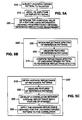
- Such further embodiments of a method according to the present invention are illustrated by flow chart and block flow diagram in FIGS. 5A-5D and described below.
- step 200 an arrangement comprising a patterned layer on a substrate is subjected to radiation.
- step 210 the radiation reflected from the arrangement is measured.
- the numerical value of the feature is determined in step 220 by using information obtained from previously obtained reflectance measurements. Step 220 may be accomplished using a number of methods, two examples of which are described below.
- archived data obtained in steps 300 and 305, is compared, in step 310, with the reflectance spectrum of an uncharacterized pattern.
- the archived data or data base is obtained according to steps 300 and 305 wherein a number of reference patterns are formed and reflectance spectra are then obtained for such reference patterns.
- Features of interest for each reference pattern are measured by SEM or other suitable method.
- the reference reflectance spectra and measured values for features of interest for each reference pattern are organized into a data base or archive by methods known to those skilled in the art.
- a value i.e., the size of a feature of interest, may be determined.
- the numerical value of a feature may be determined by developing a correlation between the feature and reflectance.
- reflectance measurements are obtained for a plurality of reference patterns of known structure.
- the numerical value of a feature of interest is regressed against the reflectance of the reference patterns over the range of suitable wavelengths, as previously described.
- the numerical value of the feature may then be expressed as a function of the reflectance.
- the correlation may be expressed algebraically or graphically.
- the steps discussed in FIGS. 5A-5C may be accomplished by the exemplary arrangement of equipment shown in FIG. 5D.
- the archived data or data base of reference reflectance measurements and measured values of various features of interest, such as the line width of a line and space pattern, may be obtained as follows. Reflectance measurements for a plurality of patterns are first obtained by equipment such as a spectral reflectometer 340 suitable for such purpose. Suitable reflectometers include the Nanometrics 4000 Series or the Prometrix 1050 UV.
- FIG. 5E A simplified block diagram of a spectral reflectometer 340 is shown in FIG. 5E.
- Radiation is provided by an illumination source 342.
- the illumination source 342 is typically a broadband source such as xenon arc lamp. Such a source typically provides radiation ranging in wavelength from about 220 to 800 nm. Illumination source 342 may also include various filters, shutters, a focus aperature and various drive solenoids and stepper motors, not shown in the Figure. Radiation from the illumination source 342 is focussed on a beam splitter 344. One beam, not shown, generated by the beam splitter 344 functions as a reference. This reference beam is guided to the spectrometer assembly 347 for processing.
- the other beam is directed toward a wafer 345 and focused over the pattern to be characterized.
- Reflected radiation 346 is received by the spectrometer assembly 347.
- reflected radiation 346 is typically resolved into its spectral components by a grating.
- Each spectral component of the reflected radiation 346 i.e., radiation of a particular wavelength, is reflected off the grating to a location dictated by that particular wavelength.
- Photodetectors positioned at such locations receive the radiation and generate an electrical signal proportional to the amount of incident radiation.
- a signal generated by a particular photodetector is associated with radiation having a particular wavelength.
- the various signals generated by the activated photodetectors are processed by the processor 348.
- a reflectance spectrum, average reflectance over a wavelength range or other expression of the amount of reflected radiation for a corresponding wavelength may then be calculated.
- the aforementioned discussion of the spectral reflectometer 340 is intended to provide an overview of its operation and some of its important elements. As known to those skilled in the art, the spectral reflectometer 340 typically includes other elements, not shown, for accomplishing various other functions.
- a measurement device 350 is used to directly measure features of the plurality of patterns.
- a scanning electron microscope such as the S7000 by Hitachi, Ltd. is suitable for performing such measurements.
- a suitably programmed microprocessor 360 receives, either directly or indirectly, the reflectance measurements and direct measurement data from the spectral reflectometer 340 and the measurement device 350 and stores such information in memory 370.
- a reflectance measurement as well as values representative of measurements of features of the pattern, are stored in memory 370.
- Such information forms the archive or data base.
- the microprocessor 360 is preferably programmed to regress the reflectance measurement and direct measurment data stored in memory 370 to develop a correlation as discussed above in conjunction with FIG. 5C.
- the arrangement depicted in FIG. 5D may be used determine the numerical value of a feature of an unmeasured pattern as follows.
- a reflectance spectrum may be obtained for an unmeasured pattern using the spectral reflectometer 340.
- Such spectral information is received by the microprocessor 360 which is suitably programmed to compare the reflectance spectrum to the reference reflectance spectra stored in the memory 370. If a match is found between reflectance spectra stored in memory and the reflectance spectra corresponding to the unmeasured pattern, then the reference pattern and the unmeasured pattern are substantially identical.
- Measurement data from memory 370 corresponding to the matching reference pattern is displayed. Thus, the size of a feature of an unmeasured pattern may be determined.
- an average reflectance value rather than a full reflectance spectra, is obtained from the spectral reflectometer 340, then such a value may be used to estimate the size of a feature by applying a previously developed correlation, as discussed above, to the average reflectance value.
- the thickness T and profile angle ⁇ of the lines, such as lines 5a and 5b of FIG. 3A, and the pitch of the pattern should be invariable, the variable being the line width W. If the only variable is the line width W, then differences in the reflectance spectra obtained for different line and space patterns result from differences in the line width W of such patterns. Thus, the line width W of the pattern being measured is equal to the line width of the pattern from which the matching reference reflectance spectra was obtained. Alternatively, line width may be held constant and some other parameter may be varied.
- FIG. 6 shows four reflectance spectra 40, 42, 44 and 46 that were obtained for four arrangements, 40a, 42a, 44a and 46a, respectively, using the Nanometrics 400 Series spectral reflectometer.
- the arrangements, not shown, comprised patterned novalac photoresist on silicon.
- the patterned photoresist of arrangements 40a, 42a, 44a and 46a was patterned into line and space patterns, similar to those shown in FIGS. 1 & 3A.
- the line and space pattern of each of the arrangements 40a - 46a had a 1.0 ⁇ m pitch.
- the thickness and profile angle of the lines and of the four patterns was substantially the same.
- the line width of the lines of the four patterns was different, however, decreasing from a maximum line width in arrangement 40a to a minimum width in arrangement 46a.
- FIG. 7 illustrates such a correlation 60 between line width and reflectance between 220 to 300 nm for such a 1.0 ⁇ m pitch line and space pattern.
- a method in accordance with the present invention may be used for quality control of a lithographic writing process.
- a lithographic writing process may be used to produce a pattern having desired features and feature size.
- a number of parameters affect the ability to produce a pattern having desired features using such a process. For example, the age of photoresist being patterned, the chemical composition of the photoresist developer solution, and, perhaps most importantly, the dose of radiation used to expose the photoresist will all affect the resulting pattern. As such, it is desirable to routinely monitor the pattern being produced.
- test patterns are developed, reflectance measurements are obtained and features of the test patterns are measured by suitable means such as SEM.
- the feature of interest such as the line width of a line and space pattern, may be correlated to reflectance according to the present invention.
- a reference reflectance spectrum is obtained for a pattern having the specific features to be reproduced in the manufacturing process.
- the operating parameters of the writing process are then set to produce a pattern having a specific reflectance, i.e., one which will result in a pattern having a desired feature, such as a 0.5 ⁇ m line width.
- step 430 regular production patterns are periodically sampled, preferably according to statistical methods, and a reflectance measurement is obtained for each sampled pattern. The reflectance measurement for each sampled pattern is then compared, as appropriate, to the reference spectrum or correlation. If the reflectance measurement from a sampled pattern deviates from the reference or correlation, then the pattern being produced is off-specification. Once alerted to off-specification production, the operator of the lithographic writing process may check the various parameters to determine what parameter should be adjusted, as indicated in step 440.
- the photoresist is exposed to radiation, typically UV, through a patterned mask.
- a suitable exemplary photolithographic exposure tool 450 is a stepper, well known to those skilled in the art. Several exemplary steppers are described in U.S. Pat. Nos. 4,616,908, 4,206,494 and 4,425,037.
- the photoresist layer is developed in developer 460. Tetramethyl-ammonium-hydroxide is typically used as a developer fluid.
- the patterned layer which may have the form of a line and space pattern, for example.
- the patterned wafer is next etched in an etcher 500 and then the photoresist remaining on the wafer is removed.
- a pattern such as a line and space pattern, may be etched into the wafer to form a mechanical feature such as a optical diffraction grating.
- wafers may be diverted, after development, from the etcher to a spectral reflectometer 470 wherein a reflectance measurement is obtained.
- spectral information is then received by a microprocessor 480 which is programmed to compare such information to a reference pattern or apply it to a correlation stored in a memory 490.
- a reference pattern or correlation is stored in memory as previously discussed. If a deviation exists between the reflectance measurement from the diverted sample and that of the reference, then an operator is alerted by a visual or audible alarm that off-specification patterns are being produced and that the operation should be checked and adjusted as appropriate.
- the method of the present invention may be used to quantify features other than the line width of a line and space pattern.
- the embodiments discussed herein are directed to applications wherein the substrate is generally more reflective than the patterned layer
- the contemplated scope of the present invention includes arrangements wherein the patterned layer is generally more reflective than the substrate and wherein the arrangement is irradiated by radiation having a suitable range of wavelengths such that the patterned material reflects more radiation than the substrate, and the substrate absorbs more radiation than the patterned material.
Landscapes
- Physics & Mathematics (AREA)
- General Physics & Mathematics (AREA)
- Exposure And Positioning Against Photoresist Photosensitive Materials (AREA)
- Photosensitive Polymer And Photoresist Processing (AREA)
- Investigating Or Analysing Materials By Optical Means (AREA)
- Exposure Of Semiconductors, Excluding Electron Or Ion Beam Exposure (AREA)
Applications Claiming Priority (2)
| Application Number | Priority Date | Filing Date | Title |
|---|---|---|---|
| US388934 | 1995-02-15 | ||
| US08/388,934 US5607800A (en) | 1995-02-15 | 1995-02-15 | Method and arrangement for characterizing micro-size patterns |
Publications (1)
| Publication Number | Publication Date |
|---|---|
| EP0727715A1 true EP0727715A1 (de) | 1996-08-21 |
Family
ID=23536144
Family Applications (1)
| Application Number | Title | Priority Date | Filing Date |
|---|---|---|---|
| EP96300825A Withdrawn EP0727715A1 (de) | 1995-02-15 | 1996-02-07 | Verfahren und Anordnung zur Charakterisierung von Mikromustern |
Country Status (4)
| Country | Link |
|---|---|
| US (1) | US5607800A (de) |
| EP (1) | EP0727715A1 (de) |
| JP (1) | JPH08255751A (de) |
| KR (1) | KR960032584A (de) |
Cited By (22)
| Publication number | Priority date | Publication date | Assignee | Title |
|---|---|---|---|---|
| EP1065567A3 (de) * | 1999-06-29 | 2001-05-16 | Applied Materials, Inc. | Integrierte Kontrolle einer kritischen Dimension |
| EP0973068A3 (de) * | 1998-07-14 | 2001-05-30 | Nova Measuring Instruments Limited | Methode und System zur Steuerung eines photolithographischen Verfahrens |
| US6424417B1 (en) | 1998-06-14 | 2002-07-23 | Nova Measuring Instruments Ltd. | Method and system for controlling the photolithography process |
| WO2002080264A3 (en) * | 2001-03-29 | 2003-01-09 | Advanced Micro Devices Inc | Method and apparatus for controlling feature critical dimensions based on scatterometry derived profile |
| US6625497B2 (en) | 2000-11-20 | 2003-09-23 | Applied Materials Inc. | Semiconductor processing module with integrated feedback/feed forward metrology |
| WO2003081662A1 (en) * | 2002-03-19 | 2003-10-02 | Advanced Micro Devices, Inc. | Method and structure for calibrating scatterometry-based metrology tool used to measure dimensions of features on a semiconductor device |
| WO2003074995A3 (en) * | 2002-02-28 | 2004-01-08 | Advanced Micro Devices Inc | Method of using high yielding spectra scatterometry measurements to control semiconductor manufacturing processes and systems for accomplishing same |
| US6858361B2 (en) | 2002-03-01 | 2005-02-22 | David S. L. Mui | Methodology for repeatable post etch CD in a production tool |
| US6911399B2 (en) | 2003-09-19 | 2005-06-28 | Applied Materials, Inc. | Method of controlling critical dimension microloading of photoresist trimming process by selective sidewall polymer deposition |
| WO2005038529A3 (en) * | 2003-10-20 | 2005-07-07 | Koninkl Philips Electronics Nv | Method for determining relative swing curve amplitude |
| US6924088B2 (en) | 2002-06-20 | 2005-08-02 | Applied Materials, Inc. | Method and system for realtime CD microloading control |
| US6960416B2 (en) | 2002-03-01 | 2005-11-01 | Applied Materials, Inc. | Method and apparatus for controlling etch processes during fabrication of semiconductor devices |
| WO2005041291A3 (en) * | 2003-10-15 | 2005-12-29 | Infineon Technologies Ag | Mask and method for using the mask in lithographic processing |
| EP1483355A4 (de) * | 2002-02-12 | 2007-05-16 | Timbre Tech Inc | Profilverfeinerung für messtechnik der integrierten schaltkreise |
| US7225047B2 (en) | 2002-03-19 | 2007-05-29 | Applied Materials, Inc. | Method, system and medium for controlling semiconductor wafer processes using critical dimension measurements |
| US7265382B2 (en) | 2002-11-12 | 2007-09-04 | Applied Materials, Inc. | Method and apparatus employing integrated metrology for improved dielectric etch efficiency |
| EP1591751A3 (de) * | 2004-03-31 | 2008-08-20 | NEC Electronics Corporation | Verfahren und Vorrichtung zur Messung von Mikrostrukturen sowie Mikrostrukturanalysesystem |
| US7601272B2 (en) | 2005-01-08 | 2009-10-13 | Applied Materials, Inc. | Method and apparatus for integrating metrology with etch processing |
| US7626711B2 (en) | 1999-07-09 | 2009-12-01 | Nova Measuring Instruments | Method and system for measuring patterned structures |
| US7846848B2 (en) | 2005-01-08 | 2010-12-07 | Applied Materials, Inc. | Cluster tool with integrated metrology chamber for transparent substrates |
| US8531678B2 (en) | 1999-07-09 | 2013-09-10 | Nova Measuring Instruments, Ltd. | Method and system for measuring patterned structures |
| CN110462523A (zh) * | 2017-03-23 | 2019-11-15 | Asml荷兰有限公司 | 结构的不对称性监视 |
Families Citing this family (79)
| Publication number | Priority date | Publication date | Assignee | Title |
|---|---|---|---|---|
| US5825498A (en) * | 1996-02-05 | 1998-10-20 | Micron Technology, Inc. | Ultraviolet light reflectance method for evaluating the surface characteristics of opaque materials |
| US6195163B1 (en) | 1996-02-05 | 2001-02-27 | Micron Technology, Inc. | Reflectance method for evaluating the surface characteristics of opaque materials |
| JP2856711B2 (ja) * | 1996-07-16 | 1999-02-10 | 山形日本電気株式会社 | 位置検出方法 |
| US5987160A (en) * | 1997-04-02 | 1999-11-16 | Delco Electronics Corporation | Method and apparatus for inspecting a photoresist material by inducing and detecting fluorescence of the photoresist material |
| US6483580B1 (en) * | 1998-03-06 | 2002-11-19 | Kla-Tencor Technologies Corporation | Spectroscopic scatterometer system |
| US20020030813A1 (en) * | 1999-03-29 | 2002-03-14 | Norton Adam E. | Spectroscopic measurement system using an off-axis spherical mirror and refractive elements |
| US6184984B1 (en) | 1999-02-09 | 2001-02-06 | Kla-Tencor Corporation | System for measuring polarimetric spectrum and other properties of a sample |
| US6326618B1 (en) | 1999-07-02 | 2001-12-04 | Agere Systems Guardian Corp. | Method of analyzing semiconductor surface with patterned feature using line width metrology |
| US6358860B1 (en) * | 1999-10-07 | 2002-03-19 | Vlsi Standards, Inc. | Line width calibration standard manufacturing and certifying method |
| US6327035B1 (en) * | 1999-11-30 | 2001-12-04 | Nsh Technology, Inc. | Method and apparatus for optically examining miniature patterns |
| KR100513574B1 (ko) * | 2000-01-26 | 2005-09-09 | 팀버 테크놀로지스, 인코포레이티드 | 신속 정밀한 결합-파 분석을 위한 층 내부의 계산들의 캐싱 |
| US6472238B1 (en) * | 2000-02-09 | 2002-10-29 | Therma-Wave, Inc. | Evaluation of etching processes in semiconductors |
| AU2001279247A1 (en) | 2000-08-10 | 2002-02-25 | Sensys Instruments Corporation | Database interpolation method for optical measurement of diffractive microstructures |
| US7115858B1 (en) | 2000-09-25 | 2006-10-03 | Nanometrics Incorporated | Apparatus and method for the measurement of diffracting structures |
| US7099005B1 (en) * | 2000-09-27 | 2006-08-29 | Kla-Tencor Technologies Corporation | System for scatterometric measurements and applications |
| IL140179A (en) * | 2000-12-07 | 2004-09-27 | Nova Measuring Instr Ltd | Method and system for measuring in patterned structures |
| US6721052B2 (en) * | 2000-12-20 | 2004-04-13 | Kla-Technologies Corporation | Systems for measuring periodic structures |
| US6898537B1 (en) | 2001-04-27 | 2005-05-24 | Nanometrics Incorporated | Measurement of diffracting structures using one-half of the non-zero diffracted orders |
| US7382447B2 (en) * | 2001-06-26 | 2008-06-03 | Kla-Tencor Technologies Corporation | Method for determining lithographic focus and exposure |
| US6713753B1 (en) | 2001-07-03 | 2004-03-30 | Nanometrics Incorporated | Combination of normal and oblique incidence polarimetry for the characterization of gratings |
| US6704661B1 (en) * | 2001-07-16 | 2004-03-09 | Therma-Wave, Inc. | Real time analysis of periodic structures on semiconductors |
| US7061615B1 (en) | 2001-09-20 | 2006-06-13 | Nanometrics Incorporated | Spectroscopically measured overlay target |
| US6819427B1 (en) * | 2001-10-10 | 2004-11-16 | Advanced Micro Devices, Inc. | Apparatus of monitoring and optimizing the development of a photoresist material |
| US6898596B2 (en) * | 2001-10-23 | 2005-05-24 | Therma-Wave, Inc. | Evolution of library data sets |
| JP3817464B2 (ja) * | 2001-11-13 | 2006-09-06 | 株式会社日立ハイテクノロジーズ | 微細パターンの3次元形状測定システム、及び3次元形状測定方法 |
| US6894790B2 (en) * | 2001-11-13 | 2005-05-17 | Hitachi High-Technologies Corporation | Micropattern shape measuring system and method |
| TW569368B (en) * | 2001-11-14 | 2004-01-01 | Tokyo Electron Ltd | Substrate inspecting apparatus, coating and developing apparatus, and substrate inspecting method |
| US6809824B1 (en) * | 2001-11-30 | 2004-10-26 | Lsi Logic Corporation | Alignment process for integrated circuit structures on semiconductor substrate using scatterometry measurements of latent images in spaced apart test fields on substrate |
| US6608690B2 (en) * | 2001-12-04 | 2003-08-19 | Timbre Technologies, Inc. | Optical profilometry of additional-material deviations in a periodic grating |
| WO2003054475A2 (en) * | 2001-12-19 | 2003-07-03 | Kla-Tencor Technologies Corporation | Parametric profiling using optical spectroscopic systems |
| US6982791B2 (en) * | 2001-12-19 | 2006-01-03 | Therma-Wave, Inc. | Scatterometry to simultaneously measure critical dimensions and film properties |
| US6982793B1 (en) | 2002-04-04 | 2006-01-03 | Nanometrics Incorporated | Method and apparatus for using an alignment target with designed in offset |
| US6949462B1 (en) | 2002-04-04 | 2005-09-27 | Nanometrics Incorporated | Measuring an alignment target with multiple polarization states |
| US6947135B2 (en) * | 2002-07-01 | 2005-09-20 | Therma-Wave, Inc. | Reduced multicubic database interpolation method for optical measurement of diffractive microstructures |
| US6919964B2 (en) * | 2002-07-09 | 2005-07-19 | Therma-Wave, Inc. | CD metrology analysis using a finite difference method |
| US6992764B1 (en) | 2002-09-30 | 2006-01-31 | Nanometrics Incorporated | Measuring an alignment target with a single polarization state |
| US6950190B2 (en) * | 2003-01-09 | 2005-09-27 | Therma-Wave, Inc. | Scatterometry for junction metrology |
| US7126131B2 (en) * | 2003-01-16 | 2006-10-24 | Metrosol, Inc. | Broad band referencing reflectometer |
| US7067818B2 (en) * | 2003-01-16 | 2006-06-27 | Metrosol, Inc. | Vacuum ultraviolet reflectometer system and method |
| US7394551B2 (en) * | 2003-01-16 | 2008-07-01 | Metrosol, Inc. | Vacuum ultraviolet referencing reflectometer |
| US20080246951A1 (en) * | 2007-04-09 | 2008-10-09 | Phillip Walsh | Method and system for using reflectometry below deep ultra-violet (DUV) wavelengths for measuring properties of diffracting or scattering structures on substrate work-pieces |
| US8564780B2 (en) * | 2003-01-16 | 2013-10-22 | Jordan Valley Semiconductors Ltd. | Method and system for using reflectometry below deep ultra-violet (DUV) wavelengths for measuring properties of diffracting or scattering structures on substrate work pieces |
| US7026626B2 (en) * | 2003-01-16 | 2006-04-11 | Metrosol, Inc. | Semiconductor processing techniques utilizing vacuum ultraviolet reflectometer |
| US7352453B2 (en) * | 2003-01-17 | 2008-04-01 | Kla-Tencor Technologies Corporation | Method for process optimization and control by comparison between 2 or more measured scatterometry signals |
| US7069153B2 (en) * | 2003-01-28 | 2006-06-27 | Therma-Wave, Inc. | CD metrology method |
| US6888632B2 (en) * | 2003-02-28 | 2005-05-03 | Therma-Wave, Inc. | Modulated scatterometry |
| US7233390B2 (en) * | 2003-03-31 | 2007-06-19 | Therma-Wave, Inc. | Scatterometry for samples with non-uniform edges |
| US7145664B2 (en) * | 2003-04-18 | 2006-12-05 | Therma-Wave, Inc. | Global shape definition method for scatterometry |
| US6891628B2 (en) * | 2003-06-25 | 2005-05-10 | N & K Technology, Inc. | Method and apparatus for examining features on semi-transparent and transparent substrates |
| US7271921B2 (en) * | 2003-07-23 | 2007-09-18 | Kla-Tencor Technologies Corporation | Method and apparatus for determining surface layer thickness using continuous multi-wavelength surface scanning |
| US7145654B2 (en) * | 2003-10-01 | 2006-12-05 | Tokyo Electron Limited | Method and apparatus to reduce spotsize in an optical metrology instrument |
| US7126700B2 (en) * | 2003-12-12 | 2006-10-24 | Timbre Technologies, Inc. | Parametric optimization of optical metrology model |
| US7248364B2 (en) * | 2003-12-19 | 2007-07-24 | N&K Technology, Inc. | Apparatus and method for optical characterization of a sample over a broadband of wavelengths with a small spot size |
| US7327457B2 (en) * | 2003-12-19 | 2008-02-05 | N&K Technology, Inc. | Apparatus and method for optical characterization of a sample over a broadband of wavelengths while minimizing polarization changes |
| US7304735B2 (en) * | 2004-04-02 | 2007-12-04 | Kla-Tencor Technologies | Broadband wavelength selective filter |
| US7212293B1 (en) * | 2004-06-01 | 2007-05-01 | N&K Technology, Inc. | Optical determination of pattern feature parameters using a scalar model having effective optical properties |
| US7399975B2 (en) * | 2004-08-11 | 2008-07-15 | Metrosol, Inc. | Method and apparatus for performing highly accurate thin film measurements |
| US7804059B2 (en) * | 2004-08-11 | 2010-09-28 | Jordan Valley Semiconductors Ltd. | Method and apparatus for accurate calibration of VUV reflectometer |
| US7511265B2 (en) * | 2004-08-11 | 2009-03-31 | Metrosol, Inc. | Method and apparatus for accurate calibration of a reflectometer by using a relative reflectance measurement |
| US7282703B2 (en) * | 2004-08-11 | 2007-10-16 | Metrosol, Inc. | Method and apparatus for accurate calibration of a reflectometer by using a relative reflectance measurement |
| US7663097B2 (en) * | 2004-08-11 | 2010-02-16 | Metrosol, Inc. | Method and apparatus for accurate calibration of a reflectometer by using a relative reflectance measurement |
| KR100625168B1 (ko) * | 2004-08-23 | 2006-09-20 | 삼성전자주식회사 | 기판에 형성된 패턴의 검사방법 및 이를 수행하기 위한검사장치 |
| US8401637B2 (en) * | 2004-11-24 | 2013-03-19 | Galvani, Ltd. | Medium voltage therapy applications in treating cardiac arrest |
| US7515253B2 (en) * | 2005-01-12 | 2009-04-07 | Kla-Tencor Technologies Corporation | System for measuring a sample with a layer containing a periodic diffracting structure |
| US7747424B2 (en) * | 2006-03-17 | 2010-06-29 | Kla-Tencor Corporation | Scatterometry multi-structure shape definition with multi-periodicity |
| US7643666B2 (en) * | 2006-08-08 | 2010-01-05 | Asml Netherlands B.V. | Method and apparatus for angular-resolved spectroscopic lithography characterization |
| US20080129986A1 (en) * | 2006-11-30 | 2008-06-05 | Phillip Walsh | Method and apparatus for optically measuring periodic structures using orthogonal azimuthal sample orientations |
| US7777184B2 (en) * | 2007-08-30 | 2010-08-17 | Taiwan Semiconductor Manufacturing Company, Ltd. | Method for photoresist characterization and analysis |
| US20090219537A1 (en) * | 2008-02-28 | 2009-09-03 | Phillip Walsh | Method and apparatus for using multiple relative reflectance measurements to determine properties of a sample using vacuum ultra violet wavelengths |
| US8090558B1 (en) | 2008-06-09 | 2012-01-03 | Kla-Tencor Corporation | Optical parametric model optimization |
| US8153987B2 (en) * | 2009-05-22 | 2012-04-10 | Jordan Valley Semiconductors Ltd. | Automated calibration methodology for VUV metrology system |
| US8867041B2 (en) | 2011-01-18 | 2014-10-21 | Jordan Valley Semiconductor Ltd | Optical vacuum ultra-violet wavelength nanoimprint metrology |
| US8565379B2 (en) | 2011-03-14 | 2013-10-22 | Jordan Valley Semiconductors Ltd. | Combining X-ray and VUV analysis of thin film layers |
| US8468471B2 (en) | 2011-09-23 | 2013-06-18 | Kla-Tencor Corp. | Process aware metrology |
| US9311431B2 (en) * | 2011-11-03 | 2016-04-12 | Kla-Tencor Corporation | Secondary target design for optical measurements |
| US10429320B2 (en) | 2013-06-04 | 2019-10-01 | Kla-Tencor Corporation | Method for auto-learning tool matching |
| NL2020776A (en) * | 2017-05-04 | 2018-11-09 | Asml Holding Nv | Method, substrate and apparatus to measure performance of optical metrology |
| EP3951500A1 (de) * | 2020-08-05 | 2022-02-09 | ASML Netherlands B.V. | Verfahren zur bestimmung der abweichung eines herstellungsverfahrens, kalibrierungsverfahren, prüfwerkzeug, herstellungssystem und muster |
| KR20230044204A (ko) | 2020-08-05 | 2023-04-03 | 에이에스엠엘 네델란즈 비.브이. | 제조 공정 편차 결정 방법, 교정 방법, 검사 도구, 제조 시스템 및 샘플 |
Citations (1)
| Publication number | Priority date | Publication date | Assignee | Title |
|---|---|---|---|---|
| US4757207A (en) * | 1987-03-03 | 1988-07-12 | International Business Machines Corporation | Measurement of registration of overlaid test patterns by the use of reflected light |
Family Cites Families (5)
| Publication number | Priority date | Publication date | Assignee | Title |
|---|---|---|---|---|
| KR930005569B1 (ko) * | 1987-10-02 | 1993-06-23 | 도오교오 에레구토론 가부시끼가이샤 | 패턴 인식 방법 |
| US5101111A (en) * | 1989-07-13 | 1992-03-31 | Dainippon Screen Mfg. Co., Ltd. | Method of measuring thickness of film with a reference sample having a known reflectance |
| US5184021A (en) * | 1991-06-24 | 1993-02-02 | Siscan Systems, Inc. | Method and apparatus for measuring the dimensions of patterned features on a lithographic photomask |
| US5320864A (en) * | 1992-06-29 | 1994-06-14 | Lsi Logic Corporation | Sedimentary deposition of photoresist on semiconductor wafers |
| US5363171A (en) * | 1993-07-29 | 1994-11-08 | The United States Of America As Represented By The Director, National Security Agency | Photolithography exposure tool and method for in situ photoresist measurments and exposure control |
-
1995
- 1995-02-15 US US08/388,934 patent/US5607800A/en not_active Expired - Lifetime
-
1996
- 1996-02-07 EP EP96300825A patent/EP0727715A1/de not_active Withdrawn
- 1996-02-14 KR KR1019960003513A patent/KR960032584A/ko not_active Abandoned
- 1996-02-15 JP JP8027567A patent/JPH08255751A/ja not_active Withdrawn
Patent Citations (1)
| Publication number | Priority date | Publication date | Assignee | Title |
|---|---|---|---|---|
| US4757207A (en) * | 1987-03-03 | 1988-07-12 | International Business Machines Corporation | Measurement of registration of overlaid test patterns by the use of reflected light |
Non-Patent Citations (2)
| Title |
|---|
| ANONYMOUS: "Phase-Sensitive Overlay Analysis Spectrometry.", IBM TECHNICAL DISCLOSURE BULLETIN, vol. 32, no. 10A, March 1990 (1990-03-01), NEW YORK, US, pages 170 - 174, XP002003938 * |
| ANONYMOUS: "Spectroscopic Pitch Measurement Technique", IBM TECHNICAL DISCLOSURE BULLETIN, vol. 32, no. 4B, September 1989 (1989-09-01), NEW YORK, US, pages 391 - 392, XP002003937 * |
Cited By (42)
| Publication number | Priority date | Publication date | Assignee | Title |
|---|---|---|---|---|
| US6424417B1 (en) | 1998-06-14 | 2002-07-23 | Nova Measuring Instruments Ltd. | Method and system for controlling the photolithography process |
| EP0973068A3 (de) * | 1998-07-14 | 2001-05-30 | Nova Measuring Instruments Limited | Methode und System zur Steuerung eines photolithographischen Verfahrens |
| EP1065567A3 (de) * | 1999-06-29 | 2001-05-16 | Applied Materials, Inc. | Integrierte Kontrolle einer kritischen Dimension |
| US6388253B1 (en) | 1999-06-29 | 2002-05-14 | Applied Materials, Inc. | Integrated critical dimension control for semiconductor device manufacturing |
| US6486492B1 (en) | 1999-06-29 | 2002-11-26 | Applied Materials, Inc. | Integrated critical dimension control for semiconductor device manufacturing |
| US8531678B2 (en) | 1999-07-09 | 2013-09-10 | Nova Measuring Instruments, Ltd. | Method and system for measuring patterned structures |
| US9184102B2 (en) | 1999-07-09 | 2015-11-10 | Nova Measuring Instruments Ltd. | Method and system for measuring patterned structures |
| US8023122B2 (en) | 1999-07-09 | 2011-09-20 | Nova Measuring Instruments Ltd. | Method and system for measuring patterned structures |
| US7864344B1 (en) | 1999-07-09 | 2011-01-04 | Nova Measuring Instruments Ltd. | Method and system for measuring patterned structures |
| US7864343B2 (en) | 1999-07-09 | 2011-01-04 | Nova Measuring Instruments Ltd. | Method and system for measuring patterned structures |
| US7791740B2 (en) | 1999-07-09 | 2010-09-07 | Nova Measuring Instruments Ltd. | Method and system for measuring patterned structures |
| US7760368B2 (en) | 1999-07-09 | 2010-07-20 | Nova Measuring Instruments Ltd. | Method and system for measuring patterned structures |
| US7663768B2 (en) | 1999-07-09 | 2010-02-16 | Nova Measuring Instruments Ltd. | Method and system for measuring patterned structures |
| US7626711B2 (en) | 1999-07-09 | 2009-12-01 | Nova Measuring Instruments | Method and system for measuring patterned structures |
| US6625497B2 (en) | 2000-11-20 | 2003-09-23 | Applied Materials Inc. | Semiconductor processing module with integrated feedback/feed forward metrology |
| WO2002080264A3 (en) * | 2001-03-29 | 2003-01-09 | Advanced Micro Devices Inc | Method and apparatus for controlling feature critical dimensions based on scatterometry derived profile |
| EP1483355A4 (de) * | 2002-02-12 | 2007-05-16 | Timbre Tech Inc | Profilverfeinerung für messtechnik der integrierten schaltkreise |
| US6785009B1 (en) | 2002-02-28 | 2004-08-31 | Advanced Micro Devices, Inc. | Method of using high yielding spectra scatterometry measurements to control semiconductor manufacturing processes, and systems for accomplishing same |
| KR101018837B1 (ko) * | 2002-02-28 | 2011-03-04 | 어드밴스드 마이크로 디바이시즈, 인코포레이티드 | 반도체 제조 공정을 제어하기 위한 고수율의 분광 스케테로메트리측정을 사용하는 방법과 이를 구현하는 시스템 |
| GB2405201A (en) * | 2002-02-28 | 2005-02-23 | Advanced Micro Devices Inc | Method of using high yielding spectra scatterometry measurements to control semiconductor manufacturing processes and systems for accomplishing same |
| GB2405201B (en) * | 2002-02-28 | 2005-09-14 | Advanced Micro Devices Inc | Method of using high yielding spectra scatterometry measurements to control semiconductor manufacturing processes and systems for accomplishing same |
| WO2003074995A3 (en) * | 2002-02-28 | 2004-01-08 | Advanced Micro Devices Inc | Method of using high yielding spectra scatterometry measurements to control semiconductor manufacturing processes and systems for accomplishing same |
| US6960416B2 (en) | 2002-03-01 | 2005-11-01 | Applied Materials, Inc. | Method and apparatus for controlling etch processes during fabrication of semiconductor devices |
| US7498106B2 (en) | 2002-03-01 | 2009-03-03 | Applied Materials, Inc. | Method and apparatus for controlling etch processes during fabrication of semiconductor devices |
| US6858361B2 (en) | 2002-03-01 | 2005-02-22 | David S. L. Mui | Methodology for repeatable post etch CD in a production tool |
| WO2003081662A1 (en) * | 2002-03-19 | 2003-10-02 | Advanced Micro Devices, Inc. | Method and structure for calibrating scatterometry-based metrology tool used to measure dimensions of features on a semiconductor device |
| US7225047B2 (en) | 2002-03-19 | 2007-05-29 | Applied Materials, Inc. | Method, system and medium for controlling semiconductor wafer processes using critical dimension measurements |
| US6742168B1 (en) | 2002-03-19 | 2004-05-25 | Advanced Micro Devices, Inc. | Method and structure for calibrating scatterometry-based metrology tool used to measure dimensions of features on a semiconductor device |
| GB2406215A (en) * | 2002-03-19 | 2005-03-23 | Advanced Micro Devices Inc | Method and structure for calibrating scatterometry-based metrology tool used to measure dimensions of features on a semiconductor device |
| GB2406215B (en) * | 2002-03-19 | 2005-12-21 | Advanced Micro Devices Inc | Method and apparatus for calibrating scatterometry-based metrology tool used to measure dimensions of features on a semiconductor device |
| US6924088B2 (en) | 2002-06-20 | 2005-08-02 | Applied Materials, Inc. | Method and system for realtime CD microloading control |
| US7265382B2 (en) | 2002-11-12 | 2007-09-04 | Applied Materials, Inc. | Method and apparatus employing integrated metrology for improved dielectric etch efficiency |
| US6911399B2 (en) | 2003-09-19 | 2005-06-28 | Applied Materials, Inc. | Method of controlling critical dimension microloading of photoresist trimming process by selective sidewall polymer deposition |
| US7030506B2 (en) | 2003-10-15 | 2006-04-18 | Infineon Technologies, Ag | Mask and method for using the mask in lithographic processing |
| WO2005041291A3 (en) * | 2003-10-15 | 2005-12-29 | Infineon Technologies Ag | Mask and method for using the mask in lithographic processing |
| WO2005038529A3 (en) * | 2003-10-20 | 2005-07-07 | Koninkl Philips Electronics Nv | Method for determining relative swing curve amplitude |
| US7580134B2 (en) | 2004-03-31 | 2009-08-25 | Nec Electronics Corporation | Method of measuring micro-structure, micro-structure measurement apparatus, and micro-structure analytical system |
| EP1591751A3 (de) * | 2004-03-31 | 2008-08-20 | NEC Electronics Corporation | Verfahren und Vorrichtung zur Messung von Mikrostrukturen sowie Mikrostrukturanalysesystem |
| US7846848B2 (en) | 2005-01-08 | 2010-12-07 | Applied Materials, Inc. | Cluster tool with integrated metrology chamber for transparent substrates |
| US7601272B2 (en) | 2005-01-08 | 2009-10-13 | Applied Materials, Inc. | Method and apparatus for integrating metrology with etch processing |
| CN110462523A (zh) * | 2017-03-23 | 2019-11-15 | Asml荷兰有限公司 | 结构的不对称性监视 |
| CN110462523B (zh) * | 2017-03-23 | 2022-02-11 | Asml荷兰有限公司 | 结构的不对称性监视 |
Also Published As
| Publication number | Publication date |
|---|---|
| KR960032584A (ko) | 1996-09-17 |
| US5607800A (en) | 1997-03-04 |
| JPH08255751A (ja) | 1996-10-01 |
Similar Documents
| Publication | Publication Date | Title |
|---|---|---|
| US5607800A (en) | Method and arrangement for characterizing micro-size patterns | |
| US6327035B1 (en) | Method and apparatus for optically examining miniature patterns | |
| KR100543534B1 (ko) | 검사방법 및 디바이스제조방법 | |
| US5363171A (en) | Photolithography exposure tool and method for in situ photoresist measurments and exposure control | |
| KR100919000B1 (ko) | 검사 방법 및 장치, 리소그래피 장치, 리소그래피 처리 셀및 디바이스 제조방법 | |
| KR100985179B1 (ko) | 검사 방법 및 장치, 리소그래피 장치, 리소그래피 처리 셀및 디바이스 제조 방법 | |
| JP5016579B2 (ja) | モデルの自由及び固定パラメータの選択を支援する方法、特性を測定する方法、デバイス製造方法、分光計及びリソグラフィ装置 | |
| US5674652A (en) | Diffracted light from latent images in photoresist for exposure control | |
| US20100277706A1 (en) | Method of Measurement, an Inspection Apparatus and a Lithographic Apparatus | |
| US4308586A (en) | Method for the precise determination of photoresist exposure time | |
| KR20030040446A (ko) | 회절 시그네춰 분석을 통한 초점 중심 측정방법 | |
| JP2002311564A (ja) | 散乱測定を用いてマスクルールを求めるための方法および装置 | |
| US20030197872A1 (en) | Scatterometric measurement of undercut multi-layer diffracting signatures | |
| JP2004200680A (ja) | 検査方法およびデバイス製造方法 | |
| JP4828499B2 (ja) | 検査方法および装置、リソグラフィ装置、リソグラフィ処理セルおよびデバイス製造方法 | |
| JP2009081436A (ja) | オーバレイエラーの測定方法、検査装置及びリソグラフィ装置 | |
| US9304077B2 (en) | Inspection apparatus and method | |
| JP4142552B2 (ja) | 形状プロファイル測定装置およびそれを用いた半導体デバイスの製造方法 | |
| US5830611A (en) | Use of diffracted light from latent images in photoresist for optimizing image contrast | |
| EP0134453B1 (de) | Verfahren zur Belichtungsberechnung für photolithographische Projektionskopierer | |
| US6891628B2 (en) | Method and apparatus for examining features on semi-transparent and transparent substrates | |
| EP0985977A1 (de) | Analyse von latenten Bildern bei der Herstellung von integrierten Schaltkreisen | |
| US8685626B2 (en) | Method of measuring a characteristic | |
| Toyoshima et al. | Complementary use of scatterometry and SEM for photoresist profile and CD determination | |
| WO2003089888A2 (en) | Scatterometric measurement of undercut multi-layer diffracting structures |
Legal Events
| Date | Code | Title | Description |
|---|---|---|---|
| PUAI | Public reference made under article 153(3) epc to a published international application that has entered the european phase |
Free format text: ORIGINAL CODE: 0009012 |
|
| AK | Designated contracting states |
Kind code of ref document: A1 Designated state(s): DE ES FR GB |
|
| 17P | Request for examination filed |
Effective date: 19970131 |
|
| STAA | Information on the status of an ep patent application or granted ep patent |
Free format text: STATUS: THE APPLICATION HAS BEEN WITHDRAWN |
|
| 18W | Application withdrawn |
Withdrawal date: 19971206 |