EP0728716A1 - Dielektrische Keramik - Google Patents
Dielektrische Keramik Download PDFInfo
- Publication number
- EP0728716A1 EP0728716A1 EP96102686A EP96102686A EP0728716A1 EP 0728716 A1 EP0728716 A1 EP 0728716A1 EP 96102686 A EP96102686 A EP 96102686A EP 96102686 A EP96102686 A EP 96102686A EP 0728716 A1 EP0728716 A1 EP 0728716A1
- Authority
- EP
- European Patent Office
- Prior art keywords
- dielectric
- board
- mol
- dielectric ceramic
- different
- Prior art date
- Legal status (The legal status is an assumption and is not a legal conclusion. Google has not performed a legal analysis and makes no representation as to the accuracy of the status listed.)
- Withdrawn
Links
Images


Classifications
-
- C—CHEMISTRY; METALLURGY
- C04—CEMENTS; CONCRETE; ARTIFICIAL STONE; CERAMICS; REFRACTORIES
- C04B—LIME, MAGNESIA; SLAG; CEMENTS; COMPOSITIONS THEREOF, e.g. MORTARS, CONCRETE OR LIKE BUILDING MATERIALS; ARTIFICIAL STONE; CERAMICS; REFRACTORIES; TREATMENT OF NATURAL STONE
- C04B35/00—Shaped ceramic products characterised by their composition; Ceramics compositions; Processing powders of inorganic compounds preparatory to the manufacturing of ceramic products
- C04B35/01—Shaped ceramic products characterised by their composition; Ceramics compositions; Processing powders of inorganic compounds preparatory to the manufacturing of ceramic products based on oxide ceramics
- C04B35/46—Shaped ceramic products characterised by their composition; Ceramics compositions; Processing powders of inorganic compounds preparatory to the manufacturing of ceramic products based on oxide ceramics based on titanium oxides or titanates
- C04B35/462—Shaped ceramic products characterised by their composition; Ceramics compositions; Processing powders of inorganic compounds preparatory to the manufacturing of ceramic products based on oxide ceramics based on titanium oxides or titanates based on titanates
- C04B35/465—Shaped ceramic products characterised by their composition; Ceramics compositions; Processing powders of inorganic compounds preparatory to the manufacturing of ceramic products based on oxide ceramics based on titanium oxides or titanates based on titanates based on alkaline earth metal titanates
-
- C—CHEMISTRY; METALLURGY
- C04—CEMENTS; CONCRETE; ARTIFICIAL STONE; CERAMICS; REFRACTORIES
- C04B—LIME, MAGNESIA; SLAG; CEMENTS; COMPOSITIONS THEREOF, e.g. MORTARS, CONCRETE OR LIKE BUILDING MATERIALS; ARTIFICIAL STONE; CERAMICS; REFRACTORIES; TREATMENT OF NATURAL STONE
- C04B35/00—Shaped ceramic products characterised by their composition; Ceramics compositions; Processing powders of inorganic compounds preparatory to the manufacturing of ceramic products
- C04B35/01—Shaped ceramic products characterised by their composition; Ceramics compositions; Processing powders of inorganic compounds preparatory to the manufacturing of ceramic products based on oxide ceramics
- C04B35/16—Shaped ceramic products characterised by their composition; Ceramics compositions; Processing powders of inorganic compounds preparatory to the manufacturing of ceramic products based on oxide ceramics based on silicates other than clay
- C04B35/20—Shaped ceramic products characterised by their composition; Ceramics compositions; Processing powders of inorganic compounds preparatory to the manufacturing of ceramic products based on oxide ceramics based on silicates other than clay rich in magnesium oxide, e.g. forsterite
-
- H—ELECTRICITY
- H01—ELECTRIC ELEMENTS
- H01B—CABLES; CONDUCTORS; INSULATORS; SELECTION OF MATERIALS FOR THEIR CONDUCTIVE, INSULATING OR DIELECTRIC PROPERTIES
- H01B3/00—Insulators or insulating bodies characterised by the insulating materials; Selection of materials for their insulating or dielectric properties
- H01B3/02—Insulators or insulating bodies characterised by the insulating materials; Selection of materials for their insulating or dielectric properties mainly consisting of inorganic substances
- H01B3/12—Insulators or insulating bodies characterised by the insulating materials; Selection of materials for their insulating or dielectric properties mainly consisting of inorganic substances ceramics
-
- H—ELECTRICITY
- H01—ELECTRIC ELEMENTS
- H01G—CAPACITORS; CAPACITORS, RECTIFIERS, DETECTORS, SWITCHING DEVICES, LIGHT-SENSITIVE OR TEMPERATURE-SENSITIVE DEVICES OF THE ELECTROLYTIC TYPE
- H01G4/00—Fixed capacitors; Processes of their manufacture
- H01G4/002—Details
- H01G4/018—Dielectrics
- H01G4/06—Solid dielectrics
- H01G4/08—Inorganic dielectrics
- H01G4/12—Ceramic dielectrics
- H01G4/1209—Ceramic dielectrics characterised by the ceramic dielectric material
-
- H—ELECTRICITY
- H10—SEMICONDUCTOR DEVICES; ELECTRIC SOLID-STATE DEVICES NOT OTHERWISE PROVIDED FOR
- H10W—GENERIC PACKAGES, INTERCONNECTIONS, CONNECTORS OR OTHER CONSTRUCTIONAL DETAILS OF DEVICES COVERED BY CLASS H10
- H10W70/00—Package substrates; Interposers; Redistribution layers [RDL]
- H10W70/60—Insulating or insulated package substrates; Interposers; Redistribution layers
- H10W70/67—Insulating or insulated package substrates; Interposers; Redistribution layers characterised by their insulating layers or insulating parts
- H10W70/69—Insulating materials thereof
- H10W70/692—Ceramics or glasses
-
- H—ELECTRICITY
- H05—ELECTRIC TECHNIQUES NOT OTHERWISE PROVIDED FOR
- H05K—PRINTED CIRCUITS; CASINGS OR CONSTRUCTIONAL DETAILS OF ELECTRIC APPARATUS; MANUFACTURE OF ASSEMBLAGES OF ELECTRICAL COMPONENTS
- H05K1/00—Printed circuits
- H05K1/02—Details
- H05K1/03—Use of materials for the substrate
- H05K1/0306—Inorganic insulating substrates, e.g. ceramic, glass
Definitions
- This invention relates to a dielectric ceramic, and particularly to a dielectric ceramic used for example in dielectric circuit boards and electronic component packaging.
- Dielectric ceramics are widely used as materials for making electronic circuit boards.
- microstrip lines are formed on the surface of a dielectric ceramic processed into a board.
- the required characteristic impedance of a strip line is realized by controlling the width of the line.
- Table 1 shows strip line widths necessary to realize a characteristic impedance of 50 ⁇ for different frequencies of signals passing through the strip line and two different dielectric constants of the dielectric ceramics constituting the circuit boards.
- dielectric ceramics having a graded functional structure are used for circuit boards.
- this kind of dielectric ceramic has different dielectric constants at different locations therein. That is, by making the dielectric constant of edge portions 5 of the board small and making the dielectric constant of a central portion 3 of the board large, connection of strip line end portions 7a to external wires at the edge portions of the board is facilitated and the level of integration of the strip lines 7 can be increased in the central portion of the board.
- a dielectric ceramic composition expressed as (Mg 1-x Ca x )TiO 3 has been used for this type of dielectric ceramic.
- x By changing the value of x, it is possible to realize any dielectric constant ⁇ of the composition in the range 17 ⁇ ⁇ ⁇ 60.
- the board is made by laminating together materials of different compositions.
- This invention provides an oxide of a Mg/Ti/Si material comprising about 40-60 mol%, preferably about 43-56 mol%, of Mg and about 60-40 mol%, preferably about 43-57 mol%, of at least one of the elements Si and Ti based on the total amount of Mg, Ti and Si.
- the Si when present is preferably about 15-56 mol% and the Ti when present is preferably about 10-57 mol%.
- This oxide has a dielectric constant of 6 to 20, which is lower than the range of dielectric constants of the conventional dielectric ceramics. As a result, this oxide can be employed as a material for electronic circuit boards for high-frequency use.
- the strip line width required of strip lines on the board is wider, and even in high-frequency parts it is possible to connect external wires to the strip lines. Also, it is possible to retard increases in conductor losses resulting from reductions in line width.
- This invention also provides a dielectric ceramic having a graded functional structure made by combining oxides of materials comprising about 40-60 mol% of Mg and about 60-40 mol% of at least one of the elements Si and Ti.
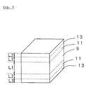
- a dielectric circuit board is made up of five sections.
- the material composition of section 9 between the dotted lines A and sections 13 on the outer sides of the dotted lines B are respectively uniform.
- sections 11 between the dotted lines A and B on the other hand, the material composition is different in different places. That is, as shown in Fig. 3, the dielectric constant of the board is constant in the sections 13, changes continuously in the sections 11 and is constant at a value higher than in the sections 13 in the central part 9 of the board.
- the form of the variation in the dielectric constant in sections 11 depends on the method by which materials of different compositions are combined in those sections of the board, and the variation can be either continuous (microscopically stepped) or stepped.
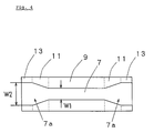
- the characteristic impedance of the strip line is the same in all parts of the strip line.
- the wide line width W2 provides connection spaces 7a for external wires to be attached, and in section 9 in the central part of the board, the narrow line width W1 makes possible high integration of strip lines.
- a ground electrode is formed on the rear side (not shown in the drawing) of the dielectric board.
- the dielectric board of Fig. 2 is made up of Mg-Si-Ti-O dielectric ceramics.
- Mg(OH) 2 , SiO 2 and TiO 2 as starting materials are mixed in the proportions shown in Table 2.
- the mixtures are then ground in a wet ball mill and powder form raw material mixtures numbered 1 to 9 are obtained.
- the raw material mixtures are pre-fired for 3 hours at 1150°C in air, and the pre-fired powders obtained are ground to an average particle diameter of about 1 ⁇ m using a wet ball mill.
- a binder polyvinyl butylene type
- a plasticizer dioctyl butylate type
- a dispersant sorbitan fatty acid ester type
- the central part 9 consists of green sheets comprising composition no. 9; sections 11 are formed by laminating green sheets comprising composition nos. 2 to 8 sequentially toward the central part 9, and outermost sections 13 consist of green sheets comprising composition no. 1.
- the compact is cut with a diamond cutter, in the direction in which it is laminated, into a sheet having a thickness of 3 mm.
- the laminate may be of sheet form, rectangular parallelopiped shaped or any other shape.
- the cut compact is heated at 500°C in air to remove the organic components. It is then further fired in air for two hours at 1370°C and a sintered body is thereby obtained.
- the obtained sintered body is polished to a thickness of 1.2 mm and a surface roughness of about 1 ⁇ m and further shaped with a diamond cutter to produce the dielectric board shown in Fig. 2.
- an Au ground electrode is formed over the whole rear surface of the dielectric board. Also, Au is deposited on the front surface of the dielectric board and by photolithography, a strip line of the pattern shown in Fig. 4 is formed so as to have a characteristic impedance of about 50 ⁇ .
- Mg-Ca-Ti-O dielectric ceramics of the compositions shown in Table 3 were made in the same way.
- Mg(OH) 2 , CaCO 3 and TiO 2 were used as the starting materials.
- These compositions, numbers 10 to 18, were disposed respectively in the same positions in a dielectric board as the compositions numbers 1 to 9 of the invention.
- comparison 1 The dielectric circuit board obtained using the compositions shown in Table 3 will hereinafter be referred to as comparison 1.
- Table 4 frequency characteristics, which show transmission loss, are shown in Table 4 for the dielectric circuit board of the preferred embodiment described above and for comparison 1.
- Table 4 frequency GHz 11.0 11.5 12.0 12.5 13.0 present invention db -0.3 -0.4 -0.5 -0.5 -0.6 comparison 1 db -3.6 -3.7 -3.9 -4.2 -4.5
Landscapes
- Engineering & Computer Science (AREA)
- Chemical & Material Sciences (AREA)
- Ceramic Engineering (AREA)
- Manufacturing & Machinery (AREA)
- Organic Chemistry (AREA)
- Structural Engineering (AREA)
- Materials Engineering (AREA)
- Inorganic Chemistry (AREA)
- Power Engineering (AREA)
- Compositions Of Oxide Ceramics (AREA)
- Microelectronics & Electronic Packaging (AREA)
- Inorganic Insulating Materials (AREA)
- Waveguides (AREA)
Applications Claiming Priority (2)
| Application Number | Priority Date | Filing Date | Title |
|---|---|---|---|
| JP34012/95 | 1995-02-22 | ||
| JP7034012A JPH08225371A (ja) | 1995-02-22 | 1995-02-22 | 誘電体磁器 |
Publications (1)
| Publication Number | Publication Date |
|---|---|
| EP0728716A1 true EP0728716A1 (de) | 1996-08-28 |
Family
ID=12402514
Family Applications (1)
| Application Number | Title | Priority Date | Filing Date |
|---|---|---|---|
| EP96102686A Withdrawn EP0728716A1 (de) | 1995-02-22 | 1996-02-22 | Dielektrische Keramik |
Country Status (2)
| Country | Link |
|---|---|
| EP (1) | EP0728716A1 (de) |
| JP (1) | JPH08225371A (de) |
Cited By (1)
| Publication number | Priority date | Publication date | Assignee | Title |
|---|---|---|---|---|
| EP1376749A1 (de) * | 2002-06-27 | 2004-01-02 | Harris Corporation | Breitband-Impedanzwandler |
Citations (2)
| Publication number | Priority date | Publication date | Assignee | Title |
|---|---|---|---|---|
| WO1984002521A1 (en) * | 1982-12-22 | 1984-07-05 | Tam Ceramics Inc | Low firing ceramic dielectric for temperature compensating capacitors |
| US4882650A (en) * | 1988-12-05 | 1989-11-21 | Sprague Electric Company | Magnesium titanate ceramic and dual dielectric substrate using same |
-
1995
- 1995-02-22 JP JP7034012A patent/JPH08225371A/ja active Pending
-
1996
- 1996-02-22 EP EP96102686A patent/EP0728716A1/de not_active Withdrawn
Patent Citations (2)
| Publication number | Priority date | Publication date | Assignee | Title |
|---|---|---|---|---|
| WO1984002521A1 (en) * | 1982-12-22 | 1984-07-05 | Tam Ceramics Inc | Low firing ceramic dielectric for temperature compensating capacitors |
| US4882650A (en) * | 1988-12-05 | 1989-11-21 | Sprague Electric Company | Magnesium titanate ceramic and dual dielectric substrate using same |
Cited By (2)
| Publication number | Priority date | Publication date | Assignee | Title |
|---|---|---|---|---|
| EP1376749A1 (de) * | 2002-06-27 | 2004-01-02 | Harris Corporation | Breitband-Impedanzwandler |
| US6737932B2 (en) | 2002-06-27 | 2004-05-18 | Harris Corporation | Broadband impedance transformers |
Also Published As
| Publication number | Publication date |
|---|---|
| JPH08225371A (ja) | 1996-09-03 |
Similar Documents
| Publication | Publication Date | Title |
|---|---|---|
| EP0506476B1 (de) | Dielektrische Filter mit Koppelelektroden um Resonatoren oder Elektroden zu Verbinden, und Verfahren zur Einstellung der Frequenzcharakteristik des Filters | |
| US7799718B2 (en) | Dielectric ceramic composition, complex electronic device and multilayer ceramic capacitor | |
| US20020009577A1 (en) | Electronic parts | |
| US11626232B2 (en) | Multilayer coil component | |
| US7161446B2 (en) | Noise filter | |
| JPH05183314A (ja) | 多層セラミック部品の製造方法および多層セラミック部品 | |
| EP0717018B1 (de) | Dielektrische, keramische Zusammensetzungen und dielektrische Resonatoren | |
| JPH08154006A (ja) | 誘電体基板 | |
| EP1575060B1 (de) | Dielektrische keramische Zusammensetzung und mehrschichtiges keramisches Bauteil enthaltend diese Zusammensetzung | |
| EP1160909B1 (de) | Zweimoden-Bandpassfilter | |
| US6356244B1 (en) | Antenna device | |
| US5948718A (en) | Dielectric ceramic polarizer | |
| JP3846464B2 (ja) | 誘電体セラミック組成物およびこれを用いたセラミック電子部品 | |
| US7205254B2 (en) | Dielectric ceramic composition and multilayer ceramic part | |
| EP1310468A2 (de) | Dielektrische Porzellanzusammensetzung | |
| JPH05152804A (ja) | 誘電体フイルター及びその周波数特性の調整方法 | |
| EP0558319B1 (de) | Dielektrische keramische Zusammensetzungen und diese verwendende Mikrowellengeräte | |
| JP3772912B2 (ja) | 誘電体磁器、誘電体基板および移相器 | |
| JPH07283619A (ja) | 誘電体基板 | |
| JP3889179B2 (ja) | アンテナ装置 | |
| JP2536820B2 (ja) | Lc複合部品 | |
| JP3373436B2 (ja) | セラミック積層電子部品 | |
| JP3754778B2 (ja) | 高周波用磁器組成物、高周波用磁器およびその製造方法 | |
| JP3193157B2 (ja) | 低温焼成用誘電体磁器組成物及びそれを用いて得られた誘電体共振器若しくは誘電体フィルター並びにそれらの製造方法 | |
| JPH08225371A (ja) | 誘電体磁器 |
Legal Events
| Date | Code | Title | Description |
|---|---|---|---|
| PUAI | Public reference made under article 153(3) epc to a published international application that has entered the european phase |
Free format text: ORIGINAL CODE: 0009012 |
|
| AK | Designated contracting states |
Kind code of ref document: A1 Designated state(s): DE FR GB |
|
| 17P | Request for examination filed |
Effective date: 19960911 |
|
| 17Q | First examination report despatched |
Effective date: 19970625 |
|
| STAA | Information on the status of an ep patent application or granted ep patent |
Free format text: STATUS: THE APPLICATION IS DEEMED TO BE WITHDRAWN |
|
| 18D | Application deemed to be withdrawn |
Effective date: 19971106 |