EP0729400B1 - Sicherheitsnullstelleinrichtung - Google Patents
Sicherheitsnullstelleinrichtung Download PDFInfo
- Publication number
- EP0729400B1 EP0729400B1 EP95901663A EP95901663A EP0729400B1 EP 0729400 B1 EP0729400 B1 EP 0729400B1 EP 95901663 A EP95901663 A EP 95901663A EP 95901663 A EP95901663 A EP 95901663A EP 0729400 B1 EP0729400 B1 EP 0729400B1
- Authority
- EP
- European Patent Office
- Prior art keywords
- reset
- output
- input
- channel
- closed
- Prior art date
- Legal status (The legal status is an assumption and is not a legal conclusion. Google has not performed a legal analysis and makes no representation as to the accuracy of the status listed.)
- Expired - Lifetime
Links
- 239000003990 capacitor Substances 0.000 claims description 24
- 238000010586 diagram Methods 0.000 description 4
- 230000002950 deficient Effects 0.000 description 1
- 238000004519 manufacturing process Methods 0.000 description 1
- 238000012986 modification Methods 0.000 description 1
- 230000004048 modification Effects 0.000 description 1
- 238000012544 monitoring process Methods 0.000 description 1
- 230000003068 static effect Effects 0.000 description 1
Images
Classifications
-
- F—MECHANICAL ENGINEERING; LIGHTING; HEATING; WEAPONS; BLASTING
- F16—ENGINEERING ELEMENTS AND UNITS; GENERAL MEASURES FOR PRODUCING AND MAINTAINING EFFECTIVE FUNCTIONING OF MACHINES OR INSTALLATIONS; THERMAL INSULATION IN GENERAL
- F16P—SAFETY DEVICES IN GENERAL; SAFETY DEVICES FOR PRESSES
- F16P3/00—Safety devices acting in conjunction with the control or operation of a machine; Control arrangements requiring the simultaneous use of two or more parts of the body
- F16P3/12—Safety devices acting in conjunction with the control or operation of a machine; Control arrangements requiring the simultaneous use of two or more parts of the body with means, e.g. feelers, which in case of the presence of a body part of a person in or near the danger zone influence the control or operation of the machine
- F16P3/14—Safety devices acting in conjunction with the control or operation of a machine; Control arrangements requiring the simultaneous use of two or more parts of the body with means, e.g. feelers, which in case of the presence of a body part of a person in or near the danger zone influence the control or operation of the machine the means being photocells or other devices sensitive without mechanical contact
- F16P3/144—Safety devices acting in conjunction with the control or operation of a machine; Control arrangements requiring the simultaneous use of two or more parts of the body with means, e.g. feelers, which in case of the presence of a body part of a person in or near the danger zone influence the control or operation of the machine the means being photocells or other devices sensitive without mechanical contact using light grids
-
- H—ELECTRICITY
- H01—ELECTRIC ELEMENTS
- H01H—ELECTRIC SWITCHES; RELAYS; SELECTORS; EMERGENCY PROTECTIVE DEVICES
- H01H47/00—Circuit arrangements not adapted to a particular application of the relay and designed to obtain desired operating characteristics or to provide energising current
- H01H47/002—Monitoring or fail-safe circuits
- H01H47/004—Monitoring or fail-safe circuits using plural redundant serial connected relay operated contacts in controlled circuit
- H01H47/005—Safety control circuits therefor, e.g. chain of relays mutually monitoring each other
Definitions
- the present invention relates to a safety reset device intended for use together with a personal safety protection device, comprising a reset switch; means for generating a reset signal, said generating means being so arranged that the reset switch must have been both closed and opened to generate the reset signal; two reset channels, each comprising an input from a personal safety protection device, an output, holding means for the output and starting means arranged to close the output and activate the holding means when a reset signal is received and the input is closed.
- Personal safety protection devices are used, for example, around industrial robots to prevent personnel from entering the working area of the robot and risking to be injured when the robot is still operating.
- a personal safety protection device may consist of light beams or light curtains forming a border around the working area of the robot and emitting a stop signal to the robot when broken, or a contact mat emitting a stop signal to the robot when stepped on, or a fence having a gate emitting a stop signal when opened, or the like.
- the personal safety protection devices are generally doubled, such that, if one fails, a stop should nevertheless be obtained by means of the other.
- the personal safety protection devices and the reset switch are coupled to a safety reset device monitoring the inputs from the personal safety protection devices in such a manner that both outputs to the robot can only be closed if both inputs from the personal safety protection devices are closed.
- a safety reset device monitoring the inputs from the personal safety protection devices in such a manner that both outputs to the robot can only be closed if both inputs from the personal safety protection devices are closed.
- the reset switch which must have been both closed and opened to make it possible to close the outputs.
- the reset button is short-circuited, no reset signal is generated.
- the outputs are also monitored, implying that both must have been opened before resetting in order to enable them to be closed when the reset signal is received.
- Swedish Patent SE-B-465 067 describes a safety reset device according to the preamble of claim 1 and having two reset channels with a respective input from the personal safety protection device and also a reset switch, which, when it is closed and the outputs are open, operates a first relay, entailing the charging of a capacitor.
- the reset switch When the reset switch is opened, the first relay is released and the capacitor is discharged through a second relay.
- the second relay has a relay contact in each reset channel.
- a third relay is operated, which is located in this reset channel.
- the third relay becomes holding and closes the pertaining output to a machine.
- the second reset channel operates in the same way.
- This known safety reset device thus contains four relays. As is known, relays are however expensive and bulky components. It therefore is desirable to provide a safety reset device which has an equally reliable function, but which is less expensive and less bulky.
- the starting means and the holding means are completely made up of electronic components, thus making it possible to reduce the number of relays.
- the starting means and the holding means may use an output relay for their function within the scope of the invention.
- the starting means and the holding means might consist of one and the same component.
- Exchanging relays for electronic components however means that the device becomes more sensitive to interference.
- This problem has been solved by the corresponding electronic components in the two channels being substantially electrically mirror-inverted. If one component in the first reset channel operates closing to plus, the corresponding component in the other channel thus operates closing to minus. Since interference generally is either positive or negative, this means that there is but a very small risk that the corresponding components in the two channels should be affected, which in turn means that there is a minimal risk that the two channels should at the same time incorrectly close the outputs or fail to open the outputs upon receipt of a stop signal from an input.
- the means for generating a reset signal are completely made up of electronic components, making it possible to further reduce the number of relays.
- the electronic components may, in each reset channel, consist of e.g. a microprocessor.
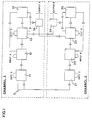
- Fig. 1 shows an embodiment of a safety reset device according to the invention, comprising two reset channels 1 , 2 and a reset switch 3 common to these channels.
- Each reset channel comprises in series a reset circuit 11 and 21, respectively, for generating a reset signal, which may be static or pulsed, an input circuit 12 and 22, respectively, having an input A and B, respectively, from a personal safety protection device, a starting circuit 13 and 23, respectively, connected to an output relay 14 and 24, respectively, and a holding circuit 15 and 25, respectively, in turn connected to the input 12 and 22, respectively.
- the starting circuits 13 and 23 also have an input from the output relay 24 and 14, respectively, in the other reset channel.
- the device operates as follows.
- the reset circuits 11 and 21 When the reset switch 3 has been closed and is thereafter opened, the reset circuits 11 and 21 generate a respective reset signal, which, if the inputs A and B in the input circuits 12 and 22, respectively, are closed, is passed on to the starting circuits 13 and 23, respectively, operating the output relays 14 and 24, respectively, if the output relays 24 and 14, respectively, in the other reset channel are released or have been closed a shorter time than a predetermined time.
- the starting circuit also activates the holding circuits 15 and 25, respectively, holding the output relay operated as long as the inputs A and B, respectively, are closed.
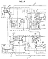
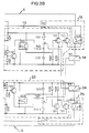
- Fig. 2 shows a circuit diagram for the embodiment of the invention shown in Fig. 1.
- the components corresponding to the respective blocks in Fig. 1 have been encircled and identified by reference numerals.
- the reset circuit 11 comprises a resistor R116 and a capacitor C102 which are connected in series between the supply voltage +24V and ground.
- a diode D101 is connected in parallel in the reverse direction over the resistor R116.
- the junction between the resistor R116 and the capacitor C102 is connected to the base of a pnp transistor T107, whose collector is connected to the supply voltage and whose emitter is connected to a resistor R117, connected in series with the light-emitting diode in an optocoupler O203 in the other channel 2.
- a resistor R100 in series with a capacitor C100 is connected between the supply voltage and ground.
- the junction between the resistor R100 and the capacitor C100 is connected to the cathode of the light-emitting diode in an optocoupler O100, and to the collector of the transistor in another optocoupler O104.
- the anode of the light-emitting diode in this optocoupler O104 is connected to the first pole of the reset switch 3, whose second pole is connected to the cathode of the light-emitting diode in the optocoupler O203.
- the cathode of the light-emitting diode in the optocoupler O104 is connected to ground, as is also the emitter of the transistor of the same optocoupler.
- the anode of the light-emitting diode in the optocoupler O100 is connected to the junction between the cathode of the light-emitting diode in the optocoupler O203 and the second pole of the reset switch 3, while its cathode is connected to a first pole of an automatic reset input A, whose second pole is connected to ground.
- the automatic reset input Auto A is strapped.
- the collector of the transistor in the optocoupler O100 is connected to a resistor R101, in turn connected to the supply voltage.
- the collector is further connected to the base of an npn transistor T100.
- the emitter of the transistor of the optocoupler O100 is connected to ground, like the emitter of the transistor T100.
- the collector of the transistor T100 is connected via a resistor R102 to the supply voltage and also forms an output which is connected to the starting circuit 13.
- the reset circuit 21 is designed in a corresponding way, but is electrically mirror-inverted. Components having equivalent parts in the reset circuit 11 are designated by the same reference numerals, the first figure, however, being 2 instead of 1. Moreover, it should be pointed out that the transistors T200 and T207 are pnp transistors.
- the reset circuit 11 operates as follows. When the reset switch 3 is closed, the current circuit from the transistor T107 closes to minus via the resistor R117, the light-emitting diode in the optocoupler O203, the light-emitting diode in the optocoupler O204, the reset switch 3 and the light-emitting diode in the optocoupler O104, the light-emitting diodes in the optocoupler O203 and the optocoupler O104 being lit.
- the voltage over the light-emitting diode in the optocoupler O100 which is equal to the voltage over the light-emitting diode in the optocoupler O104 minus the collector-emitter voltage over the transistor in the same optocoupler, is however too small in order that this should be lit.
- the capacitor C100 which before the closing of the reset switch 3, has been charged via the resistor R100, is discharged when closing the reset switch through the transistor in the optocoupler O104. When the reset switch 3 is thereafter opened, the capacitor C100 is again charged via the resistor R100 and the light-emitting diode in the optocoupler O100.
- the voltage over the light-emitting diode LO100 becomes sufficiently high for a short time for this to be lit. It is lit until the potential on the cathode of the light-emitting diode becomes too high on account of the charging of the capacitor C100.
- the light-emitting diode LO100 When the light-emitting diode LO100 is lit, its transistor becomes conducting, the previously conducting transistor T100 being cut off so as to generate a positive reset signal on the output of its collector. This reset signal is forwarded to the input circuit 12.
- the voltage on the cathode of the light-emitting diode in the optocoupler O100 must be higher than or equal to the voltage on its anode minus the ignition voltage of the light-emitting diode. Since the capacitor C100 may be discharged upon voltage turn-on, the voltage on the anode of the light-emitting diode must rise more slowly than the voltage over the capacitor. This is ensured by the capacitor C100, the resistor R116, the diode 101 and the transistor T107 if R116 * C102 exceeds R100 * C100.
- the reset circuit 21 operates in a corresponding manner and emits on its output a negative reset signal.
- the input circuit 12 comprises an input A from a personal safety protection device, this input being connected to ground.
- the positive pole of the input is connected to a resistor R115, in turn connected to the cathode of a light-emitting diode in an optocoupler O103.
- the anode of the light-emitting diode is connected to the collector of a pnp transistor T106, whose emitter is connected to the supply voltage via a strapped input.
- the emitter of the transistor in the optocoupler O103 is connected to ground, while its collector is connected to the cathode of a diode D100, whose anode is connected to the emitter of an npn transistor T101, the base of which is connected to the output of the reset circuit 11 and the collector of which forms the output to the starting circuit 13.
- the input circuit 22 lacks the optocoupler O103 and the resistor 115, but otherwise is made up of the same components as the input circuit 12. Moreover, it is electrically mirror-inverted in relation to the input circuit 12.
- the input circuit 12 operates in the following way.
- the input A When the input A is closed, the light-emitting diode in the optocoupler O103 is lit, the transistor in this optocoupler becoming conducting, such that the cathode of the diode D100 has a low voltage. If a reset signal is then obtained from the reset circuit 11 on the base of the transistor T101, this becomes conducting and generates a reset signal on the collector output to the starting circuit 13. If, on the other hand, the input A is not closed when the reset signal comes from the reset circuit 11, the transistor T101 does not become conducting and no reset signal is received on the output of the input circuit 12.
- the input circuit 22 operates as follows.
- the starting circuit 13 includes three resistors R103, R104 and R105 connected in series between the supply voltage and ground.
- the output from the input circuit 12 is connected to the junction between the resistors R103 and R104.
- the junction between the resistor R104 and the resistor R105 is connected to the base of an npn transistor T102, whose emitter is connected to ground and whose collector is connected to the anode of a light-emitting diode in an optocoupler O101, the cathode of the light-emitting diode being connected to ground.
- the collector of the transistor of the optocoupler O101 is connected to the supply voltage, while its emitter is connected to ground via a resistor R108.
- the anode of the light-emitting diode in the optocoupler O101 is further connected to the resistor R106, in turn connected to the junction between a capacitor C101, whose other pole is connected to ground, and two series-connected relay contacts, one of which consists of the test input B and the other of a relay contact for the output relay 24 in the other channel 2.
- the junction between the emitter of the transistor in the optocoupler O101 and the resistor R108 is connected to the base of a pnp transistor T103, whose emitter is connected to the supply voltage and whose collector is connected to ground via a resistor R109.
- the collector of the transistor T103 is also connected to the base of a pnp transistor T104, whose emitter is connected to the supply voltage and whose collector is connected to the output relay 14 and to the holding circuit 15.
- the starting circuit 23 is made up in a corresponding manner, but with electrical mirror-inversion, the transistor T202 being a pnp transistor and the transistors T203 and T204 being npn transistors.
- the purpose of the starting circuits is, when a reset signal is received on the output from the input circuit, to operate the output relay and activate the holding circuit which should then hold the relay operated until the input is closed.
- the starting circuits there is a simultaneity requirement between the two reset channels, which means that one starting circuit can only operate the output relay if the output relay in the other channel is released or has been operated maximally for a predetermined time.
- the simultaneity requirement functions as follows in respect of the first reset channel: When the output relay 24 in the second reset channel has been released, the capacitor C101 is charged via the test input Test B and the control contact for the output relay 24. When one of these contacts is opened, the capacitor C101 is disconnected from the supply voltage and instead starts being discharged through either the light-emitting diode in the optocoupler O101 or the transistor T102. When there is no reset signal, the transistor T102 is conducting and thus short-circuits the light-emitting diode in the optocoupler O101, the capacitor C101 being discharged through the capacitor T102, and nothing else happens.
- the transistor T102 If a reset signal is received on the output from the transistor T101, the transistor T102 is cut off and the capacitor is then discharged via the light-emitting diode in the optocoupler O101. The light-emitting diode is then lit and causes its associated transistor to become conducting, the transistor T103 being cut off and the transistor T104 becomes conducting with the aid of the resistor R109 and operates the output relay 14.
- the size of the capacitor C101 thus determines the interval within which the two output relays 14 and 24 must operate. When the capacitor C101 is discharged, the relay 14 cannot be operated any more.
- the starting circuit 23 acts in a corresponding manner.
- the holding circuit 15 comprises an optocoupler O102 whose light-emitting diode has its anode connected to the output relay 14 and its cathode connected to a resistor R107, in turn connected to the transistor in the optocoupler O103 in the input circuit 12.
- the resistor R107 serves to limit the current to the light-emitting diode in the optocoupler O102.
- the transistor of the optocoupler O102 has an emitter which is connected to the output relay 14 and a collector which is connected to the junction between the resistor R117 and the emitter of the transistor T107 in the input circuit.
- the reason why the collector of the transistor in the optocoupler O102 is connected to the transistor T107 and the resistor R117 and not directly to the supply voltage is that the voltage on the collector of the transistor should rise slowly upon voltage turn-on. If the voltage does not rise slowly and the input A is closed, there is a risk that a pulse of short duration, upon voltage turn-on, will pass through to the emitter of the transistor, in which case the light-emitting diode can be lit and open the transistor which operates the relay. When the starting circuit 13 operates the output relay 14 and the input A is closed, the light-emitting diode in the optocoupler O102 is lit, and its transistor becomes conducting.
- the holding circuit 25 is designed and operates in a corresponding manner.
- the reset device is so designed that it should be possible to connect the inputs A and B directly to a contact mat.
- the two outputs of a contact mat are always closed. When the mat is acted on, the outputs are short-circuited to each other. This should then result in that the two output relays 14, 24 are released. Since the input B closes to the supply voltage, while the input A closes to ground, a short-circuit between the inputs means that the supply voltage is short-circuited. Therefore, the reset device is provided with current limiting means 16 and 26 in the reset channels 1 and 2, respectively.
- the current limiting means 26 comprise an npn transistor T205, whose collector is connected to the supply voltage and whose emitter is connected to a resistor R210, in turn connected to the input B.
- the current limiting means 26 further comprise an npn transistor 206 whose base is connected to the junction between the emitter of the transistor 205 and the resistor 210, whose emitter is connected to the input B and whose collector is connected via a resistor 211 to the supply voltage.
- the current through the resistor R210 then increases until the voltage drop over the resistor becomes so high that the transistor T206 becomes conducting, the transistor 205 being cut off so as to limit the current. Since the input B is still at zero volt, the holding circuit is broken down and the output relay 24 is released.
- the current limiting means 16 in the reset channel 1 comprises three resistors R110, R111, R112, which are connected in series between the supply voltage and ground.
- the junction between the resistor R111 and R112 is connected via a diode D1 to the base of the transistor 205 in the other reset channel 2.
- the junction between the resistors R110 and R111 is connected to the base of an npn transistor T105, whose emitter is connected to ground and whose collector is connected via a resistor R113 to a pnp transistor T106, whose emitter is connected to the supply voltage and also to its base via a resistor R114 and whose collector is connected to the anode of the light-emitting diode in the optocoupler O103.
- the input A is supplied by the transistor T106, controlled by the transistor T105.
- the collector of the transistor T206 becomes close to zero volt, the transistor T105 being cut off, in turn cutting off the transistor T106.
- the lightemitting diode in the optocoupler O103 is turned off and, thus, the holding circuit 15 is broken down and the output relay 14 is released.
- the output relays 14, 24 can be replaced by transistor outputs, which can be adapted to drive external relays or contactors, whose contacts are monitored in the reset device.
- This solution has the advantage that the reset device becomes completely electronic and, hence, cheap to manufacture. If an external relay is defective, it can easily be exchanged.
- the reset circuits 11 and 12 may be made up differently and yet fulfil the same function.
- the capacitor might be designed so as to be charged/discharged via a transistor or optocoupler providing a reset signal when the reset switch is opened.
- the reset device may be provided with signal outputs in the form of transistors or optocouplers, which are connected in series with the optocouplers O102 and O202, respectively.
Landscapes
- Engineering & Computer Science (AREA)
- General Engineering & Computer Science (AREA)
- Mechanical Engineering (AREA)
- Electronic Switches (AREA)
- Debugging And Monitoring (AREA)
Claims (9)
- Sicherheits-Nullstelleinrichtung, bestimmt für den Gebrauch zusammen mit einer persönlichen Sicherheits-Schutzvorrichtung, enthaltend einen Rückstellschalter (3); Mittel (11, 21) zur Erzeugung eines Rückstellsignals, wobei die Erzeugungsmittel so vorgesehen sind, daß der Rückstellschalter (3) zwecks Erzeugung des Rückstellsignals sowohl geschlossen als auch geöffnet werden muß; zwei Rückstellkanäle (1, 2), die jeder eine Eingabe (A, B) von der persönlichen Sicherheits-Schutzvorrichtung, eine Ausgabe (14, 24), Haltemittel (15, 25) für die Ausgabe und Startmittel (13, 23) umfassen, die adaptiert sind zum Schließen der Ausgabe und Aktivieren der Haltemittel (15, 25), wenn ein Rückstellsignal empfangen und die Eingabe (A, B) geschlossen wird,
dadurch gekennzeichnet, daß
wenigstens die Startmittel (13, 23) und die Haltemittel (15, 25) volständig aus elektronischen Bauteilen bestehen, und daß entsprechende elektronische Bauteile in den Startmitteln und den Haltemitteln im wesentlichen elektronisch spiegelbildlich sind, so daß, wenn ein Bauteil an einen Pol der Stromversorgung in einem Rückstellkanal angeschlossen ist, das entsprechende Bauteil im anderen Rückstellkanal an den anderen Pol der Stromversorgung angeschlossen ist. - Einrichtung nach Anspruch 1, dadurch gekennzeichnet, daß die Mittel (11, 21) zur Erzeugung eines Rückstellsignals vollständig aus elektronischen Bauteilen bestehen, und daß jeder Rückstellkanal, getrennt von dem anderen Kanal, seine eigenen Mittel zur Erzeugung des Rückstellsignals hat.
- Einrichtung nach Anspruch 1 oder 2, dadurch gekennzeichnet, daß die elektronischen Bauteile einen Mikroprozessor in jedem Rückstellkanal (1, 2) umfassen.
- Einrichtung nach Anspruch 2, dadurch gekennzeichnet, daß die Mittel (11, 21) zur Erzeugung eines Rückstellsignals einen ersten Kondensator (C100; C200) umfassen, der entladen bzw. geladen wird, wenn der Rückstellschalter (3) geschlossen bzw. geöffnet wird, wobei der Ladungszustand des Kondensators die Spannung über einem ersten Schaltmittel (O100; O200) beeinflußt, das für kurze Zeit während des Ladevorgangs zur Erzeugung des Rückstellsignals betätigt wird.
- Einrichtung nach einem der vorhergehenden Ansprüche, dadurch gekennzeichnet, daß jeder der Rückstellkanäle (1, 2) außerdem ein zweites Schaltmittel (T101; T201) umfaßt, adaptiert zum Empfang des Rückstellsignals und derart mit der Eingabe (A, B) von der persönlichen Sicherheits-Schutzvorrichtung verbunden, daß es von dem Rückstellsignal geschlossen wird, wenn die Eingabe (A, B) geschlossen ist.
- Einrichtung nach einem der vorhergehenden Ansprüche, dadurch gekennzeichnet, daß jeder Rückstellkanal (1, 2) Strombegrenzer enthält, adaptiert zum Begrenzen des Stroms, wenn die Eingabe von der persönlichen Sicherheits-Schutzvorrichtung in dem einen Rückstellkanal mit der Eingabe von der persönlichen Sicherheits-Schutzvorrichtung in dem anderen Rückstellkanal kurzgeschlossen wird, wobei die Ausgaben (14, 24) geöffnet werden.
- Einrichtung nach einem der vorhergehenden Ansprüche, dadurch gekennzeichnet, daß die Startmittel (13, 23) jeweils einen Sensor zum Abfühlen des Zustandes der Ausgabe im anderen Kanal umfassen, wobei der Sensor adaptiert ist zum Verhüten des Schließens der Ausgabe seines Rückstellkanals, falls die Ausgabe in dem anderen Rückstellkanal länger als eine vorbestimmte Zeit geschlossen war, wenn das Rückstellsignal empfangen wird.
- Einrichtung nach Anspruch 7, dadurch gekennzeichnet, daß die Sensoren jeweils einen Kondensator (C101; C201) umfassen, der geladen wird, wenn die Ausgabe (24, 14) in dem anderen Rückstellkanal geöffnet wird, und der, wenn die Eingabe (A, B) von der persönlichen Sicherheits-Schutzvorrichtung in seinem Rückstellkanal geschlossen und das Rückstellsignal empfangen wird, über ein drittes Schaltmittel (O101; O201) entladen wird, das zum Schließen der Ausgabe adaptiert ist.
- Einrichtung nach Anspruch 8, dadurch gekennzeichnet, daß die Haltemittel (15, 25) aus einem Optokoppler (O102; O202) bestehen, dessen lichtemittierende Diode aktiviert wird, wenn das dritte Schaltmittel die Ausgabe schließt, und dessen Transistor die Ausgabe geschlossen hält, solange die Eingabe von der persönlichen Sicherheits-Schutzvorrichtung geschlossen ist.
Applications Claiming Priority (3)
| Application Number | Priority Date | Filing Date | Title |
|---|---|---|---|
| SE9303785A SE502306C2 (sv) | 1993-11-16 | 1993-11-16 | Säkerhetsåterställningsanordning |
| SE9303785 | 1993-11-16 | ||
| PCT/SE1994/001079 WO1995013906A1 (en) | 1993-11-16 | 1994-11-16 | Safety reset device |
Publications (2)
| Publication Number | Publication Date |
|---|---|
| EP0729400A1 EP0729400A1 (de) | 1996-09-04 |
| EP0729400B1 true EP0729400B1 (de) | 1998-08-05 |
Family
ID=20391768
Family Applications (1)
| Application Number | Title | Priority Date | Filing Date |
|---|---|---|---|
| EP95901663A Expired - Lifetime EP0729400B1 (de) | 1993-11-16 | 1994-11-16 | Sicherheitsnullstelleinrichtung |
Country Status (5)
| Country | Link |
|---|---|
| EP (1) | EP0729400B1 (de) |
| AU (1) | AU1081095A (de) |
| DE (1) | DE69412280T2 (de) |
| SE (1) | SE502306C2 (de) |
| WO (1) | WO1995013906A1 (de) |
Families Citing this family (4)
| Publication number | Priority date | Publication date | Assignee | Title |
|---|---|---|---|---|
| DE19626129C2 (de) * | 1996-06-28 | 2000-03-02 | Elan Schaltelemente Gmbh & Co | Sicherheitsschaltung |
| US20110308365A1 (en) * | 2008-04-24 | 2011-12-22 | Yuan Ze University | Safety device for machine tool |
| DE102009014248B4 (de) * | 2009-03-20 | 2012-06-14 | Sumitomo (Shi) Demag Plastics Machinery Gmbh | Begehbarer Sicherheitsboden |
| CN106313058B (zh) * | 2016-11-09 | 2018-11-20 | 兰州大学 | 一种输出多路高精度pwm信号的舵机控制装置 |
Family Cites Families (6)
| Publication number | Priority date | Publication date | Assignee | Title |
|---|---|---|---|---|
| JPS58213396A (ja) * | 1982-06-05 | 1983-12-12 | 竹中エンジニアリング工業株式会社 | 複眼式防犯センサ−システム |
| US4818866A (en) * | 1986-01-13 | 1989-04-04 | Data Instruments, Inc. | Intrusion detection system for operating industrial machines with variable sensitivity |
| EP0253000B1 (de) * | 1986-07-09 | 1990-01-24 | Tele-Security-Foto Überwachungsanlagen GmbH | Maschinenschutzschaltung |
| SE465067B (sv) * | 1988-03-24 | 1991-07-22 | Jokab Safety Ab | Anordning vid produktionsanpassade skyddssystem |
| WO1990008333A1 (en) * | 1988-11-04 | 1990-07-26 | Mats Linger | Safety guard beam light switch |
| SE463948B (sv) * | 1989-12-13 | 1991-02-11 | Gunnar Widell | Saett och anordning foer oevervakning av automatiska produktionsutrustnigar |
-
1993
- 1993-11-16 SE SE9303785A patent/SE502306C2/sv not_active IP Right Cessation
-
1994
- 1994-11-16 AU AU10810/95A patent/AU1081095A/en not_active Abandoned
- 1994-11-16 DE DE69412280T patent/DE69412280T2/de not_active Expired - Fee Related
- 1994-11-16 EP EP95901663A patent/EP0729400B1/de not_active Expired - Lifetime
- 1994-11-16 WO PCT/SE1994/001079 patent/WO1995013906A1/en not_active Ceased
Also Published As
| Publication number | Publication date |
|---|---|
| EP0729400A1 (de) | 1996-09-04 |
| SE9303785D0 (sv) | 1993-11-16 |
| SE502306C2 (sv) | 1995-10-02 |
| DE69412280T2 (de) | 1998-12-17 |
| SE9303785L (sv) | 1995-05-17 |
| DE69412280D1 (de) | 1998-09-10 |
| WO1995013906A1 (en) | 1995-05-26 |
| AU1081095A (en) | 1995-06-06 |
Similar Documents
| Publication | Publication Date | Title |
|---|---|---|
| US4523136A (en) | Safety arrangement for an adjustment installation of a seat adjustable manually or programmed | |
| JPH0347521B2 (de) | ||
| JPH0620348B2 (ja) | モータ制御回路の短絡を感知するための方法及び装置 | |
| US4025836A (en) | Protective system against commutation failure in a chopper circuit | |
| JPH0263067A (ja) | 画像作成装置の安全装置 | |
| EP0729400A1 (de) | Sicherheitsnullstelleinrichtung | |
| EP0011969B1 (de) | Sicherheitsschalter zur Abschaltung der Batterie eines Kraftfahrzeugs | |
| EP0944911B1 (de) | Sicherheitsrelais | |
| US3895346A (en) | Vehicle seat belt safety system | |
| US3588891A (en) | Self-monitoring field-contacts for automatic alarm systems | |
| US3940954A (en) | Electrical supervisory circuit arrangements | |
| JPS5818564B2 (ja) | 燃焼制御装置 | |
| US4262238A (en) | Controlled current supply circuit from a battery to a motor | |
| JPH03208735A (ja) | 車速自動制御装置 | |
| JPS5755428A (en) | Protection circuit | |
| JPH0473327B2 (de) | ||
| JP3662431B2 (ja) | 制御回路 | |
| JPS5835609A (ja) | 作業用機械 | |
| KR20010003625A (ko) | 자동식 소화기용 릴레이의 오동작 방지회로 | |
| JP3997676B2 (ja) | 非常停止回路 | |
| EP0078620A1 (de) | Schutzschaltung für Netzteil-Kontrolleinheit | |
| SU1298810A1 (ru) | Фотореле | |
| US3898475A (en) | Engine start prohibition system | |
| SU858048A2 (ru) | Устройство дл многоточечной сигнализации | |
| JPS60109677A (ja) | 電磁弁駆動装置 |
Legal Events
| Date | Code | Title | Description |
|---|---|---|---|
| PUAI | Public reference made under article 153(3) epc to a published international application that has entered the european phase |
Free format text: ORIGINAL CODE: 0009012 |
|
| 17P | Request for examination filed |
Effective date: 19960515 |
|
| AK | Designated contracting states |
Kind code of ref document: A1 Designated state(s): CH DE FR GB IT LI |
|
| GRAG | Despatch of communication of intention to grant |
Free format text: ORIGINAL CODE: EPIDOS AGRA |
|
| 17Q | First examination report despatched |
Effective date: 19970919 |
|
| GRAG | Despatch of communication of intention to grant |
Free format text: ORIGINAL CODE: EPIDOS AGRA |
|
| GRAH | Despatch of communication of intention to grant a patent |
Free format text: ORIGINAL CODE: EPIDOS IGRA |
|
| GRAH | Despatch of communication of intention to grant a patent |
Free format text: ORIGINAL CODE: EPIDOS IGRA |
|
| GRAA | (expected) grant |
Free format text: ORIGINAL CODE: 0009210 |
|
| AK | Designated contracting states |
Kind code of ref document: B1 Designated state(s): CH DE FR GB IT LI |
|
| PG25 | Lapsed in a contracting state [announced via postgrant information from national office to epo] |
Ref country code: LI Free format text: LAPSE BECAUSE OF FAILURE TO SUBMIT A TRANSLATION OF THE DESCRIPTION OR TO PAY THE FEE WITHIN THE PRESCRIBED TIME-LIMIT Effective date: 19980805 Ref country code: IT Free format text: LAPSE BECAUSE OF FAILURE TO SUBMIT A TRANSLATION OF THE DESCRIPTION OR TO PAY THE FEE WITHIN THE PRESCRIBED TIME-LIMIT;WARNING: LAPSES OF ITALIAN PATENTS WITH EFFECTIVE DATE BEFORE 2007 MAY HAVE OCCURRED AT ANY TIME BEFORE 2007. THE CORRECT EFFECTIVE DATE MAY BE DIFFERENT FROM THE ONE RECORDED. Effective date: 19980805 Ref country code: FR Free format text: LAPSE BECAUSE OF FAILURE TO SUBMIT A TRANSLATION OF THE DESCRIPTION OR TO PAY THE FEE WITHIN THE PRESCRIBED TIME-LIMIT Effective date: 19980805 Ref country code: CH Free format text: LAPSE BECAUSE OF FAILURE TO SUBMIT A TRANSLATION OF THE DESCRIPTION OR TO PAY THE FEE WITHIN THE PRESCRIBED TIME-LIMIT Effective date: 19980805 |
|
| REG | Reference to a national code |
Ref country code: CH Ref legal event code: EP |
|
| REF | Corresponds to: |
Ref document number: 69412280 Country of ref document: DE Date of ref document: 19980910 |
|
| EN | Fr: translation not filed | ||
| REG | Reference to a national code |
Ref country code: CH Ref legal event code: PL |
|
| PLBE | No opposition filed within time limit |
Free format text: ORIGINAL CODE: 0009261 |
|
| STAA | Information on the status of an ep patent application or granted ep patent |
Free format text: STATUS: NO OPPOSITION FILED WITHIN TIME LIMIT |
|
| 26N | No opposition filed | ||
| PGFP | Annual fee paid to national office [announced via postgrant information from national office to epo] |
Ref country code: GB Payment date: 20011107 Year of fee payment: 8 |
|
| PGFP | Annual fee paid to national office [announced via postgrant information from national office to epo] |
Ref country code: DE Payment date: 20011120 Year of fee payment: 8 |
|
| REG | Reference to a national code |
Ref country code: GB Ref legal event code: IF02 |
|
| PG25 | Lapsed in a contracting state [announced via postgrant information from national office to epo] |
Ref country code: GB Free format text: LAPSE BECAUSE OF NON-PAYMENT OF DUE FEES Effective date: 20021116 |
|
| PG25 | Lapsed in a contracting state [announced via postgrant information from national office to epo] |
Ref country code: DE Free format text: LAPSE BECAUSE OF NON-PAYMENT OF DUE FEES Effective date: 20030603 |
|
| GBPC | Gb: european patent ceased through non-payment of renewal fee |