EP0730283B1 - Thermistor et procédé de fabrication - Google Patents
Thermistor et procédé de fabrication Download PDFInfo
- Publication number
- EP0730283B1 EP0730283B1 EP96103174A EP96103174A EP0730283B1 EP 0730283 B1 EP0730283 B1 EP 0730283B1 EP 96103174 A EP96103174 A EP 96103174A EP 96103174 A EP96103174 A EP 96103174A EP 0730283 B1 EP0730283 B1 EP 0730283B1
- Authority
- EP
- European Patent Office
- Prior art keywords
- thermistor
- resistance
- devices
- thermistor devices
- trimming
- Prior art date
- Legal status (The legal status is an assumption and is not a legal conclusion. Google has not performed a legal analysis and makes no representation as to the accuracy of the status listed.)
- Expired - Lifetime
Links
Images


Classifications
-
- H—ELECTRICITY
- H01—ELECTRIC ELEMENTS
- H01C—RESISTORS
- H01C7/00—Non-adjustable resistors formed as one or more layers or coatings; Non-adjustable resistors made from powdered conducting material or powdered semi-conducting material with or without insulating material
-
- H—ELECTRICITY
- H01—ELECTRIC ELEMENTS
- H01C—RESISTORS
- H01C17/00—Apparatus or processes specially adapted for manufacturing resistors
- H01C17/22—Apparatus or processes specially adapted for manufacturing resistors adapted for trimming
- H01C17/24—Apparatus or processes specially adapted for manufacturing resistors adapted for trimming by removing or adding resistive material
- H01C17/242—Apparatus or processes specially adapted for manufacturing resistors adapted for trimming by removing or adding resistive material by laser
-
- H—ELECTRICITY
- H01—ELECTRIC ELEMENTS
- H01C—RESISTORS
- H01C1/00—Details
- H01C1/14—Terminals or tapping points specially adapted for resistors; Arrangements of terminals or tapping points on resistors
- H01C1/1406—Terminals or electrodes formed on resistive elements having positive temperature coefficient
-
- H—ELECTRICITY
- H01—ELECTRIC ELEMENTS
- H01C—RESISTORS
- H01C7/00—Non-adjustable resistors formed as one or more layers or coatings; Non-adjustable resistors made from powdered conducting material or powdered semi-conducting material with or without insulating material
- H01C7/02—Non-adjustable resistors formed as one or more layers or coatings; Non-adjustable resistors made from powdered conducting material or powdered semi-conducting material with or without insulating material having positive temperature coefficient
-
- Y—GENERAL TAGGING OF NEW TECHNOLOGICAL DEVELOPMENTS; GENERAL TAGGING OF CROSS-SECTIONAL TECHNOLOGIES SPANNING OVER SEVERAL SECTIONS OF THE IPC; TECHNICAL SUBJECTS COVERED BY FORMER USPC CROSS-REFERENCE ART COLLECTIONS [XRACs] AND DIGESTS
- Y10—TECHNICAL SUBJECTS COVERED BY FORMER USPC
- Y10T—TECHNICAL SUBJECTS COVERED BY FORMER US CLASSIFICATION
- Y10T29/00—Metal working
- Y10T29/49—Method of mechanical manufacture
- Y10T29/49002—Electrical device making
- Y10T29/49082—Resistor making
-
- Y—GENERAL TAGGING OF NEW TECHNOLOGICAL DEVELOPMENTS; GENERAL TAGGING OF CROSS-SECTIONAL TECHNOLOGIES SPANNING OVER SEVERAL SECTIONS OF THE IPC; TECHNICAL SUBJECTS COVERED BY FORMER USPC CROSS-REFERENCE ART COLLECTIONS [XRACs] AND DIGESTS
- Y10—TECHNICAL SUBJECTS COVERED BY FORMER USPC
- Y10T—TECHNICAL SUBJECTS COVERED BY FORMER US CLASSIFICATION
- Y10T29/00—Metal working
- Y10T29/49—Method of mechanical manufacture
- Y10T29/49002—Electrical device making
- Y10T29/49082—Resistor making
- Y10T29/49085—Thermally variable
Definitions
- the present invention relates to thermistor apparatuses and, more particularly, to an overcurrent-protection thermistor apparatus for protecting communications equipment such as telephone exchanges from overcurrent and to a manufacturing method thereof.
- an overcurrent-protection, positive-characteristics thermistor apparatus has been known.
- the known apparatus has one case in which two positive-characteristics thermistor devices are housed in order to protect communications equipment such as telephone exchanges from overcurrent, caused by lightning surges, contact with power lines or the like, intruding from communication lines. It is preferable that the difference in resistance between the two positive-characteristics thermistor devices is close to 0 ⁇ . This is because resistance matching needs to be maintained between the transmission and receiving circuit lines in communication circuits in communications equipment such as telephone exchanges.
- a method can be considered in which positive-characteristics thermistor devices are classified into groups according to their resistances and then thermistor devices in a certain group are paired. If the resistance of each of the two positive-characteristics thermistor devices is measured at different times, however, the measurement data may not be accurate due to a change in the ambient temperature at each measurement or a minute change due to aging of the resistance measuring instrument, thereby the difference in resistance between the two combined thermistor devices can become large. In the worst case, resistance matching between the transmission and receiving circuit lines cannot be maintained.
- Another method can be considered in which the resistance of each positive-characteristics thermistor device is measured and a device having a too-low resistance is trimmed to have a higher resistance such that all the thermistor devices have the specified resistance in the end. If the resistances of the two combined thermistor devices are measured at different times before they are trimmed, the measurement data may not be accurate due to the above-described reasons, making the difference in resistance measurements between the two thermistor devices inaccurate. Therefore, trimming cannot be conducted accurately and the resistance difference between the two thermistor devices can become large.
- a thermistor apparatus comprising: an insulating case; two thermistor devices housed in the insulating case; and two pairs of terminals to bracket the two thermistor devices respectively, wherein either one having a lower resistance of the two thermistor devices is trimmed to have a higher resistance which is substantially the same as the resistance of the other thermistor device.
- a manufacturing method of a thermistor apparatus comprising the steps of: providing an insulating case, two thermistor devices to be housed in the insulating case, and two pairs of terminals to bracket the two thermistor devices respectively; measuring the resistances of the two thermistor devices; and trimming whichever thermistor device has a lower resistance of the two thermistor devices to have a higher resistance which is substantially the same as the resistance of the other thermistor device.
- An advantageous embodiment comprises the steps of: providing an insulating case, two thermistor devices to be housed in the insulating case, and two pairs of terminals to bracket the two thermistor devices respectively; measuring the resistances of the two thermistor devices substantially at the same time; and trimming whichever has a lower resistance of the two thermistor devices to have a higher resistance which is substantially the same as the resistance of the other thermistor device.
- a further advantageous embodiment is described in Claim 4, through the provision of a manufacturing method of a thermistor apparatus according to Claim 3, wherein, in a condition in which the two thermistor devices are housed in the insulating case, the resistances of the two thermistor devices are measured at substantially the same time, and whichever has a lower resistance of the two thermistor devices is trimmed to have a higher resistance which is substantially the same as the resistance of the other device having a higher resistance between the two thermistor devices.
- a still further advantageous embodiment of the invention is described in Claim 5, through the provision of a manufacturing method of a thermistor apparatus according to Claim 3, wherein, in the condition in which the two thermistor devices are housed in the insulating case, the resistances of the two thermistor devices are measured at substantially the same time, and whichever has a lower resistance of the two thermistor devices is trimmed using a high-energy beam incident through an opening of the insulating case to have a higher resistance which is substantially the same as the resistance of the other thermistor device.
- trimming is only applied to one of the two thermistor devices and the other thermistor device needs not to be trimmed. Therefore, trimming work is halved compared with the conventional thermistor apparatus.
- the resistances of the two thermistor devices are measured nearly at the same time, hence such measurement is unlikely to be adversely influenced by effects caused by a change in the ambient temperature at the time of resistance measurement and a minute change by aging of the resistance measuring instrument. Therefore, the difference in resistance between the two thermistor devices is accurately measured and accurate trimming is applied to whichever thermistor device has a lower resistance.
- the easy-to-manufacture thermistor apparatus having a small difference in resistance between the two built-in thermistor devices can be consistently obtained.
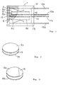
- a positive-thermistor apparatus comprises an insulating case 1, a lid member 2, two positive-characteristics thermistor devices 5 and 6, two planar terminals 10 and 11, two spring terminals 12 and 13, and an insulating plate 15.
- the insulating case 1 is closed at the left-hand opening with the lid member 2.
- Materials used for the insulating case 1 and the lid member 2 include thermosetting resin such as phenol and thermoplastic resin such as polyphenylene sulfide.
- the positive-characteristics thermistor devices 5 and 6 have circular shapes as shown in Figs. 2 and 3 and are made from ceramics such as BaTiO3.
- the thermistor devices 5 and 6 have electrodes 5a, 5b, 6a, and 6b at the respective front and rear surfaces. Whichever has a lower resistance of the two thermistor devices is trimmed to have a higher resistance such that its resistance is near the resistance of the other device, i.e., such that the two thermistor devices 5 and 6 have substantially the same resistance (for example, within a difference of ⁇ 1 ⁇ ).
- part of the electrode 6a of the thermistor device 6 is removed by laser trimming as shown in Fig. 3.
- the insulating plate 15 is interposed between the two thermistor devices 5 and 6 and it is made from a material having a good thermal conductivity and is formed integrally with the insulating case 1, for example.
- the planar terminals 10 and 11 are disposed between the insulating plate 15 and the thermistor device 5, and between the insulating plate 15 and the thermistor device 6, respectively.
- One planar terminal 10 touches a major surface of the insulating plate 15 and the electrode 5b of the thermistor device 5.
- the other planar terminal 11 touches the other wall surface of the insulating plate 15 and the electrode 6a of the thermistor device 6.
- One end 10a and 11a of both of the planar terminals 10 and 11 protrudes from the case 1 as shown at the right of Fig. 1.
- the spring terminals 12 and 13 are disposed between the case 1 and the thermistor device 5, and the case 1 and the thermistor device 6, respectively.
- the spring terminal 12 touches an inner surface of the case 1 and the electrode 5a of the thermistor device 5, and the spring terminal 13 touches inner surface of the case 1 and the electrode 6b of the thermistor device 6.
- One end 12a and 13a of both of the spring terminals 12 and 13 protrudes from the case 1 as shown at the right of Fig. 1.
- the two thermistor devices 5 and 6 are held by the terminals 12 and 13 with pressure applied in the devices' thickness direction.
- the thermistor devices 5 and 6 sandwich or bracket the planar terminals 10 and 11 and the insulating plate 15.
- the thermistor devices 5 and 6 are electrically insulated from each other by the insulating plate 15.
- the thermistor devices 5 and 6 are closely thermally-connected to each other through the insulating plate 15 and the planar terminals 10 and 11.
- two positive-characteristics thermistor devices 5 and 6 are selected and their resistances are measured with a resistance measuring instrument. It is preferred that the resistances of the two thermistor devices 5 and 6, which are to be housed in the same case, are measured at nearly the same time.
- the accurately measured resistance data is sent to a calculation processing unit.
- An electrode area to be removed from whichever thermistor device has a lower resistance between the two thermistor devices (e.g., in the first illustrated embodiment, the thermistor device 6) is calculated from the resistance difference between the two thermistor devices 5 and 6.
- a drive signal is sent from the calculation processing unit to a laser trimming unit.
- the laser trimming unit emits a laser beam to trim the thermistor device 6, which has a lower resistance in this example. In other words, a part of the electrode 6a is removed and the whole area of the electrode is reduced by the specified area.
- the thermistor device 6 in which part of the electrode 6a has been removed has a higher resistance than before, and is now substantially the same as that of the other thermistor device 5. Trimming can be conducted in two or more steps. The resistances of the thermistor devices may be measured subsequent to a first trimming, and trimming may be conducted again depending on the results of the first measurement.
- the two positive-characteristics thermistor devices 5 and 6 which have a small resistance difference are thus obtained. Since trimming is only applied to the thermistor device 6, which has a lower resistance, trimming work is halved compared with the conventional method in which trimming is applied to both thermistor devices.
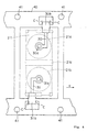
- a positive-characteristics thermistor apparatus comprises an insulating case 21, two positive-characteristics thermistor devices 25 and 26, two protruding terminals 30 and 31, and two spring terminals 32 and 33.
- the insulating case 21 has a partition 21c at its center and two circular cavities 21a and 21b disposed to the left and to the right of the partition within a plane.
- the thermistor devices 25 and 26 have circular shapes and are provided with electrodes 25a, 25b, 26a, and 26b at the respective front and rear surfaces. Whichever has a lower resistance of the two thermistor devices is trimmed to have a higher resistance. The higher resistance of the trimmed thermistor is near the resistance of the other device such that the two thermistor devices 25 and 26 have substantially the same resistance (for example, within a difference of ⁇ 1 ⁇ ).
- the protruding terminals 30 and 31 are insert-molded in the case 21 and are provided with protrusions 30a and 31a at their centers.
- the protrusions 30a and 31a project through holes 21d and 21e provided at the bottom of the case 21, and touch electrodes 25b and 26b of the thermistor devices 25 and 26, respectively.
- the other ends of the protruding terminals 30 and 31 are extended along the left and right side faces of the case 21 and folded on the surface of the case 21 to form external-connection portions 30b and 31b.
- the spring terminals 32 and 33 comprise electrodes 32a and 33a and external-connection portions 32b and 33b.
- the electrodes 32a and 33a are disposed on the upper surface of the case 21 and cover the openings of the cavities 21a and 21b.
- the external-connection portions 32b and 33b are folded along the surface of the case 21 to extend to the bottom surface by way of the left and right side faces of the case 21.
- another lid may be used to cover the openings.
- the two thermistor devices 25 and 26 are sandwiched or bracketed by the protruding terminals 30, 31 and the spring terminals 32, 33 in the cavities 21a and 21b, respectively, and held with pressure in the direction of the thickness of the thermistor devices.
- a hoop material 40 on which the protruding terminals 30 and 31 are connected is prepared by punching a strip-shaped metal plate as shown in Fig. 6.
- the hoop material 40 is provided with feed holes 41 at both edges and transferred using these holes in the direction indicated by arrow "a" to each process. Therefore, assembling and trimming can be conducted in one line as will be described later, thereby facilitating automation of the manufacturing process.
- the protruding terminals 30 and 31 are insert-molded with resin.
- the case 21 is formed, with the protrusions 30a and 31a and the external-connection portions 30b and 31b being exposed.
- the thermistor devices 25 and 26 are inserted horizontally into the cavities 21a and 21b of the case 21, as shown in Fig. 7.
- One measuring terminal 45a of a resistance measuring instrument 45 is inserted into a first hole 21d of the case 21 to touch a first protruding terminal 30.
- the other measuring terminal 45b is also inserted into a first cavity 21a to touch the first spring electrode 25a.
- one measuring terminal 46a of a second resistance measuring instrument 46 touches a second protruding terminal 31 and the other measuring terminal 46b touches a second electrode 26a.
- the resistances of the thermistor devices 25 and 26 are measured at the same time to avoid adverse effects caused by a change in the ambient temperature at resistance measurement and a minute change by aging of the resistance measuring instruments 45 and 46. Therefore the difference in resistance between the two thermistor devices 25 and 26 is accurately measured to conduct accurate trimming in a subsequent process.
- the measured, accurate resistance data is sent to a calculation processing unit 47 and an electrode area to be removed from whichever has a lower resistance between the two thermistor devices 25 and 26 (in the second embodiment, the left thermistor device 25 as shown in Fig. 4) is calculated from the resistance difference between the two thermistor devices. Then, according to the electrode area to be removed, a drive signal is sent from the calculation processing unit 47 to a laser trimming unit 50.
- the laser trimming unit 50 emits a laser beam L to trim the thermistor device 25, which has a lower resistance. In other words, a part of the electrode 25a, which is exposed through the opening portion of the cavity 21a, is removed and the whole area of the electrode is reduced by the specified area.
- the thermistor device 25 in which part of the electrode 25a has been removed has a higher resistance than before, the higher resistance being substantially the same as that of the other thermistor device 26.
- the two positive-characteristics thermistor devices 25 and 26 which have a small resistance difference are thus obtained. Since trimming is only applied to the thermistor device 25, which has a lower resistance, trimming work is halved compared with that for the conventional method in which trimming is applied to both thermistor devices. Since trimming as well as measuring resistance is conducted in the condition in which the thermistor devices 25 and 26 are housed in the case 21, smooth assembling can be performed and changes in resistance of the thermistor devices 25 and 26 due to cracks or chips occurring when the devices are handled can be prevented. Furthermore, foreign matter is unlikely to enter the case 21 since laser trimming is used.
- the spring terminals 32 and 33 are disposed at the openings of the cavities 21a and 21b in the case 21. Their external-connection portions 32b and 33b are folded along the surface of the case 21. Then, the positive-characteristics thermistor apparatus is taken out of the hoop material 40 by cutting the hoop material along a dot-and-dash line C shown in Fig. 6. The external-connection portions 30b and 31b of the protruded terminals 30 and 31 are folded along the surface of the case 21 to finish assembling the apparatus.
- a thermistor apparatus and a manufacturing method thereof according to the present invention is not limited to the foregoing embodiments. Within the scope of the invention, they can be modified in various manners.
- the thermistor apparatus using the positive-characteristics thermistor devices is described in the foregoing embodiments.
- the thermistor apparatus may use negative-characteristics thermistor devices.
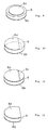
- An area removed from an electrode of the thermistor in trimming can have any shape. As shown in Fig. 9, for example, a circumferential area of the electrode 6a may be removed. Part of the upper electrode 6a and part of the lower electrode 6b may be removed as shown in Fig. 10. Alternatively, the electrode 6a may be divided into two sections as shown in Fig. 11. Part of the thermistor body can be removed together with the upper and lower electrodes 6a and 6b.
- a laser beam is used in trimming in the foregoing embodiments.
- a high-energy beam such as an electronic beam or an ion beam, can be used instead of the laser beam.
- the electrodes have a single layer in the foregoing embodiments. However, the electrodes may have multiple layers.
Landscapes
- Engineering & Computer Science (AREA)
- Microelectronics & Electronic Packaging (AREA)
- Physics & Mathematics (AREA)
- Electromagnetism (AREA)
- Ceramic Engineering (AREA)
- Optics & Photonics (AREA)
- Plasma & Fusion (AREA)
- Manufacturing & Machinery (AREA)
- Thermistors And Varistors (AREA)
- Apparatuses And Processes For Manufacturing Resistors (AREA)
Claims (5)
- Thermistor comprenant :dans lequel celui desdits deux éléments de thermistor (5, 6 ; 25, 26) présentant une résistance plus faible est ajusté pour présenter une résistance plus élevée qui est sensiblement identique à la résistance de l'autre élément de thermistor.un boítier isolant (1 ; 21) ;deux éléments de thermistor (5, 6 ; 25, 26) logés dans ledit boítier isolant ; etdeux paires de bornes (10, 11, 12, 13 ; 30, 31, 32, 33) pour entourer lesdits deux éléments de thermistor (5, 6 ; 25, 26) respectivement,
- Procédé de fabrication d'un thermistor comprenant les étapes consistant à :prévoir un boítier isolant (1 ; 21), deux éléments de thermistor (5, 6 ; 25, 26) à loger dans ledit boítier isolant (1 ; 21), et deux paires de bornes (10, 11, 12, 13 ; 30, 31, 32, 33) pour entourer lesdits deux éléments de thermistor (5, 6 ; 26, 26) respectivement ;mesurer les résistances desdits deux éléments de thermistor (5, 6 ; 25, 26) ; etajuster l'élément de thermistor qui possède une résistance plus faible desdits deux éléments de thermistor pour avoir une résistance plus élevée qui est identique à la résistance de l'autre élément.
- Procédé de fabrication selon la revendication 2, dans lequel les résistances desdits deux éléments de thermistor (5, 6 ; 25, 26) sont mesurées sensiblement simultanément.
- Procédé de fabrication selon la revendication 3, dans lequel lesdits deux éléments de thermistor (5, 6 ; 25, 26) sont logés dans ledit boítier isolant (1 ; 21) durant la mesure et l'ajustage.
- Procédé de fabrication selon la revendication 3, dans lequel ladite étape d'ajustage implique un faisceau à haute énergie frappant à travers une ouverture dudit boítier isolant (1 ; 21).
Applications Claiming Priority (3)
| Application Number | Priority Date | Filing Date | Title |
|---|---|---|---|
| JP43697/95 | 1995-03-03 | ||
| JP4369795 | 1995-03-03 | ||
| JP7043697A JPH08241802A (ja) | 1995-03-03 | 1995-03-03 | サーミスタ装置及びその製造方法 |
Publications (3)
| Publication Number | Publication Date |
|---|---|
| EP0730283A2 EP0730283A2 (fr) | 1996-09-04 |
| EP0730283A3 EP0730283A3 (fr) | 1997-06-18 |
| EP0730283B1 true EP0730283B1 (fr) | 2001-12-12 |
Family
ID=12671029
Family Applications (1)
| Application Number | Title | Priority Date | Filing Date |
|---|---|---|---|
| EP96103174A Expired - Lifetime EP0730283B1 (fr) | 1995-03-03 | 1996-03-01 | Thermistor et procédé de fabrication |
Country Status (6)
| Country | Link |
|---|---|
| US (2) | US5798685A (fr) |
| EP (1) | EP0730283B1 (fr) |
| JP (1) | JPH08241802A (fr) |
| KR (1) | KR100200950B1 (fr) |
| CN (1) | CN1084519C (fr) |
| DE (1) | DE69617772T2 (fr) |
Cited By (1)
| Publication number | Priority date | Publication date | Assignee | Title |
|---|---|---|---|---|
| EP4187172A1 (fr) * | 2021-11-25 | 2023-05-31 | BorgWarner Inc. | Procédé de confection de résistances, résistance et dispositif de chauffage |
Families Citing this family (22)
| Publication number | Priority date | Publication date | Assignee | Title |
|---|---|---|---|---|
| AU9282598A (en) * | 1997-10-03 | 1999-04-27 | K.K. Raychem | Electric assembly and device |
| US5953811A (en) * | 1998-01-20 | 1999-09-21 | Emc Technology Llc | Trimming temperature variable resistor |
| FR2795520B1 (fr) * | 1999-06-24 | 2001-09-07 | Remy Kirchdoerffer | Procede de fabrication d'un dispositif du type instrument ou appareil de mesure ou de detection et dispositifs resultants |
| US6304166B1 (en) * | 1999-09-22 | 2001-10-16 | Harris Ireland Development Company, Ltd. | Low profile mount for metal oxide varistor package and method |
| US6208233B1 (en) * | 2000-03-03 | 2001-03-27 | Delphi Technologies, Inc. | Trim resistor connector and sensor system |
| JP2002048655A (ja) * | 2000-05-24 | 2002-02-15 | Ngk Spark Plug Co Ltd | 温度センサ及びその製造管理方法 |
| JP4780689B2 (ja) * | 2001-03-09 | 2011-09-28 | ローム株式会社 | チップ抵抗器 |
| US20040095225A1 (en) * | 2001-03-19 | 2004-05-20 | Nelson Charles Scott | Independently housed trim resistor and a method for fabricating same |
| US20060091994A1 (en) * | 2001-03-19 | 2006-05-04 | Nelson Charles S | Independently housed trim resistor and a method for fabricating same |
| US6469254B1 (en) | 2001-08-08 | 2002-10-22 | Delphi Technologies, Inc. | Thermistor assembly holding device |
| DE10243113A1 (de) * | 2002-09-17 | 2004-04-01 | Epcos Ag | Elektrische Baugruppe und deren Verwendung |
| US6875631B2 (en) * | 2002-09-27 | 2005-04-05 | Renesas Technology Corp. | Semiconductor device and a method of manufacturing the same |
| US7161461B1 (en) | 2006-03-07 | 2007-01-09 | Delphi Technologies, Inc. | Injection molded trim resistor assembly |
| DE102006053081A1 (de) * | 2006-11-10 | 2008-05-15 | Epcos Ag | Elektrische Baugruppe mit PTC-Widerstandselementen |
| DE102006053085A1 (de) * | 2006-11-10 | 2008-05-15 | Epcos Ag | Elektrische Baugruppe mit PTC-Widerstandselementen |
| DE102007042358B3 (de) * | 2007-09-06 | 2008-11-20 | Epcos Ag | Elektrische Schutzvorrichtung |
| WO2009038418A2 (fr) * | 2007-09-21 | 2009-03-26 | Samhyun Cns Co., Ltd | Varistance et appareil à varistance |
| FR2958788B1 (fr) * | 2010-04-09 | 2015-01-30 | Abb France | Varistance comprenant une electrode avec une partie en saillie formant pole et parafoudre comprenant une telle varistance |
| FR2958787B1 (fr) * | 2010-04-09 | 2012-05-11 | Abb France | Dispositif de protection contre les surtensions a deconnecteurs thermiques dedoubles |
| CN102723155B (zh) * | 2012-07-09 | 2016-12-07 | 深圳市辰驹电子科技有限公司 | 可调值过流过压保护器 |
| JP5761211B2 (ja) * | 2013-01-11 | 2015-08-12 | 株式会社デンソー | ペア温度センサ及びその製造方法 |
| CN106782955B (zh) * | 2017-01-10 | 2018-08-17 | 广东百圳君耀电子有限公司 | 带过热保护的压敏电阻元件 |
Family Cites Families (29)
| Publication number | Priority date | Publication date | Assignee | Title |
|---|---|---|---|---|
| US2010814A (en) * | 1932-03-07 | 1935-08-13 | Ohio Electric Mfg Company | Protective device |
| US2382024A (en) * | 1943-04-24 | 1945-08-14 | Bell Telephone Labor Inc | Resistor and method of making it |
| US2609644A (en) * | 1949-09-10 | 1952-09-09 | Garrett Corp | Method of processing electrical elements |
| US3768157A (en) * | 1971-03-31 | 1973-10-30 | Trw Inc | Process of manufacture of semiconductor product |
| US3914727A (en) * | 1974-01-02 | 1975-10-21 | Sprague Electric Co | Positive-temperature-coefficient-resistor package |
| LU71901A1 (fr) * | 1974-07-09 | 1975-08-20 | ||
| NL165020C (nl) * | 1974-12-16 | 1981-02-16 | Philips Nv | Kleurentelevisie-ontvanger bevattende een ontmagneti- seerschakeling en samengesteld thermistorelement voor toepassing in een dergelijke schakeling. |
| IT1074590B (it) * | 1976-07-02 | 1985-04-20 | Necchi Spa | Scatola del rele di avviamento per motocompressori |
| NL7701813A (nl) * | 1977-02-21 | 1978-08-23 | Philips Nv | Verwarmingselement met een ptc-weerstands- lichaam. |
| US4200970A (en) * | 1977-04-14 | 1980-05-06 | Milton Schonberger | Method of adjusting resistance of a thermistor |
| US4419564A (en) * | 1981-03-30 | 1983-12-06 | Texas Instruments Incorporated | Self-regulating electric heater for use in an early fuel evaporation system |
| JPS57166474U (fr) * | 1981-04-13 | 1982-10-20 | ||
| FR2515445A1 (fr) * | 1981-10-28 | 1983-04-29 | Trt Telecom Radio Electr | Procede de realisation d'un pont d'alimentation soumis a des surcharges importantes et pont d'alimentation realise suivant ce procede |
| US4434416A (en) * | 1983-06-22 | 1984-02-28 | Milton Schonberger | Thermistors, and a method of their fabrication |
| US4792779A (en) * | 1986-09-19 | 1988-12-20 | Hughes Aircraft Company | Trimming passive components buried in multilayer structures |
| US4730103A (en) * | 1986-11-28 | 1988-03-08 | Gte Products Corporation | Compact PTC resistance heater |
| US5057964A (en) * | 1986-12-17 | 1991-10-15 | Northern Telecom Limited | Surge protector for telecommunications terminals |
| EP0327860A1 (fr) * | 1988-02-10 | 1989-08-16 | Siemens Aktiengesellschaft | Composant électrique du type pastille et son procédé de fabrication |
| SE460810B (sv) * | 1988-06-08 | 1989-11-20 | Astra Meditec Ab | Termistor avsedd foer temperaturmaetning samt foerfarande foer tillverkning av densamma |
| JPH03174701A (ja) * | 1989-09-22 | 1991-07-29 | Komatsu Ltd | サーミスタの製造方法および製造システム |
| JP2529252Y2 (ja) * | 1990-04-05 | 1997-03-19 | 日本油脂株式会社 | 正特性サーミスタ装置 |
| JPH0631685Y2 (ja) * | 1990-11-26 | 1994-08-22 | 太平洋精工株式会社 | ブロアモータ用抵抗器 |
| JPH0582305A (ja) * | 1991-04-05 | 1993-04-02 | Komatsu Ltd | 正特性サーミスタ |
| JPH0555006A (ja) * | 1991-08-29 | 1993-03-05 | Ngk Spark Plug Co Ltd | サーミスタ及びその製造方法 |
| JPH0543503U (ja) * | 1991-11-08 | 1993-06-11 | 日本油脂株式会社 | 正特性サーミスタ装置 |
| JPH0677007A (ja) * | 1992-08-26 | 1994-03-18 | Rohm Co Ltd | 円板型サーミスタの製造方法 |
| CN2144852Y (zh) * | 1992-10-29 | 1993-10-27 | 蔡雅凤 | 过电流保护快速响应正温度系数热敏电阻器 |
| JPH07106729A (ja) * | 1993-09-30 | 1995-04-21 | Murata Mfg Co Ltd | 厚膜回路部品の製造方法 |
| TW421413U (en) * | 1994-07-18 | 2001-02-01 | Murata Manufacturing Co | Electronic apparatus and surface mounting devices therefor |
-
1995
- 1995-03-03 JP JP7043697A patent/JPH08241802A/ja active Pending
-
1996
- 1996-02-29 US US08/608,722 patent/US5798685A/en not_active Expired - Lifetime
- 1996-03-01 EP EP96103174A patent/EP0730283B1/fr not_active Expired - Lifetime
- 1996-03-01 DE DE69617772T patent/DE69617772T2/de not_active Expired - Lifetime
- 1996-03-03 CN CN96106036A patent/CN1084519C/zh not_active Expired - Lifetime
- 1996-03-04 KR KR1019960005595A patent/KR100200950B1/ko not_active Expired - Lifetime
-
1998
- 1998-04-21 US US09/063,303 patent/US6188307B1/en not_active Expired - Lifetime
Cited By (2)
| Publication number | Priority date | Publication date | Assignee | Title |
|---|---|---|---|---|
| EP4187172A1 (fr) * | 2021-11-25 | 2023-05-31 | BorgWarner Inc. | Procédé de confection de résistances, résistance et dispositif de chauffage |
| US12417866B2 (en) | 2021-11-25 | 2025-09-16 | Borgwarner Inc. | Method for confectioning resistors, resistor, and heating device |
Also Published As
| Publication number | Publication date |
|---|---|
| CN1140887A (zh) | 1997-01-22 |
| EP0730283A3 (fr) | 1997-06-18 |
| CN1084519C (zh) | 2002-05-08 |
| KR100200950B1 (ko) | 1999-06-15 |
| DE69617772T2 (de) | 2002-05-23 |
| DE69617772D1 (de) | 2002-01-24 |
| JPH08241802A (ja) | 1996-09-17 |
| EP0730283A2 (fr) | 1996-09-04 |
| KR960035670A (ko) | 1996-10-24 |
| US6188307B1 (en) | 2001-02-13 |
| US5798685A (en) | 1998-08-25 |
Similar Documents
| Publication | Publication Date | Title |
|---|---|---|
| EP0730283B1 (fr) | Thermistor et procédé de fabrication | |
| US4747456A (en) | Load cell and temperature correction of the same | |
| US6269539B1 (en) | Fabrication method of connector having internal switch | |
| US4139726A (en) | Packaged microcircuit and method for assembly thereof | |
| KR100273173B1 (ko) | 임피던스를 제어하기 위한 상호 접속장치 및 방법 | |
| JP5942898B2 (ja) | 電子部品及び電子制御装置 | |
| KR100586128B1 (ko) | 회로기판으로의 온도퓨즈의 실장구조 | |
| CA1187953A (fr) | Barre omnibus a grande capacite comprenant des condensateurs ceramiques multicouches | |
| US7825677B2 (en) | Test jig for testing a packaged high frequency semiconductor device | |
| US5274352A (en) | Thick film resistive element, thick film printed circuit board and thick film hybrid integrated circuit device and their production methods | |
| US6128199A (en) | Composite device and manufacturing method thereof | |
| JPH0212002B2 (fr) | ||
| US7674038B2 (en) | Arrangement for temperature monitoring and regulation | |
| EP0635897B1 (fr) | Filtre diélectrique | |
| US6542066B1 (en) | Electric assembly and device | |
| US7333346B2 (en) | Circuit board having test coupon and method for evaluating the circuit board | |
| JP2004087851A (ja) | 回路基板およびパック電池 | |
| JP3022679B2 (ja) | 測定治具の校正部品 | |
| JPH09289402A (ja) | 非可逆回路素子 | |
| JP3002276B2 (ja) | 湿度センサ | |
| US4159507A (en) | Stripline circuit requiring high dielectrical constant/high G-force resistance | |
| JP2754916B2 (ja) | 標準コンデンサ | |
| US7105911B2 (en) | Multilayer electronic substrate, and the method of manufacturing multilayer electronic substrate | |
| JP3105444B2 (ja) | 電子部品評価用治具及び電子部品評価方法 | |
| JPH0338757B2 (fr) |
Legal Events
| Date | Code | Title | Description |
|---|---|---|---|
| PUAI | Public reference made under article 153(3) epc to a published international application that has entered the european phase |
Free format text: ORIGINAL CODE: 0009012 |
|
| 17P | Request for examination filed |
Effective date: 19960301 |
|
| AK | Designated contracting states |
Kind code of ref document: A2 Designated state(s): DE FR GB |
|
| PUAL | Search report despatched |
Free format text: ORIGINAL CODE: 0009013 |
|
| AK | Designated contracting states |
Kind code of ref document: A3 Designated state(s): DE FR GB |
|
| GRAG | Despatch of communication of intention to grant |
Free format text: ORIGINAL CODE: EPIDOS AGRA |
|
| 17Q | First examination report despatched |
Effective date: 20001120 |
|
| GRAG | Despatch of communication of intention to grant |
Free format text: ORIGINAL CODE: EPIDOS AGRA |
|
| GRAG | Despatch of communication of intention to grant |
Free format text: ORIGINAL CODE: EPIDOS AGRA |
|
| GRAH | Despatch of communication of intention to grant a patent |
Free format text: ORIGINAL CODE: EPIDOS IGRA |
|
| GRAH | Despatch of communication of intention to grant a patent |
Free format text: ORIGINAL CODE: EPIDOS IGRA |
|
| GRAA | (expected) grant |
Free format text: ORIGINAL CODE: 0009210 |
|
| AK | Designated contracting states |
Kind code of ref document: B1 Designated state(s): DE FR GB |
|
| REG | Reference to a national code |
Ref country code: GB Ref legal event code: IF02 |
|
| REF | Corresponds to: |
Ref document number: 69617772 Country of ref document: DE Date of ref document: 20020124 |
|
| ET | Fr: translation filed | ||
| PLBE | No opposition filed within time limit |
Free format text: ORIGINAL CODE: 0009261 |
|
| STAA | Information on the status of an ep patent application or granted ep patent |
Free format text: STATUS: NO OPPOSITION FILED WITHIN TIME LIMIT |
|
| 26N | No opposition filed | ||
| REG | Reference to a national code |
Ref country code: FR Ref legal event code: PLFP Year of fee payment: 20 |
|
| PGFP | Annual fee paid to national office [announced via postgrant information from national office to epo] |
Ref country code: DE Payment date: 20150224 Year of fee payment: 20 |
|
| PGFP | Annual fee paid to national office [announced via postgrant information from national office to epo] |
Ref country code: GB Payment date: 20150225 Year of fee payment: 20 Ref country code: FR Payment date: 20150309 Year of fee payment: 20 |
|
| REG | Reference to a national code |
Ref country code: DE Ref legal event code: R071 Ref document number: 69617772 Country of ref document: DE |
|
| REG | Reference to a national code |
Ref country code: GB Ref legal event code: PE20 Expiry date: 20160229 |
|
| PG25 | Lapsed in a contracting state [announced via postgrant information from national office to epo] |
Ref country code: GB Free format text: LAPSE BECAUSE OF EXPIRATION OF PROTECTION Effective date: 20160229 |