EP0731491A2 - Verfahren zur Herstellung einer Silizium-Schicht mit einer Oberfläche von kontrollierter Ebenheit bzw. Unebenheit - Google Patents
Verfahren zur Herstellung einer Silizium-Schicht mit einer Oberfläche von kontrollierter Ebenheit bzw. Unebenheit Download PDFInfo
- Publication number
- EP0731491A2 EP0731491A2 EP96103418A EP96103418A EP0731491A2 EP 0731491 A2 EP0731491 A2 EP 0731491A2 EP 96103418 A EP96103418 A EP 96103418A EP 96103418 A EP96103418 A EP 96103418A EP 0731491 A2 EP0731491 A2 EP 0731491A2
- Authority
- EP
- European Patent Office
- Prior art keywords
- silicon
- amorphous silicon
- film
- grains
- atoms
- Prior art date
- Legal status (The legal status is an assumption and is not a legal conclusion. Google has not performed a legal analysis and makes no representation as to the accuracy of the status listed.)
- Withdrawn
Links
- XUIMIQQOPSSXEZ-UHFFFAOYSA-N Silicon Chemical compound [Si] XUIMIQQOPSSXEZ-UHFFFAOYSA-N 0.000 title claims abstract description 259
- 238000000034 method Methods 0.000 title claims abstract description 170
- 229910052710 silicon Inorganic materials 0.000 title claims abstract description 164
- 239000010703 silicon Substances 0.000 title claims abstract description 163
- 229910021417 amorphous silicon Inorganic materials 0.000 claims abstract description 313
- 239000007789 gas Substances 0.000 claims abstract description 159
- 230000008569 process Effects 0.000 claims abstract description 123
- UFHFLCQGNIYNRP-UHFFFAOYSA-N Hydrogen Chemical compound [H][H] UFHFLCQGNIYNRP-UHFFFAOYSA-N 0.000 claims abstract description 80
- 238000000137 annealing Methods 0.000 claims abstract description 80
- BLRPTPMANUNPDV-UHFFFAOYSA-N Silane Chemical compound [SiH4] BLRPTPMANUNPDV-UHFFFAOYSA-N 0.000 claims abstract description 52
- 229910000077 silane Inorganic materials 0.000 claims abstract description 49
- 239000000758 substrate Substances 0.000 claims abstract description 41
- 238000000151 deposition Methods 0.000 claims abstract description 17
- 230000001590 oxidative effect Effects 0.000 claims abstract description 9
- 239000011261 inert gas Substances 0.000 claims abstract description 8
- 230000001678 irradiating effect Effects 0.000 claims abstract description 6
- 239000001257 hydrogen Substances 0.000 claims description 79
- 229910052739 hydrogen Inorganic materials 0.000 claims description 79
- QGZKDVFQNNGYKY-UHFFFAOYSA-N Ammonia Chemical compound N QGZKDVFQNNGYKY-UHFFFAOYSA-N 0.000 claims description 28
- 238000004519 manufacturing process Methods 0.000 claims description 26
- QVGXLLKOCUKJST-UHFFFAOYSA-N atomic oxygen Chemical compound [O] QVGXLLKOCUKJST-UHFFFAOYSA-N 0.000 claims description 23
- 239000001301 oxygen Substances 0.000 claims description 23
- 229910052760 oxygen Inorganic materials 0.000 claims description 23
- 230000003247 decreasing effect Effects 0.000 claims description 17
- 239000004065 semiconductor Substances 0.000 claims description 7
- MYMOFIZGZYHOMD-UHFFFAOYSA-N Dioxygen Chemical compound O=O MYMOFIZGZYHOMD-UHFFFAOYSA-N 0.000 claims description 2
- 229910001882 dioxygen Inorganic materials 0.000 claims description 2
- 239000010408 film Substances 0.000 description 261
- 239000010410 layer Substances 0.000 description 102
- PZPGRFITIJYNEJ-UHFFFAOYSA-N disilane Chemical compound [SiH3][SiH3] PZPGRFITIJYNEJ-UHFFFAOYSA-N 0.000 description 92
- 230000015572 biosynthetic process Effects 0.000 description 91
- 239000013081 microcrystal Substances 0.000 description 78
- 125000004429 atom Chemical group 0.000 description 68
- 238000003795 desorption Methods 0.000 description 54
- 125000004437 phosphorous atom Chemical group 0.000 description 37
- 235000012431 wafers Nutrition 0.000 description 33
- 230000005012 migration Effects 0.000 description 24
- 238000013508 migration Methods 0.000 description 24
- 238000006243 chemical reaction Methods 0.000 description 22
- 238000004518 low pressure chemical vapour deposition Methods 0.000 description 20
- 230000004913 activation Effects 0.000 description 17
- 238000010586 diagram Methods 0.000 description 16
- 238000009792 diffusion process Methods 0.000 description 16
- 239000012535 impurity Substances 0.000 description 16
- 229910052698 phosphorus Inorganic materials 0.000 description 16
- 230000008859 change Effects 0.000 description 15
- 239000013078 crystal Substances 0.000 description 15
- 230000000694 effects Effects 0.000 description 15
- MHAJPDPJQMAIIY-UHFFFAOYSA-N Hydrogen peroxide Chemical compound OO MHAJPDPJQMAIIY-UHFFFAOYSA-N 0.000 description 14
- OAICVXFJPJFONN-UHFFFAOYSA-N Phosphorus Chemical compound [P] OAICVXFJPJFONN-UHFFFAOYSA-N 0.000 description 14
- VYPSYNLAJGMNEJ-UHFFFAOYSA-N Silicium dioxide Chemical compound O=[Si]=O VYPSYNLAJGMNEJ-UHFFFAOYSA-N 0.000 description 14
- 239000003990 capacitor Substances 0.000 description 14
- 239000011574 phosphorus Substances 0.000 description 14
- 230000002269 spontaneous effect Effects 0.000 description 14
- 229910021529 ammonia Inorganic materials 0.000 description 12
- 230000003647 oxidation Effects 0.000 description 12
- 238000007254 oxidation reaction Methods 0.000 description 12
- 229910021420 polycrystalline silicon Inorganic materials 0.000 description 12
- 229910052814 silicon oxide Inorganic materials 0.000 description 12
- 239000000243 solution Substances 0.000 description 12
- 238000004458 analytical method Methods 0.000 description 11
- 230000008021 deposition Effects 0.000 description 11
- 238000002474 experimental method Methods 0.000 description 11
- 150000002431 hydrogen Chemical class 0.000 description 11
- 230000007246 mechanism Effects 0.000 description 11
- 239000002245 particle Substances 0.000 description 11
- 230000007423 decrease Effects 0.000 description 9
- 230000008030 elimination Effects 0.000 description 9
- 238000003379 elimination reaction Methods 0.000 description 9
- 238000002149 energy-dispersive X-ray emission spectroscopy Methods 0.000 description 9
- XLYOFNOQVPJJNP-UHFFFAOYSA-N water Chemical compound O XLYOFNOQVPJJNP-UHFFFAOYSA-N 0.000 description 9
- 239000007864 aqueous solution Substances 0.000 description 8
- 238000000354 decomposition reaction Methods 0.000 description 8
- 238000003860 storage Methods 0.000 description 8
- 238000007669 thermal treatment Methods 0.000 description 8
- 238000002156 mixing Methods 0.000 description 7
- 239000008213 purified water Substances 0.000 description 7
- IJGRMHOSHXDMSA-UHFFFAOYSA-N Atomic nitrogen Chemical compound N#N IJGRMHOSHXDMSA-UHFFFAOYSA-N 0.000 description 6
- 239000011229 interlayer Substances 0.000 description 6
- 230000002035 prolonged effect Effects 0.000 description 6
- 239000006185 dispersion Substances 0.000 description 5
- 238000010438 heat treatment Methods 0.000 description 5
- 238000011835 investigation Methods 0.000 description 5
- 229920002120 photoresistant polymer Polymers 0.000 description 5
- 238000001020 plasma etching Methods 0.000 description 5
- 238000012545 processing Methods 0.000 description 5
- XMIJDTGORVPYLW-UHFFFAOYSA-N [SiH2] Chemical compound [SiH2] XMIJDTGORVPYLW-UHFFFAOYSA-N 0.000 description 4
- 229910052785 arsenic Inorganic materials 0.000 description 4
- 238000002128 reflection high energy electron diffraction Methods 0.000 description 4
- 238000000038 ultrahigh vacuum chemical vapour deposition Methods 0.000 description 4
- 229910007264 Si2H6 Inorganic materials 0.000 description 3
- RQNWIZPPADIBDY-UHFFFAOYSA-N arsenic atom Chemical compound [As] RQNWIZPPADIBDY-UHFFFAOYSA-N 0.000 description 3
- 230000008901 benefit Effects 0.000 description 3
- 238000001312 dry etching Methods 0.000 description 3
- 238000010894 electron beam technology Methods 0.000 description 3
- 238000011049 filling Methods 0.000 description 3
- 238000005468 ion implantation Methods 0.000 description 3
- 238000005259 measurement Methods 0.000 description 3
- 229910052757 nitrogen Inorganic materials 0.000 description 3
- 238000013459 approach Methods 0.000 description 2
- 229910052799 carbon Inorganic materials 0.000 description 2
- 239000000356 contaminant Substances 0.000 description 2
- 238000002425 crystallisation Methods 0.000 description 2
- 230000008025 crystallization Effects 0.000 description 2
- 238000009826 distribution Methods 0.000 description 2
- 238000000605 extraction Methods 0.000 description 2
- 230000001771 impaired effect Effects 0.000 description 2
- 238000011065 in-situ storage Methods 0.000 description 2
- 230000010354 integration Effects 0.000 description 2
- 150000002500 ions Chemical class 0.000 description 2
- 150000004767 nitrides Chemical class 0.000 description 2
- 238000005121 nitriding Methods 0.000 description 2
- 230000036961 partial effect Effects 0.000 description 2
- 238000000197 pyrolysis Methods 0.000 description 2
- 230000009467 reduction Effects 0.000 description 2
- 230000002829 reductive effect Effects 0.000 description 2
- 229910052990 silicon hydride Inorganic materials 0.000 description 2
- 238000006467 substitution reaction Methods 0.000 description 2
- 239000010409 thin film Substances 0.000 description 2
- WQJQOUPTWCFRMM-UHFFFAOYSA-N tungsten disilicide Chemical compound [Si]#[W]#[Si] WQJQOUPTWCFRMM-UHFFFAOYSA-N 0.000 description 2
- 229910021342 tungsten silicide Inorganic materials 0.000 description 2
- ZOXJGFHDIHLPTG-UHFFFAOYSA-N Boron Chemical compound [B] ZOXJGFHDIHLPTG-UHFFFAOYSA-N 0.000 description 1
- OKTJSMMVPCPJKN-UHFFFAOYSA-N Carbon Chemical compound [C] OKTJSMMVPCPJKN-UHFFFAOYSA-N 0.000 description 1
- KRHYYFGTRYWZRS-UHFFFAOYSA-N Fluorane Chemical compound F KRHYYFGTRYWZRS-UHFFFAOYSA-N 0.000 description 1
- 229910052581 Si3N4 Inorganic materials 0.000 description 1
- 238000003917 TEM image Methods 0.000 description 1
- 238000010521 absorption reaction Methods 0.000 description 1
- 230000002411 adverse Effects 0.000 description 1
- -1 arsenic ions Chemical class 0.000 description 1
- 230000006399 behavior Effects 0.000 description 1
- 230000005540 biological transmission Effects 0.000 description 1
- 229910052796 boron Inorganic materials 0.000 description 1
- 239000000969 carrier Substances 0.000 description 1
- 229910052681 coesite Inorganic materials 0.000 description 1
- 239000002131 composite material Substances 0.000 description 1
- 229910052906 cristobalite Inorganic materials 0.000 description 1
- 230000006378 damage Effects 0.000 description 1
- 230000007547 defect Effects 0.000 description 1
- 230000006735 deficit Effects 0.000 description 1
- 238000001514 detection method Methods 0.000 description 1
- 229910001873 dinitrogen Inorganic materials 0.000 description 1
- 230000008034 disappearance Effects 0.000 description 1
- 238000010494 dissociation reaction Methods 0.000 description 1
- 230000005593 dissociations Effects 0.000 description 1
- 238000005516 engineering process Methods 0.000 description 1
- 238000011156 evaluation Methods 0.000 description 1
- 230000004907 flux Effects 0.000 description 1
- 125000004435 hydrogen atom Chemical group [H]* 0.000 description 1
- 229910000040 hydrogen fluoride Inorganic materials 0.000 description 1
- 238000007654 immersion Methods 0.000 description 1
- 238000002513 implantation Methods 0.000 description 1
- 230000003993 interaction Effects 0.000 description 1
- 238000010030 laminating Methods 0.000 description 1
- 238000001459 lithography Methods 0.000 description 1
- 239000000463 material Substances 0.000 description 1
- 229910052751 metal Inorganic materials 0.000 description 1
- 239000002184 metal Substances 0.000 description 1
- 239000000203 mixture Substances 0.000 description 1
- 229910000096 monohydride Inorganic materials 0.000 description 1
- 150000002829 nitrogen Chemical class 0.000 description 1
- QJGQUHMNIGDVPM-UHFFFAOYSA-N nitrogen group Chemical group [N] QJGQUHMNIGDVPM-UHFFFAOYSA-N 0.000 description 1
- 229910000069 nitrogen hydride Inorganic materials 0.000 description 1
- 238000010899 nucleation Methods 0.000 description 1
- 238000002161 passivation Methods 0.000 description 1
- 238000000059 patterning Methods 0.000 description 1
- 239000005365 phosphate glass Substances 0.000 description 1
- 229920005591 polysilicon Polymers 0.000 description 1
- 239000002244 precipitate Substances 0.000 description 1
- 238000001556 precipitation Methods 0.000 description 1
- 230000002265 prevention Effects 0.000 description 1
- 230000005855 radiation Effects 0.000 description 1
- 230000035945 sensitivity Effects 0.000 description 1
- 229910021332 silicide Inorganic materials 0.000 description 1
- FVBUAEGBCNSCDD-UHFFFAOYSA-N silicide(4-) Chemical compound [Si-4] FVBUAEGBCNSCDD-UHFFFAOYSA-N 0.000 description 1
- 239000000377 silicon dioxide Substances 0.000 description 1
- HQVNEWCFYHHQES-UHFFFAOYSA-N silicon nitride Chemical compound N12[Si]34N5[Si]62N3[Si]51N64 HQVNEWCFYHHQES-UHFFFAOYSA-N 0.000 description 1
- 239000007787 solid Substances 0.000 description 1
- 238000004611 spectroscopical analysis Methods 0.000 description 1
- 230000003068 static effect Effects 0.000 description 1
- 229910052682 stishovite Inorganic materials 0.000 description 1
- 239000000126 substance Substances 0.000 description 1
- 230000001629 suppression Effects 0.000 description 1
- 230000036962 time dependent Effects 0.000 description 1
- 238000012546 transfer Methods 0.000 description 1
- 230000007704 transition Effects 0.000 description 1
- 229910052905 tridymite Inorganic materials 0.000 description 1
Images


Classifications
-
- H—ELECTRICITY
- H10—SEMICONDUCTOR DEVICES; ELECTRIC SOLID-STATE DEVICES NOT OTHERWISE PROVIDED FOR
- H10B—ELECTRONIC MEMORY DEVICES
- H10B10/00—Static random access memory [SRAM] devices
-
- H—ELECTRICITY
- H10—SEMICONDUCTOR DEVICES; ELECTRIC SOLID-STATE DEVICES NOT OTHERWISE PROVIDED FOR
- H10B—ELECTRONIC MEMORY DEVICES
- H10B10/00—Static random access memory [SRAM] devices
- H10B10/12—Static random access memory [SRAM] devices comprising a MOSFET load element
- H10B10/125—Static random access memory [SRAM] devices comprising a MOSFET load element the MOSFET being a thin film transistor [TFT]
-
- H—ELECTRICITY
- H10—SEMICONDUCTOR DEVICES; ELECTRIC SOLID-STATE DEVICES NOT OTHERWISE PROVIDED FOR
- H10B—ELECTRONIC MEMORY DEVICES
- H10B12/00—Dynamic random access memory [DRAM] devices
- H10B12/01—Manufacture or treatment
- H10B12/02—Manufacture or treatment for one transistor one-capacitor [1T-1C] memory cells
- H10B12/03—Making the capacitor or connections thereto
- H10B12/033—Making the capacitor or connections thereto the capacitor extending over the transistor
-
- H—ELECTRICITY
- H10—SEMICONDUCTOR DEVICES; ELECTRIC SOLID-STATE DEVICES NOT OTHERWISE PROVIDED FOR
- H10D—INORGANIC ELECTRIC SEMICONDUCTOR DEVICES
- H10D1/00—Resistors, capacitors or inductors
- H10D1/60—Capacitors
- H10D1/68—Capacitors having no potential barriers
- H10D1/692—Electrodes
- H10D1/711—Electrodes having non-planar surfaces, e.g. formed by texturisation
- H10D1/712—Electrodes having non-planar surfaces, e.g. formed by texturisation being rough surfaces, e.g. using hemispherical grains
Definitions
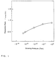
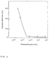
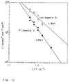
- Fig. 1 illustrates the speed of formation of the film on the silicon electrode at the respective pressures. Examination of this drawing reveals that the film formation speed increases somewhat as the pressure increases. However, the film formation speed increases to approximately twice at most with a change in the pressure by three orders of magnitude.
- Fig. 5(c) shows the shapes of electrodes prepared by formation of a film using a vertical LPCVD apparatus at 560°C for 45 minutes, followed by annealing in a high vacuum for 40 minutes.
- a vertical LPCVD apparatus at 560°C for 45 minutes, followed by annealing in a high vacuum for 40 minutes.
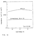
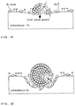
- larger grains were formed on the electrode surfaces since the cylinder electrodes had become thicker.
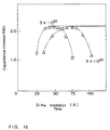
- the result of investigation of the amount of the stored charge with the electrodes was that the amount was 2.2 times that with conventional cylindrical electrodes.
- this process may be utilized in cases where silane gas is used, but cannot be utilized if disilane gas is used. This is because applicable of disilane gas to electrodes of amorphous silicon results in deposition of a poly-crystal film.
- the grains on the surface of the amorphous silicon grow through the process wherein the atoms migrating on the film surface are captured by the micro-crystal nuclei.
- the shapes of the grains shown in Fig. 6 suggest that the dent sections along the peripheries of the grains and the HSG-Si have almost the same volume.
- the process of growth changes depending on the geometries of the grains. Being hemispheric, the grains grow with a proportional relationship between r 2 and the time t.
- the grains grow as spheres, as detailed in Example 2.
- r 3 increases with the time t.
- P atom concentration is lowered near the surface during the growth of the HSG-Si
- Possible reasons why the P atom concentration is lowered near the surface during the growth of the HSG-Si include the process of diffusion of the P into the amorphous silicon or the process of desorption of the P atoms on the film surface. If the P atoms on the film surface diffuse into the inside of the film, then the diffusion may surely be confirmed as change in the P concentration inside the film.
- the grains are hard to take in the P atoms immediately after the formation of the HSG-Si on the surface of P-doped amorphous silicon (P: 1 x 10 20 (atoms/cm 3 )).
- P P-doped amorphous silicon
- the use as a device cannot be realized in practice since a depletion layer is formed in the storage electrode of the capacitor.
- results of EDX analysis of the P concentrations of the grains after formation of the storage electrode have revealed that 5 x 10 19 (atoms/cm 3 ) of P are taken by the grains. This suggests that the P diffuses from the inside of the P-doped amorphous silicon into the grains by passing the process of formation of the capacitor.
- the temperature of the process of formation of the capacitor is approximately 800°C, higher as compared with the temperature for the formation of the grains on the P-doped amorphous silicon (approximately 550°C). It is supposed that the P diffused into the grains by being subjected to this thermal treatment.
- the results of the EDX prove that the P concentrations gradually decrease toward the film surface, starting at a depth of approximately 10 nm from the surface in cases where the surface of the P-doped amorphous silicon film having a P concentration of 1 x 10 20 atoms/cm 3 is treated for the formation of HSG-Si. This suggests that the P atoms diffuse in the amorphous silicon on the order of 500°C and the P atoms are desorbed upon reaching the surface.
- the TDS analysis is a method for analysis of the gas which is desorbed from P-doped amorphous silicon when the film is heated at a given temperature-rise rate.
- the reason for no formation of HSG-Si on the P-doped amorphous silicon having a P concentration of 5 x 10 20 atoms/cm 3 is the temperature for the desorption of the P 2 molecules which is higher than the temperature for the formation of HSG-Si, for which the P has been precipitated on the surface of the amorphous silicon at temperatures within the range of temperatures for forming the HSG-Si.
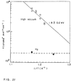
- desorption of the P as P atom at approximately 500°C is the rate-determining process in the formation of the HSG-Si.
- the process of desorption of the P from the film surface at temperatures within the range of temperatures for forming the HSG-Si becomes the rate-determining process in the migration of the silicon atoms which is required for the growth of the HSG-Si.
- the flow rate f of silicon atoms supplied to grains on a P-doped amorphous silicon film is determined by desorption of the P.
- the P-doped amorphous silicon film was formed by an LPCVD method using silane gas and PH 3 gas. Accordingly, the concentration distribution of P in the film prior to the formation of HSG-Si is uniform. This means that the rate-determining factor P in the formation of the HSG-Si is distributed uniformly in the film. Since only the film surface is terminated with hydrogen on the non-doped amorphous silicon, the process of production of the silicon atoms which migrate only on the film surface was influenced by the desorption of the hydrogen.
- the activation energy for the growth of micro-crystals on P-doped amorphous silicon is believed to be the sum of the diffusion and desorption energies of the P in the P-doped amorphous silicon. Based on the thickness of the layer near the surface of the P-doped amorphous silicon which has a lower P concentration, the migration length of the P is believed to be on the order of 10 nm.
- micro-crystal nuclei As mentioned above, irradiation with silane gas alone fails to directly deposit micro-crystal nuclei on P-doped amorphous silicon.
- growing of a non-doped amorphous silicon on the P-doped silicon causes lowering in the P concentration of the film surface and desorption of the P from the film surface.
- the silicon atoms migrate on the surface due to the thermal energy, and micro-crystal nuclei are formed on the film surface. The silicon atoms are captured by these micro-crystal nuclei, and the micro-crystals grow in this way.
- the volume increase ratio falls if the silane gas irradiation process is carried out over a prolonged period. This is because, as will be indicated in Embodiment 4 given below, the grain size is decreased.
- the volume increase ratio is prevented from falling by formation of micro-crystals of relatively large size through irradiation with oxygen in 5 minutes after the start of the annealing. Details thereof will be described in Example 5 given below.
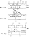
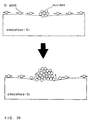
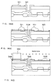
- amorphous silicon layer doped with phosphorus is deposited over the entire surface, followed by being etched-back until the surfaces of the insulating layers 410 are exposed. By removing the insulating layers 410, cylinder-type amorphous silicon electrodes 450 doped with impurities are formed as shown in Fig. 22(b).
- each cylinder electrode 450 is then cleaned to remove a natural silicon oxide film therefrom, and thereafter, a relatively thick, non-doped amorphous silicon film is deposited on each electrode 450, followed by performing annealing process in an inert gas in such a manner as described above.
- cylindrical silicon electrodes 460 are formed with an uneven surface caused by the hemispherical or spherical silicon grains, as shown in Fig. 22(c).
- dielectric films 470 are formed in the same way as described with reference to Fig. 21(e), and a cell plate electrode layer 480 is deposited thereover, as also shown in Fig. 22(c).
- the provision is accomplished when hydrogen is applied, since the surface migration of the silicon atoms is suppressed. Contrary, in the case of irradiation of oxygen, the surface migration of the silicon atoms on the surface of the silicon film is suppressed since approximately one atom layer of the film surface is oxidized.
- a silicon film with a smooth surface is formed by decreasing the temperature in the course of the treatment.
- a UHV-CVD (Ultra High Vacuum Chemical Vapor Deposition) apparatus (SRE612 manufactured by ANEL VA) was used for the formation of HSG-Si. Air was exhausted from the growth chamber to a degree of vacuum of 8.5 x 10 -10 Torr with a turbo-molecular pump. The inside wall of the growth chamber is cooled, and the heating mechanism section and the reaction chamber are separated from each other by the substrate itself. This configuration prevents a decomposition reaction of the gas in portions other than the substrate. Heating of the wafer was accomplished by thermal radiation from a carbon heater. Irradiation with disilane gas and annealing treatment for the formation of HSG-Si were conducted continuously in the growth chamber.
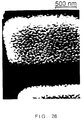
- HSG-Si is densely formed also on the side surface of the electrode in the same manner as on the top surface thereof. It is also found that no nuclei are formed on the oxide film, and HSG-Si is formed on the electrode of amorphous silicon.
- Fig. 27 illustrates the state of growth of the grains when annealed in a high vacuum or in hydrogen (H 2 ).
- H 2 hydrogen
- the same drawing shows that growth of grains does not occur on the amorphous silicon film annealed in hydrogen gas.
- the growth of grains was observed when annealed in nitrogen gas, in the same manner as in the case of the annealing in a high vacuum.
- the above-mentioned facts suggest that hydrogen works as the factor in completely preventing the growth of the grains.
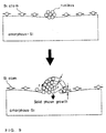
- Fig. 29 is a schematic view illustrative of the typical process of growth of the HSG-Si formed by annealing, in a high vacuum, amorphous silicon with a clean surface.
- the same drawing shows the process of growth of a grain on amorphous silicon which is not terminated with hydrogen.
- a grain grows as indicated by the arrow through capture of silicon atoms (Si atoms) migrating on the surface by a nucleus formed on the amorphous silicon (amorphous-Si). That is, HSG-Si grows around the nucleus.
- the silicon to be used up for the growth of the HSG-Si is made up for by supply from the amorphous silicon surrounding the grain.
- Equation (2) to Equation (4) which regulate the growth of each grain, advances gradually after the size of each grain has attained 50 nm or more. This process will be discussed later.
- the production of the silicon which migrates determines the rate
- the number of the silicon atoms supplied to each grain should increase as the area of the dent section along the perimeter of each grain increases.
- the flow rate f of the silicon supplied to each grain is constant regardless of the area of each section for producing the silicon atoms which migrate. This suggests that during the formation of the spheric grains the process of production of the silicon which migrates does not determine the rate of the growth of the grains.
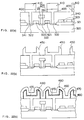
- the photoresist layer is then removed, and the exposed part of the poly-silicon layer 521 is cleaned in a manner as described above to remove a native oxide film therefrom.
- a amorphous silicon layer is then deposited over the entire surface by LPCVD using a silane gas in a thickness of 15 nm.
- the flow rate of the silane gas is 200 cc/min in an vacuum atmosphere of 0.1 Torr.
- a hydrogen gas is introduced at a pressure of 1 Torr, and an annealing is performed at a temperature of 600°C for three hours.
- N-type impurities such as arsenic are then implanted, followed by annealing and patterning.
- N-type impurities-doped poly-silicon layers 531 is formed as shown in Fig. 34(e).
- an interlayer insulating film 553 is deposited over the entire surface, followed by forming a bit contact hole 554.
- a bit line 559 is thereafter formed with filling the contact hole 554.
Landscapes
- Engineering & Computer Science (AREA)
- Manufacturing & Machinery (AREA)
- Semiconductor Memories (AREA)
- Formation Of Insulating Films (AREA)
- Electrodes Of Semiconductors (AREA)
- Semiconductor Integrated Circuits (AREA)
- Chemical Vapour Deposition (AREA)
- Photovoltaic Devices (AREA)
Applications Claiming Priority (6)
| Application Number | Priority Date | Filing Date | Title |
|---|---|---|---|
| JP72276/95 | 1995-03-06 | ||
| JP7227695 | 1995-03-06 | ||
| JP7227695 | 1995-03-06 | ||
| JP28448595 | 1995-10-05 | ||
| JP7284485A JP2833545B2 (ja) | 1995-03-06 | 1995-10-05 | 半導体装置の製造方法 |
| JP284485/95 | 1995-10-05 |
Publications (2)
| Publication Number | Publication Date |
|---|---|
| EP0731491A2 true EP0731491A2 (de) | 1996-09-11 |
| EP0731491A3 EP0731491A3 (de) | 2000-09-06 |
Family
ID=26413416
Family Applications (1)
| Application Number | Title | Priority Date | Filing Date |
|---|---|---|---|
| EP96103418A Withdrawn EP0731491A3 (de) | 1995-03-06 | 1996-03-05 | Verfahren zur Herstellung einer Silizium-Schicht mit einer Oberfläche von kontrollierter Ebenheit bzw. Unebenheit |
Country Status (5)
| Country | Link |
|---|---|
| US (2) | US5910019A (de) |
| EP (1) | EP0731491A3 (de) |
| JP (1) | JP2833545B2 (de) |
| KR (1) | KR100221755B1 (de) |
| TW (2) | TW376545B (de) |
Cited By (7)
| Publication number | Priority date | Publication date | Assignee | Title |
|---|---|---|---|---|
| GB2327299A (en) * | 1997-07-15 | 1999-01-20 | Nec Corp | Method of manufacturing silicon hemispherical grains |
| EP0902462A1 (de) * | 1997-09-08 | 1999-03-17 | Samsung Electronics Co., Ltd. | Verfahren zur Herstellung einer Unterelektrode für eine Halbleiterspeichervorrichtung |
| US5960281A (en) * | 1996-05-23 | 1999-09-28 | Samsung Electronics Co., Ltd. | Methods of fabricating microelectronic electrode structures using hemispherical grained (HSG) silicon |
| GB2341725A (en) * | 1998-08-28 | 2000-03-22 | Samsung Electronics Co Ltd | Method for fabricating a capacitor utilizing hemispherical grain silicon |
| US6245632B1 (en) | 1997-05-22 | 2001-06-12 | Samsung Electronics Co., Ltd. | Variable temperature methods of forming hemispherical grained silicon (HSG-Si) layers |
| EP1455384A3 (de) * | 1997-09-10 | 2004-10-20 | Samsung Electronics Co., Ltd. | Eine Vorrichtung zur Herstellung von einem Halbleiter-Bauelement und ein diesen Vorrichtung verwendenden Verfahren zur Herstellung einer Polysilizium-Schicht |
| US8945962B2 (en) | 2007-10-05 | 2015-02-03 | Semiconductor Energy Laboratory Co., Ltd. | Thin film transistor, display device having thin film transistor, and method for manufacturing the same |
Families Citing this family (45)
| Publication number | Priority date | Publication date | Assignee | Title |
|---|---|---|---|---|
| JP3070660B2 (ja) * | 1996-06-03 | 2000-07-31 | 日本電気株式会社 | 気体不純物の捕獲方法及び半導体製造装置 |
| KR100281979B1 (ko) * | 1997-03-19 | 2001-03-02 | 황철주 | 반도체웨이퍼세정방법및산화막형성방법 |
| JP2982739B2 (ja) * | 1997-04-22 | 1999-11-29 | 日本電気株式会社 | 半導体装置の製造方法 |
| JP3024589B2 (ja) | 1997-04-23 | 2000-03-21 | 日本電気株式会社 | 半導体装置の製造方法 |
| US6255159B1 (en) | 1997-07-14 | 2001-07-03 | Micron Technology, Inc. | Method to form hemispherical grained polysilicon |
| JP3159136B2 (ja) * | 1997-07-18 | 2001-04-23 | 日本電気株式会社 | 半導体装置の製造方法 |
| JP3180740B2 (ja) | 1997-11-11 | 2001-06-25 | 日本電気株式会社 | キャパシタの製造方法 |
| JPH11162876A (ja) | 1997-11-28 | 1999-06-18 | Nec Corp | 半導体装置の製造装置及び製造方法 |
| JPH11233735A (ja) | 1998-02-16 | 1999-08-27 | Nec Corp | 下部電極構造、それを用いたキャパシタ及びその形成方法 |
| JP3244049B2 (ja) * | 1998-05-20 | 2002-01-07 | 日本電気株式会社 | 半導体装置の製造方法 |
| JP3468347B2 (ja) * | 1998-06-22 | 2003-11-17 | 日本エー・エス・エム株式会社 | 半導体素子の製造方法 |
| JP2000012783A (ja) * | 1998-06-22 | 2000-01-14 | Nippon Asm Kk | 半導体素子の製造方法 |
| KR100290835B1 (ko) * | 1998-06-23 | 2001-07-12 | 윤종용 | 반도체소자의제조방법 |
| US6127221A (en) * | 1998-09-10 | 2000-10-03 | Vanguard International Semiconductor Corporation | In situ, one step, formation of selective hemispherical grain silicon layer, and a nitride-oxide dielectric capacitor layer, for a DRAM application |
| US6291294B1 (en) * | 1998-10-13 | 2001-09-18 | Taiwan Semiconductor Manufacturing Corporation | Method for making a stack bottom storage node having reduced crystallization of amorphous polysilicon |
| JP3125770B2 (ja) * | 1998-11-11 | 2001-01-22 | 日本電気株式会社 | 容量素子の形成方法 |
| US6959384B1 (en) * | 1999-12-14 | 2005-10-25 | Intertrust Technologies Corporation | Systems and methods for authenticating and protecting the integrity of data streams and other data |
| KR100587046B1 (ko) * | 2000-05-31 | 2006-06-07 | 주식회사 하이닉스반도체 | 반도체 소자의 전하저장 전극 제조 방법 |
| US6406981B1 (en) * | 2000-06-30 | 2002-06-18 | Intel Corporation | Method for the manufacture of semiconductor devices and circuits |
| US6743697B2 (en) | 2000-06-30 | 2004-06-01 | Intel Corporation | Thin silicon circuits and method for making the same |
| US7237125B2 (en) * | 2000-08-28 | 2007-06-26 | Contentguard Holdings, Inc. | Method and apparatus for automatically deploying security components in a content distribution system |
| AUPQ975900A0 (en) * | 2000-08-30 | 2000-09-21 | Unisearch Limited | A process for the fabrication of a quantum computer |
| JP4876306B2 (ja) * | 2000-10-19 | 2012-02-15 | ソニー株式会社 | 半導体装置の製造方法 |
| KR100347764B1 (ko) * | 2000-10-19 | 2002-08-09 | 삼성전자 주식회사 | 주사전자현미경 이미지를 이용한 반도체 웨이퍼 표면의 입자성장도 수치적 분석방법과 이를 위한 장치 |
| US6459482B1 (en) | 2000-10-24 | 2002-10-01 | Advanced Micro Devices, Inc. | Grainless material for calibration sample |
| JP2003078028A (ja) * | 2001-08-31 | 2003-03-14 | Hitachi Ltd | 半導体装置およびその製造方法 |
| US6746933B1 (en) * | 2001-10-26 | 2004-06-08 | International Business Machines Corporation | Pitcher-shaped active area for field effect transistor and method of forming same |
| US6887755B2 (en) * | 2003-09-05 | 2005-05-03 | Micron Technology, Inc. | Methods of forming rugged silicon-containing surfaces |
| US7341907B2 (en) * | 2005-04-05 | 2008-03-11 | Applied Materials, Inc. | Single wafer thermal CVD processes for hemispherical grained silicon and nano-crystalline grain-sized polysilicon |
| US20060276038A1 (en) * | 2005-06-03 | 2006-12-07 | Pun Arthur F | Thermal desorption of oxide from surfaces |
| JP2007053279A (ja) * | 2005-08-19 | 2007-03-01 | Elpida Memory Inc | 半導体装置の製造方法 |
| KR100691958B1 (ko) * | 2005-10-13 | 2007-03-09 | 동부일렉트로닉스 주식회사 | 반도체 소자의 제조 방법 |
| US20080227267A1 (en) * | 2007-03-14 | 2008-09-18 | Theodorus Gerardus Maria Oosterlaken | Stop mechanism for trench reshaping process |
| KR101455304B1 (ko) * | 2007-10-05 | 2014-11-03 | 가부시키가이샤 한도오따이 에네루기 켄큐쇼 | 박막트랜지스터, 및 박막트랜지스터를 가지는 표시장치, 및그들의 제작방법 |
| JP5311957B2 (ja) * | 2007-10-23 | 2013-10-09 | 株式会社半導体エネルギー研究所 | 表示装置及びその作製方法 |
| JP5311955B2 (ja) * | 2007-11-01 | 2013-10-09 | 株式会社半導体エネルギー研究所 | 表示装置の作製方法 |
| KR101610260B1 (ko) * | 2008-12-15 | 2016-04-08 | 삼성전자주식회사 | 전자빔 어닐링 장치 및 이를 이용한 어닐링 방법 |
| US8263988B2 (en) | 2010-07-16 | 2012-09-11 | Micron Technology, Inc. | Solid state lighting devices with reduced crystal lattice dislocations and associated methods of manufacturing |
| KR20120064364A (ko) * | 2010-12-09 | 2012-06-19 | 삼성전자주식회사 | 태양 전지의 제조 방법 |
| US8669184B2 (en) * | 2011-01-24 | 2014-03-11 | Macronix International Co., Ltd. | Method for improving flatness of a layer deposited on polycrystalline layer |
| CN103681244B (zh) * | 2013-12-25 | 2016-09-14 | 深圳市华星光电技术有限公司 | 低温多晶硅薄膜的制备方法及其制作系统 |
| US9837271B2 (en) | 2014-07-18 | 2017-12-05 | Asm Ip Holding B.V. | Process for forming silicon-filled openings with a reduced occurrence of voids |
| US9443730B2 (en) | 2014-07-18 | 2016-09-13 | Asm Ip Holding B.V. | Process for forming silicon-filled openings with a reduced occurrence of voids |
| JP6545093B2 (ja) * | 2015-12-14 | 2019-07-17 | 株式会社Kokusai Electric | 半導体装置の製造方法、基板処理装置およびプログラム |
| US10460932B2 (en) | 2017-03-31 | 2019-10-29 | Asm Ip Holding B.V. | Semiconductor device with amorphous silicon filled gaps and methods for forming |
Family Cites Families (10)
| Publication number | Priority date | Publication date | Assignee | Title |
|---|---|---|---|---|
| US4497683A (en) * | 1982-05-03 | 1985-02-05 | At&T Bell Laboratories | Process for producing dielectrically isolated silicon devices |
| KR900007686B1 (ko) * | 1986-10-08 | 1990-10-18 | 후지쓰 가부시끼가이샤 | 선택적으로 산화된 실리콘 기판상에 에피택셜 실리콘층과 다결정 실리콘층을 동시에 성장시키는 기상 증착방법 |
| US4965225A (en) * | 1988-09-30 | 1990-10-23 | Kanegafuchi Chemical Industry Co., Ltd. | Method of stabilizing amorphous semiconductors |
| JP2894361B2 (ja) * | 1990-02-16 | 1999-05-24 | 三菱電機株式会社 | 半導体装置およびその製造方法 |
| JP2937395B2 (ja) * | 1990-03-20 | 1999-08-23 | 日本電気株式会社 | 半導体素子 |
| US5147826A (en) * | 1990-08-06 | 1992-09-15 | The Pennsylvania Research Corporation | Low temperature crystallization and pattering of amorphous silicon films |
| JP2508948B2 (ja) * | 1991-06-21 | 1996-06-19 | 日本電気株式会社 | 半導体装置の製造方法 |
| JP3159796B2 (ja) * | 1992-07-24 | 2001-04-23 | 宮崎沖電気株式会社 | 半導体素子の製造方法 |
| JPH06163850A (ja) * | 1992-11-25 | 1994-06-10 | Nec Corp | 半導体装置の製造方法 |
| EP0678907B1 (de) * | 1994-04-22 | 2002-02-27 | Nec Corporation | Methode zur Herstellung eines Dünnfilm-Transistors mit invertierter Struktur |
-
1995
- 1995-10-05 JP JP7284485A patent/JP2833545B2/ja not_active Expired - Fee Related
-
1996
- 1996-03-05 TW TW085114573A patent/TW376545B/zh not_active IP Right Cessation
- 1996-03-05 EP EP96103418A patent/EP0731491A3/de not_active Withdrawn
- 1996-03-05 TW TW085102682A patent/TW368695B/zh not_active IP Right Cessation
- 1996-03-06 KR KR1019960006282A patent/KR100221755B1/ko not_active Expired - Fee Related
-
1997
- 1997-04-02 US US08/829,358 patent/US5910019A/en not_active Expired - Lifetime
- 1997-09-08 US US08/926,408 patent/US5989969A/en not_active Expired - Lifetime
Cited By (10)
| Publication number | Priority date | Publication date | Assignee | Title |
|---|---|---|---|---|
| US5960281A (en) * | 1996-05-23 | 1999-09-28 | Samsung Electronics Co., Ltd. | Methods of fabricating microelectronic electrode structures using hemispherical grained (HSG) silicon |
| US6245632B1 (en) | 1997-05-22 | 2001-06-12 | Samsung Electronics Co., Ltd. | Variable temperature methods of forming hemispherical grained silicon (HSG-Si) layers |
| GB2327299A (en) * | 1997-07-15 | 1999-01-20 | Nec Corp | Method of manufacturing silicon hemispherical grains |
| EP0902462A1 (de) * | 1997-09-08 | 1999-03-17 | Samsung Electronics Co., Ltd. | Verfahren zur Herstellung einer Unterelektrode für eine Halbleiterspeichervorrichtung |
| EP1455384A3 (de) * | 1997-09-10 | 2004-10-20 | Samsung Electronics Co., Ltd. | Eine Vorrichtung zur Herstellung von einem Halbleiter-Bauelement und ein diesen Vorrichtung verwendenden Verfahren zur Herstellung einer Polysilizium-Schicht |
| GB2341725A (en) * | 1998-08-28 | 2000-03-22 | Samsung Electronics Co Ltd | Method for fabricating a capacitor utilizing hemispherical grain silicon |
| US6333227B1 (en) | 1998-08-28 | 2001-12-25 | Samsung Electronics Co., Ltd. | Methods of forming hemispherical grain silicon electrodes by crystallizing the necks thereof |
| GB2341725B (en) * | 1998-08-28 | 2003-07-23 | Samsung Electronics Co Ltd | Method for fabricating a capacitor utilizing hemispherical grain silicon |
| DE19929605B4 (de) * | 1998-08-28 | 2006-08-10 | Samsung Electronics Co., Ltd., Suwon | Verfahren zur Herstellung eines Kondensators unter Verwendung von Silizium mit halbkugelförmigen Körnchen |
| US8945962B2 (en) | 2007-10-05 | 2015-02-03 | Semiconductor Energy Laboratory Co., Ltd. | Thin film transistor, display device having thin film transistor, and method for manufacturing the same |
Also Published As
| Publication number | Publication date |
|---|---|
| JP2833545B2 (ja) | 1998-12-09 |
| JPH08306646A (ja) | 1996-11-22 |
| US5989969A (en) | 1999-11-23 |
| TW368695B (en) | 1999-09-01 |
| US5910019A (en) | 1999-06-08 |
| TW376545B (en) | 1999-12-11 |
| EP0731491A3 (de) | 2000-09-06 |
| KR100221755B1 (ko) | 1999-09-15 |
Similar Documents
| Publication | Publication Date | Title |
|---|---|---|
| US5989969A (en) | Method of producing silicon layer having surface controlled to be uneven | |
| EP0521644B1 (de) | Verfahren zur Herstellung eines polykristallinen Siliziumfilmes | |
| JP2701803B2 (ja) | 半導体装置の製造方法 | |
| US20120211824A1 (en) | vertical transistor having a gate structure formed on a buried drain region and a source region overlying the upper most layer of the gate structure | |
| US6159874A (en) | Method of forming a hemispherical grained capacitor | |
| US6620740B2 (en) | Methods to form electronic devices | |
| KR100224707B1 (ko) | 반도체 장치 커패시터의 제조방법 | |
| KR100259038B1 (ko) | 반도체커패시터제조방법및그에따라형성된반도체커패시터 | |
| JP2947828B2 (ja) | 半導体装置の製造方法 | |
| JPH11150249A (ja) | 凹凸状ポリシリコン層の形成方法及びこの方法の実施に使用される基板処理装置並びに半導体メモリデバイス | |
| US6300217B1 (en) | Method for fabricating a semiconductor device including a step for forming an amorphous silicon layer followed by a crystallization thereof | |
| US5858853A (en) | Method for forming capacitor electrode having jagged surface | |
| US6534815B2 (en) | Semiconductor device with stack electrode formed using HSG growth | |
| US5723887A (en) | Semiconductor memory device and manufacturing method thereof | |
| JPH0645521A (ja) | 半導体素子の製造方法 | |
| US6403455B1 (en) | Methods of fabricating a memory device | |
| JPH11274097A (ja) | 半導体装置の製造方法 | |
| US6335242B1 (en) | Method for fabricating semiconductor device having a HSG layer | |
| US20070042574A1 (en) | Method for manufacturing a semiconductor device | |
| US20040005788A1 (en) | Method of forming a silicon nitride dielectric layer | |
| Mansoori et al. | Selective hemispherical grained polysilicon transformation for 256 MB, 1 GB dynamic random access memory and beyond | |
| JP3039532B2 (ja) | 半導体装置の製造方法 | |
| JPH09191092A (ja) | 多結晶シリコン膜の形成方法及びこれを用いた半導体装置のキャパシタの製造方法 | |
| JP3439381B2 (ja) | 半導体装置の製造方法 | |
| KR19990012156A (ko) | 전극들간의 인가전압에 관해 안정된 캐패시턴스를 가지는굴곡형다결정 실리콘 전극상의 고유전체 스토리지 캐패시터및 그 제조방법. |
Legal Events
| Date | Code | Title | Description |
|---|---|---|---|
| PUAI | Public reference made under article 153(3) epc to a published international application that has entered the european phase |
Free format text: ORIGINAL CODE: 0009012 |
|
| AK | Designated contracting states |
Kind code of ref document: A2 Designated state(s): DE FR GB NL |
|
| PUAL | Search report despatched |
Free format text: ORIGINAL CODE: 0009013 |
|
| AK | Designated contracting states |
Kind code of ref document: A3 Designated state(s): DE FR GB NL |
|
| 17P | Request for examination filed |
Effective date: 20000801 |
|
| RAP1 | Party data changed (applicant data changed or rights of an application transferred) |
Owner name: NEC ELECTRONICS CORPORATION |
|
| STAA | Information on the status of an ep patent application or granted ep patent |
Free format text: STATUS: THE APPLICATION HAS BEEN WITHDRAWN |
|
| 18W | Application withdrawn |
Effective date: 20080808 |