EP0732830A2 - Circuit pour la récupération d'horloge d'un train de données à haute vitesse - Google Patents
Circuit pour la récupération d'horloge d'un train de données à haute vitesse Download PDFInfo
- Publication number
- EP0732830A2 EP0732830A2 EP96103852A EP96103852A EP0732830A2 EP 0732830 A2 EP0732830 A2 EP 0732830A2 EP 96103852 A EP96103852 A EP 96103852A EP 96103852 A EP96103852 A EP 96103852A EP 0732830 A2 EP0732830 A2 EP 0732830A2
- Authority
- EP
- European Patent Office
- Prior art keywords
- signal
- supplied
- frequency
- gate
- wire
- Prior art date
- Legal status (The legal status is an assumption and is not a legal conclusion. Google has not performed a legal analysis and makes no representation as to the accuracy of the status listed.)
- Withdrawn
Links
- 238000000605 extraction Methods 0.000 title claims abstract description 9
- 230000000295 complement effect Effects 0.000 claims description 6
- 238000005070 sampling Methods 0.000 claims description 4
- 230000007704 transition Effects 0.000 claims description 3
- 238000010586 diagram Methods 0.000 description 8
- 238000012937 correction Methods 0.000 description 5
- 230000010355 oscillation Effects 0.000 description 5
- 238000005259 measurement Methods 0.000 description 2
- 230000001360 synchronised effect Effects 0.000 description 2
- 230000005540 biological transmission Effects 0.000 description 1
- 239000013078 crystal Substances 0.000 description 1
- 238000001514 detection method Methods 0.000 description 1
- 230000000694 effects Effects 0.000 description 1
- 230000002349 favourable effect Effects 0.000 description 1
- 238000000034 method Methods 0.000 description 1
- 238000012986 modification Methods 0.000 description 1
- 230000004048 modification Effects 0.000 description 1
- 239000010453 quartz Substances 0.000 description 1
- 230000008054 signal transmission Effects 0.000 description 1
- VYPSYNLAJGMNEJ-UHFFFAOYSA-N silicon dioxide Inorganic materials O=[Si]=O VYPSYNLAJGMNEJ-UHFFFAOYSA-N 0.000 description 1
Images
Classifications
-
- H—ELECTRICITY
- H03—ELECTRONIC CIRCUITRY
- H03L—AUTOMATIC CONTROL, STARTING, SYNCHRONISATION OR STABILISATION OF GENERATORS OF ELECTRONIC OSCILLATIONS OR PULSES
- H03L7/00—Automatic control of frequency or phase; Synchronisation
- H03L7/06—Automatic control of frequency or phase; Synchronisation using a reference signal applied to a frequency- or phase-locked loop
- H03L7/08—Details of the phase-locked loop
- H03L7/14—Details of the phase-locked loop for assuring constant frequency when supply or correction voltages fail
-
- H—ELECTRICITY
- H03—ELECTRONIC CIRCUITRY
- H03L—AUTOMATIC CONTROL, STARTING, SYNCHRONISATION OR STABILISATION OF GENERATORS OF ELECTRONIC OSCILLATIONS OR PULSES
- H03L7/00—Automatic control of frequency or phase; Synchronisation
- H03L7/06—Automatic control of frequency or phase; Synchronisation using a reference signal applied to a frequency- or phase-locked loop
- H03L7/08—Details of the phase-locked loop
- H03L7/10—Details of the phase-locked loop for assuring initial synchronisation or for broadening the capture range
- H03L7/113—Details of the phase-locked loop for assuring initial synchronisation or for broadening the capture range using frequency discriminator
-
- H—ELECTRICITY
- H04—ELECTRIC COMMUNICATION TECHNIQUE
- H04L—TRANSMISSION OF DIGITAL INFORMATION, e.g. TELEGRAPHIC COMMUNICATION
- H04L7/00—Arrangements for synchronising receiver with transmitter
- H04L7/02—Speed or phase control by the received code signals, the signals containing no special synchronisation information
- H04L7/033—Speed or phase control by the received code signals, the signals containing no special synchronisation information using the transitions of the received signal to control the phase of the synchronising-signal-generating means, e.g. using a phase-locked loop
-
- H—ELECTRICITY
- H03—ELECTRONIC CIRCUITRY
- H03D—DEMODULATION OR TRANSFERENCE OF MODULATION FROM ONE CARRIER TO ANOTHER
- H03D13/00—Circuits for comparing the phase or frequency of two mutually-independent oscillations
- H03D13/003—Circuits for comparing the phase or frequency of two mutually-independent oscillations in which both oscillations are converted by logic means into pulses which are applied to filtering or integrating means
- H03D13/004—Circuits for comparing the phase or frequency of two mutually-independent oscillations in which both oscillations are converted by logic means into pulses which are applied to filtering or integrating means the logic means delivering pulses at more than one terminal, e.g. up and down pulses
-
- H—ELECTRICITY
- H03—ELECTRONIC CIRCUITRY
- H03L—AUTOMATIC CONTROL, STARTING, SYNCHRONISATION OR STABILISATION OF GENERATORS OF ELECTRONIC OSCILLATIONS OR PULSES
- H03L7/00—Automatic control of frequency or phase; Synchronisation
- H03L7/06—Automatic control of frequency or phase; Synchronisation using a reference signal applied to a frequency- or phase-locked loop
- H03L7/08—Details of the phase-locked loop
- H03L7/085—Details of the phase-locked loop concerning mainly the frequency- or phase-detection arrangement including the filtering or amplification of its output signal
- H03L7/087—Details of the phase-locked loop concerning mainly the frequency- or phase-detection arrangement including the filtering or amplification of its output signal using at least two phase detectors or a frequency and phase detector in the loop
-
- H—ELECTRICITY
- H03—ELECTRONIC CIRCUITRY
- H03L—AUTOMATIC CONTROL, STARTING, SYNCHRONISATION OR STABILISATION OF GENERATORS OF ELECTRONIC OSCILLATIONS OR PULSES
- H03L7/00—Automatic control of frequency or phase; Synchronisation
- H03L7/06—Automatic control of frequency or phase; Synchronisation using a reference signal applied to a frequency- or phase-locked loop
- H03L7/08—Details of the phase-locked loop
- H03L7/085—Details of the phase-locked loop concerning mainly the frequency- or phase-detection arrangement including the filtering or amplification of its output signal
- H03L7/089—Details of the phase-locked loop concerning mainly the frequency- or phase-detection arrangement including the filtering or amplification of its output signal the phase or frequency detector generating up-down pulses
- H03L7/0891—Details of the phase-locked loop concerning mainly the frequency- or phase-detection arrangement including the filtering or amplification of its output signal the phase or frequency detector generating up-down pulses the up-down pulses controlling source and sink current generators, e.g. a charge pump
Definitions
- the present invention relates to apparatus for digital signal transmission between electronic systems located at some distance from one another and in particular it concerns a circuit for clock signal extraction from a high speed data stream.
- a receiving device must have at disposal a clock signal that is exactly synchronised with the incoming digital stream, so as to be able to evaluate the logic levels in the most favourable instants.
- the data signal is transmitted with an associated clock signal, in particular when transmission is performed serially on a single line.
- the clock signal for the detection must be recovered by extracting the necessary information from the data signal itself.
- This operation is usually carried out by means of the known PLL (Phase Locked Loop) circuit, by using as a reference signal the digital signal incoming at the receiver to generate an output clock signal whose frequency is equal to the bit rate of the data signal.
- the reconstructed clock signal has a very well defined phase relationship with the data signal, so as to present the low to high level transitions in correspondence with the optimal sampling instant.
- phase locked loop The main components of the phase locked loop are, as is well known, a phase detector, a filter and a Voltage Controlled Oscillator (VCO).
- the detector compares the phase of the data signal with that of the clock signal locally generated by the VCO and supplies an error signal which, through the filter, controls the VCO by continually controlling its phase.
- the circuit for clock signal extraction from a high speed data stream which allows a quick attainment of the identity between the frequency of the locally generated clock signal and that of the data signal, even when such frequencies are very different.
- the circuit can easily be introduced into a more complex CMOS digital integrated circuit: this allows a better engineering of the printed circuit boards, since an external PLL circuit is no longer required.
- the circuit if it is realised in CMOS technology, has low power dissipation and it is capable of operating at bit rates in excess of 300 Mbit/s.
- Particular object of the present invention is to provide a circuit for the extraction of the clock signal from a high speed data stream as claimed in claim 1.
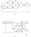
- the circuit for clock signal extraction from a high speed data stream is based on a dual-loop PLL structure.
- the main loop comprising a phase detector DFS, a driven current generator PC1, a loop filter Fl and a voltage controlled oscillator VCO, provides for phase locking the clock signal generated by the VCO, present on wire 2, with the data incoming on wire 1.
- the secondary loop comprising a frequency detector DFR, a threshold comparator CS, a driven current generator PC2, filter Fl and oscillator VCO, is to allow the main loop to become locked by bringing oscillator VCO to oscillate at a frequency close to the desired one.
- frequency detector DFR provides error pulses on wire 4, if the frequency on wire 2 is too low, or on wire 5 if the frequency is too high.
- the frequency of these pulses is proportional to the difference between the frequency present on wire 2 and four times the one present on wire 3; moreover, in the case of a large difference, for instance exceeding 25%, not only the frequency but also the duration of the pulses is proportional to that difference.
- the overall effect is to make the mean value of the error signal proportional to the frequency difference.
- Threshold comparator CS operates in such a way as to let error pulses on wires 4 or 5 pass to wires 6 or 7, respectively, only if their frequency exceeds a pre-set value; otherwise comparator CS blocks the pulses.
- Driven current generator PC2 supplies a pre-set amount of charge to filter Fl in response to a pulse on wire 6, whilst it removes the same amount of charge in the presence of a pulse on wire 7.
- Filter Fl composed of a resistance-capacitance (RC) network, as a result varies the voltage on wire 12, which voltage controls the oscillating frequency of VCO and approximates it to the desired one.
- RC resistance-capacitance
- the frequency of the pulses exiting DFR becomes lower than the threshold of comparator CS, which as a result prevents the propagation of additional pulses towards driven current generator PC2.
- the secondary loop stops operating and control is assumed by the blocks forming the main loop.
- threshold comparator CS allows the use of a local oscillator that is able to provide a reference signal with a frequency which may differ even up to 0.1% from the one associated with the incoming data, divided by four. Therefore, even a simple, not particularly accurate quartz crystal oscillator could be used, for example.
- Phase detector DFS which belongs to the main loop, compares the phase of the signal generated by VCO, present on wire 2, with that of the data signal received on wire 1 and supplies on one of wires 9 or 10 pulses of constant duration and on the other wire pulses whose duration depends on the phase error.
- the net current injected into filter Fl by driven current generator PC1 by means of wire 11 is proportional to the difference in duration of the pulses on the two wires; the resulting voltage variation obtained at the output of filter Fl on wire 12 causes a corresponding frequency variation of the signal on wire 2, which zeroes the phase error.
- Block DFR is represented in detail in the block diagram in Figure 2.
- Frequency detector DFR operates synchronously with the input reference signal present on wire 3, whose frequency is equal to a quarter of the one to be imposed on the signal present on wire 2.
- the choice of a quarter is linked with the particular embodiment, but by suitably adapting the modules forming the structure, the ratio of the input frequencies could have any value.
- the frequency of the signal on wire 2 is divided by 16 by a divider D1, whose output signal on wire 22 is sampled by a sampling block S1, essentially comprising a flip-flop controlled by the signal on wire 3.
- the signal at the output of block S1 on wire 23, which is thus synchronised, is supplied to a subsequent divider D2, which divides said signal preferably by two, thereby supplying pulses at stable logic level on wire 24.
- blocks M1, PU1 and PD1 are to generate correction pulses starting from the measurement of the duration of logic level "1" on wire 24; the purpose of blocks M2, PU2, PD2 is to generate correction pulses starting from the measurement of the duration of logic level "1" on wire 25, which level corresponds to logic level "0" on wire 24, since an inverter 11 is interposed.
- block M1 which consists of a monostable circuit, generates on wire 26 a pulse at logic level "1" of a duration equal to the duration the pulse on wire 24 should have if the oscillation frequency of VCO ( Figure 1) were the desired one.
- the duration of the pulse on wire 26 is determined on the basis of the reference signal on wire 3, while the beginning of the pulse is controlled by the signal on wire 24.
- AND gate PU1 which receives at its inputs the signal on wire 24 and the complement of the signal on wire 26, detects this difference in duration supplying on wire 28 a pulse whose duration is equal to the difference itself. This latter pulse, arriving at wire 4 through OR gate PU3, contributes to raise the oscillation frequency of the signal on wire 2.
- AND gate PD1 which receives at its inputs the complement of the signal on wire 24 and the signal on wire 26, detects this difference in duration, supplying on wire 29 a pulse whose duration is equal to the difference itself. That pulse, arriving at wire 5 through OR gate PD3, contributes to lower the oscillation frequency of the signal on wire 2.
- monostable circuit M2 together with AND gates PU2 and PD2, carries out the same corrections by evaluating the duration of logic level "1" on wire 25, obtained by inverting the signal on wire 24 by means of l1.
- the pulse intended to increasing the oscillation frequency of the signal on wire 2 is supplied by PU2 on wire 30 and it passes to wire 4 through OR gate PU3, whilst the pulse intended to decrease said frequency is supplied by PD2 on wire 31 and it passes on wire 5 through OR gate PD3.
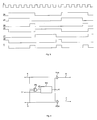
- Figure 3 depicts a time diagram related to the operation of frequency detector DFR.
- every waveform is indicated by the same reference number used to identify the related wire in the previous Figures.
- the example shown refers to a situation in which the oscillation frequency at the output of the VCO is lower than the operating frequency.
- the correction pulses present on wire 4 would maintain the same duration but would be less frequent in time.
- Figure 4 illustrates the block diagram of threshold comparator CS.
- CS is to disable correction by frequency detector DFR ( Figure 1) when the oscillating frequency at the output of the VCO has entered the range of the main loop carrying out the phase locking. Conversely, as soon as the difference in frequency exceeds a pre-defined value, the threshold comparator will enable again the secondary loop operation.
- the main element of the detector is block M3 which, in the presence of an incoming pulse on wire 40, supplies on wire 41 a pulse whose duration is equal to a number N of cycles of the incoming clock signal on wire 3, for example 256 cycles.
- the signal on wire 41 causes gates PU4 and PD4 to open and close, thereby enabling and disabling secondary loop operation. If an incoming pulse arrives on wire 40 while the signal on wire 41 is active, then the duration of the pulse on wire 41 is increased in order to keep the pulse active for N cycles starting from the last pulse that has arrived.
- a pulse on wire 4, or on wire 5 passes through OR gate P4 enabling operation of block M3, which enables the opening of the two gates PU4 and PD4.
- a subsequent pulse on wire 4, or on wire 5, can be transferred through gate PU4 or PD4, respectively, to wire 6 or 7, if it arrives within the enabling interval provided by the signal on wire 41, otherwise it is blocked.
Landscapes
- Engineering & Computer Science (AREA)
- Computer Networks & Wireless Communication (AREA)
- Signal Processing (AREA)
- Stabilization Of Oscillater, Synchronisation, Frequency Synthesizers (AREA)
- Synchronisation In Digital Transmission Systems (AREA)
- Logic Circuits (AREA)
- Manipulation Of Pulses (AREA)
Applications Claiming Priority (2)
| Application Number | Priority Date | Filing Date | Title |
|---|---|---|---|
| ITTO950190 | 1995-03-14 | ||
| IT95TO000190A IT1279165B1 (it) | 1995-03-14 | 1995-03-14 | Circuito per l'estrazione del segnale di orologio da un flusso dati ad alta velocita'. |
Publications (2)
| Publication Number | Publication Date |
|---|---|
| EP0732830A2 true EP0732830A2 (fr) | 1996-09-18 |
| EP0732830A3 EP0732830A3 (fr) | 1999-05-06 |
Family
ID=11413351
Family Applications (1)
| Application Number | Title | Priority Date | Filing Date |
|---|---|---|---|
| EP96103852A Withdrawn EP0732830A3 (fr) | 1995-03-14 | 1996-03-12 | Circuit pour la récupération d'horloge d'un train de données à haute vitesse |
Country Status (6)
| Country | Link |
|---|---|
| US (1) | US5686849A (fr) |
| EP (1) | EP0732830A3 (fr) |
| JP (1) | JP2847493B2 (fr) |
| CA (1) | CA2171690C (fr) |
| DE (1) | DE732830T1 (fr) |
| IT (1) | IT1279165B1 (fr) |
Cited By (4)
| Publication number | Priority date | Publication date | Assignee | Title |
|---|---|---|---|---|
| EP0881773A1 (fr) * | 1997-05-30 | 1998-12-02 | Sun Microsystems, Inc. | Détecteur de différence de fréquence pour un signal NRZ |
| GB2360152A (en) * | 2000-03-10 | 2001-09-12 | Rover Group | Control circuit arrangements |
| EP1912333A1 (fr) * | 2003-12-12 | 2008-04-16 | QUALCOMM Incorporated | Boucle à verrouillage de phase qui règle automatiquement le gain |
| US7825706B2 (en) | 2002-06-28 | 2010-11-02 | Qualcomm Incorporated | Phase locked loop that sets gain automatically |
Families Citing this family (6)
| Publication number | Priority date | Publication date | Assignee | Title |
|---|---|---|---|---|
| JP3407197B2 (ja) | 1999-11-26 | 2003-05-19 | 松下電器産業株式会社 | PLL(PhaseLockedLoop)回路 |
| KR100680476B1 (ko) * | 2000-06-30 | 2007-02-08 | 매그나칩 반도체 유한회사 | 차동 주파수 전류 변환기를 구비한 위상고정루프 |
| US6987824B1 (en) * | 2000-09-21 | 2006-01-17 | International Business Machines Corporation | Method and system for clock/data recovery for self-clocked high speed interconnects |
| JP3968525B2 (ja) * | 2004-03-04 | 2007-08-29 | ソニー株式会社 | 位相同期回路および情報再生装置 |
| US8208596B2 (en) * | 2007-01-17 | 2012-06-26 | Sony Corporation | System and method for implementing a dual-mode PLL to support a data transmission procedure |
| KR102781501B1 (ko) * | 2019-07-18 | 2025-03-17 | 삼성전자주식회사 | 서브 샘플링 pll 회로를 포함하는 pll 회로 및 클록 발생기 |
Family Cites Families (8)
| Publication number | Priority date | Publication date | Assignee | Title |
|---|---|---|---|---|
| US4069462A (en) * | 1976-12-13 | 1978-01-17 | Data General Corporation | Phase-locked loops |
| US4272729A (en) * | 1979-05-10 | 1981-06-09 | Harris Corporation | Automatic pretuning of a voltage controlled oscillator in a frequency synthesizer using successive approximation |
| US4365211A (en) * | 1980-10-31 | 1982-12-21 | Westinghouse Electric Corp. | Phase-locked loop with initialization loop |
| US4787097A (en) * | 1987-02-11 | 1988-11-22 | International Business Machines Corporation | NRZ phase-locked loop circuit with associated monitor and recovery circuitry |
| US5157355A (en) * | 1988-09-13 | 1992-10-20 | Canon Kabushiki Kaisha | Phase-locked loop device having stability over wide frequency range |
| US5015970A (en) * | 1990-02-15 | 1991-05-14 | Advanced Micro Devices, Inc. | Clock recovery phase lock loop having digitally range limited operating window |
| KR950008461B1 (ko) * | 1992-03-18 | 1995-07-31 | 재단법인 한국전자통신연구소 | Nrz 데이터 비트 동기 장치 |
| KR970003097B1 (ko) * | 1994-12-02 | 1997-03-14 | 양승택 | 다단 제어구조를 갖는 고속 비트동기 장치 |
-
1995
- 1995-03-14 IT IT95TO000190A patent/IT1279165B1/it active IP Right Grant
-
1996
- 1996-02-22 US US08/605,393 patent/US5686849A/en not_active Expired - Fee Related
- 1996-03-12 DE DE0732830T patent/DE732830T1/de active Pending
- 1996-03-12 EP EP96103852A patent/EP0732830A3/fr not_active Withdrawn
- 1996-03-13 CA CA002171690A patent/CA2171690C/fr not_active Expired - Fee Related
- 1996-03-14 JP JP8448196A patent/JP2847493B2/ja not_active Expired - Fee Related
Cited By (5)
| Publication number | Priority date | Publication date | Assignee | Title |
|---|---|---|---|---|
| EP0881773A1 (fr) * | 1997-05-30 | 1998-12-02 | Sun Microsystems, Inc. | Détecteur de différence de fréquence pour un signal NRZ |
| US6020765A (en) * | 1997-05-30 | 2000-02-01 | Sun Microsystems, Inc. | Frequency difference detector for use with an NRZ signal |
| GB2360152A (en) * | 2000-03-10 | 2001-09-12 | Rover Group | Control circuit arrangements |
| US7825706B2 (en) | 2002-06-28 | 2010-11-02 | Qualcomm Incorporated | Phase locked loop that sets gain automatically |
| EP1912333A1 (fr) * | 2003-12-12 | 2008-04-16 | QUALCOMM Incorporated | Boucle à verrouillage de phase qui règle automatiquement le gain |
Also Published As
| Publication number | Publication date |
|---|---|
| ITTO950190A1 (it) | 1996-09-14 |
| EP0732830A3 (fr) | 1999-05-06 |
| JPH08279747A (ja) | 1996-10-22 |
| CA2171690C (fr) | 2000-07-18 |
| IT1279165B1 (it) | 1997-12-04 |
| ITTO950190A0 (it) | 1995-03-14 |
| DE732830T1 (de) | 1999-08-19 |
| JP2847493B2 (ja) | 1999-01-20 |
| CA2171690A1 (fr) | 1996-09-15 |
| US5686849A (en) | 1997-11-11 |
Similar Documents
| Publication | Publication Date | Title |
|---|---|---|
| US4789996A (en) | Center frequency high resolution digital phase-lock loop circuit | |
| EP0458269B1 (fr) | Circuit de boucle d'asservissement de phase | |
| JPH0828701B2 (ja) | データ及びクロツク信号回復装置 | |
| US6259326B1 (en) | Clock recovery from a burst-mode digital signal each packet of which may have one of several predefined frequencies | |
| US5276716A (en) | Bi-phase decoder phase-lock loop in CMOS | |
| US6701445B1 (en) | Frequency control system that stabilizes an output through both a counter and voltage-controlled oscillator via sampling a generated clock into four states | |
| US5491729A (en) | Digital phase-locked data recovery circuit | |
| EP0749646B1 (fr) | Circuit processeur d'erreurs de phase avec technique de transfert alternee aux entrees d'un comparateur | |
| WO1987001885A1 (fr) | Circuit detecteur de verrouillage a comparateur de phase et synthetiseur l'utilisant | |
| US5686849A (en) | Circuit for clock signal extraction from a high speed data stream | |
| US5457428A (en) | Method and apparatus for the reduction of time interval error in a phase locked loop circuit | |
| US4661965A (en) | Timing recovery circuit for manchester coded data | |
| US6392495B1 (en) | Frequency detector circuits and systems | |
| US6389090B2 (en) | Digital clock/data signal recovery method and apparatus | |
| KR100265309B1 (ko) | 2상 변조 디지탈 신호로부터의 클럭 신호 발생 방법 및 그 장치 | |
| KR950007435B1 (ko) | 클럭 복원 회로 | |
| RU2138907C1 (ru) | Устройство синхронизации цифрового приемника | |
| KR100290732B1 (ko) | 동기식 직렬 데이타통신 시스템의 클럭 복원방법과 클럭복원회로 | |
| EP0480597A2 (fr) | Dispositif de boucle à verrouillage de phase | |
| EP0404596B1 (fr) | Procédé et appareil de mise en fréquence pour appareil de transmission radio | |
| KR19980019934A (ko) | 멀티위상 클럭을 이용한 클럭/데이터 복원용 피엘엘 | |
| AU674444B2 (en) | Phase detector | |
| US6466635B1 (en) | Process and device for generating a clock signal | |
| JP3810185B2 (ja) | 同期発振回路 | |
| US4642575A (en) | Phase-locked loop with supplemental phase signal |
Legal Events
| Date | Code | Title | Description |
|---|---|---|---|
| PUAI | Public reference made under article 153(3) epc to a published international application that has entered the european phase |
Free format text: ORIGINAL CODE: 0009012 |
|
| AK | Designated contracting states |
Kind code of ref document: A2 Designated state(s): DE FR GB IT NL SE |
|
| PUAL | Search report despatched |
Free format text: ORIGINAL CODE: 0009013 |
|
| AK | Designated contracting states |
Kind code of ref document: A3 Designated state(s): DE FR GB IT NL SE |
|
| EL | Fr: translation of claims filed | ||
| 17P | Request for examination filed |
Effective date: 19990504 |
|
| TCNL | Nl: translation of patent claims filed | ||
| DET | De: translation of patent claims | ||
| RAP1 | Party data changed (applicant data changed or rights of an application transferred) |
Owner name: TELECOM ITALIA LAB S.P.A. |
|
| RAP1 | Party data changed (applicant data changed or rights of an application transferred) |
Owner name: TELECOM ITALIA S.P.A. |
|
| GRAP | Despatch of communication of intention to grant a patent |
Free format text: ORIGINAL CODE: EPIDOSNIGR1 |
|
| STAA | Information on the status of an ep patent application or granted ep patent |
Free format text: STATUS: THE APPLICATION IS DEEMED TO BE WITHDRAWN |
|
| 18D | Application deemed to be withdrawn |
Effective date: 20040415 |