EP0734055A2 - Support électrostatique anti-adhésif pour un environnement à basse pression - Google Patents
Support électrostatique anti-adhésif pour un environnement à basse pression Download PDFInfo
- Publication number
- EP0734055A2 EP0734055A2 EP96107414A EP96107414A EP0734055A2 EP 0734055 A2 EP0734055 A2 EP 0734055A2 EP 96107414 A EP96107414 A EP 96107414A EP 96107414 A EP96107414 A EP 96107414A EP 0734055 A2 EP0734055 A2 EP 0734055A2
- Authority
- EP
- European Patent Office
- Prior art keywords
- chuck
- dielectric
- dielectric plate
- workpiece
- plate
- Prior art date
- Legal status (The legal status is an assumption and is not a legal conclusion. Google has not performed a legal analysis and makes no representation as to the accuracy of the status listed.)
- Granted
Links
Images


Classifications
-
- H—ELECTRICITY
- H10—SEMICONDUCTOR DEVICES; ELECTRIC SOLID-STATE DEVICES NOT OTHERWISE PROVIDED FOR
- H10P—GENERIC PROCESSES OR APPARATUS FOR THE MANUFACTURE OR TREATMENT OF DEVICES COVERED BY CLASS H10
- H10P72/00—Handling or holding of wafers, substrates or devices during manufacture or treatment thereof
- H10P72/70—Handling or holding of wafers, substrates or devices during manufacture or treatment thereof for supporting or gripping
- H10P72/72—Handling or holding of wafers, substrates or devices during manufacture or treatment thereof for supporting or gripping using electrostatic chucks
- H10P72/722—Details of electrostatic chucks
-
- Y—GENERAL TAGGING OF NEW TECHNOLOGICAL DEVELOPMENTS; GENERAL TAGGING OF CROSS-SECTIONAL TECHNOLOGIES SPANNING OVER SEVERAL SECTIONS OF THE IPC; TECHNICAL SUBJECTS COVERED BY FORMER USPC CROSS-REFERENCE ART COLLECTIONS [XRACs] AND DIGESTS
- Y10—TECHNICAL SUBJECTS COVERED BY FORMER USPC
- Y10S—TECHNICAL SUBJECTS COVERED BY FORMER USPC CROSS-REFERENCE ART COLLECTIONS [XRACs] AND DIGESTS
- Y10S269/00—Work holders
- Y10S269/903—Work holder for electrical circuit assemblages or wiring systems
-
- Y—GENERAL TAGGING OF NEW TECHNOLOGICAL DEVELOPMENTS; GENERAL TAGGING OF CROSS-SECTIONAL TECHNOLOGIES SPANNING OVER SEVERAL SECTIONS OF THE IPC; TECHNICAL SUBJECTS COVERED BY FORMER USPC CROSS-REFERENCE ART COLLECTIONS [XRACs] AND DIGESTS
- Y10—TECHNICAL SUBJECTS COVERED BY FORMER USPC
- Y10T—TECHNICAL SUBJECTS COVERED BY FORMER US CLASSIFICATION
- Y10T279/00—Chucks or sockets
- Y10T279/23—Chucks or sockets with magnetic or electrostatic means
Definitions
- This invention pertains to the field of holding a workpiece, such as a semiconductor wafer, to a chuck in a low pressure environment by electrostatic forces, in such manner that then the electrostatic forces are removed, the workpiece does not adhere to the chuck.
- European patent application O 138 254 appearing at page 229 of said compilation indicates that it can take 24 hours for the electrostatic forces to dissipate sufficiently for a workpiece to be removed from an electrostatic chuck.
- the present invention overcomes this problem by virtue of permitting immediate removal of the workpiece 2 from the electrostatic chuck 4.
- United Kingdom patent application 2 147 459 A appearing at page 346 of said compilation, shows an air jet for releasing a workpiece from an electrostatic chuck.
- the substrate may be a ceramic, e.g., sapphire.
- U.S. patent 4,473,455 is illustrative of devices that use mechanical clamps to physically clamp the workpiece onto the chuck. This is undesirable because it wastes space on the workpiece, wastes time due to the requirement for periodic cleaning of the clamps, and can cause damage to the workpiece.
- Figure 1 illustrates a first embodiment of the present invention in which workpiece 2 is held onto an upper surface of electrostatic chuck 4.
- Workpiece 2 is any electrical conductor or semiconductor, such as a silicon wafer.
- Workpiece 2 is typically the precursor of an integrated circuit, a flat panel liquid crystal display layer, or a wafer to be subjected to electron beam lithography.
- Chuck 4 serves to hold workpiece 2 in a low pressure environment, such as a reactive ion etcher, sputtering reactor, or chemical vapor deposition (CVD) reactor.
- Chuck 4 may serve as an electrostatic wafer pick, i.e., for transporting the workpiece 2 from one location to another.
- a low pressure environment is meant an environment in which the pressure is less than 50 Torr.
- electrostatic forces are very useful in holding the workpiece 2 to the chuck 4. These forces prevent the dislocation of the workpiece 2 caused by environmental factors such as processing gas pressures.
- workpiece 2 is used as one plate of a capacitor.
- One of the problems with such an electrostatic chuck is that the workpiece tends to adhere (stick) to the chuck after the removal of the electrostatic force. This problem is overcome by the present invention.
- the second plate 6 of the capacitor is embedded in dielectric 8 and is coupled to a voltage source V. Workpiece 2 is grounded. When voltage V is applied to this capacitor, there is a force pulling the electrodes 2,6 together. The force holding workpiece 2 onto the face of chuck 4 is proportional to the square of the electric field applied.
- Figures 2 and 3 illustrates a second embodiment of the present invention in which two electrodes 11,13 rather than one are embedded in the dielectric 8.
- insulative coating on the workpiece 2 e.g., silicon oxide in the case where workpiece 2 is fabricated of silicon
- the electrodes 11,13 have substantially the same size and are coupled, respectively, to a -V voltage source and a +V voltage source. This forces the workpiece 2 to be at ground potential because of symmetry. V is typically approximately 2,000 volts d.c. Using an experimental chuck 4, we have measured forces as large as 5 pounds on a wafer 2 having a diameter of 3 inches. This is the equivalent of 34 Torr pressure holding wafer 2.
- the voltage source V can be a.c. or d.c. (alternating current or direct current).
- a.c. is adequate for overcoming the problem of the workpiece 2 sticking to the chuck 4.
- the temperature typically is not above 200°C, and dielectric 8 can be plastic.
- the workpiece 2 can stick to the chuck 4 for as much as 24 hours, which wastes processing time.
- This sticking is caused by the formation of electrets: if there are movable polar molecules within dielectric 8, the presence of the strong electric field V causes some of the polar molecules to align with the field by rotation in situ . This results in a permanent electrostatic force, similar to when magnetic materials are magnetized.
- a polar molecule is meant one in which there is an asymmetric distribution of electrons within the molecular structure.
- dielectric 8 that does not contain polar molecules that are free to move in response to the electric field V.
- dielectric 8 consists of either a substance which does not have polar molecules or a substance which does have polar molecules but ones which aren't free to move because the substance is a single crystal.
- a second requirement for dielectric 8 is that it have a high breakdown field strength, i.e., it can withstand the relatively high voltages V without breaking down internally.
- a third requirement is that the dielectric 8 should be a ceramic material, such as quartz or alumina.
- An example of a material not having polar molecules and suitable for dielectric 8 is diamond, e.g., polycrystalline diamond grown by low pressure CVD.
- suitable materials that can be fabricated as single crystals are boron nitride (with a dielectric constant of 4) and aluminum oxide (having a dielectric constant of 8).
- Aluminum oxide (Al 2 O 3 ) is particularly suitable because it has a relatively high dielectric constant, is commercially available, and has a relatively high melting point of 2300°C.
- the aluminum oxide may have a blue impurity (sapphire) or a red impurity (ruby).
- Other materials that are suitable for dielectric 8 are quartz (SiO 2 ), magnesium oxide, etc.
- Figure 4 illustrates the placement of a dielectric chuck 4 in a vacuum chamber 21 in an application where heat must be applied to the chuck 4.
- Chuck 4 can be any dielectric chuck, not necessarily one illustrated in Figs. 1-3. Heating to relatively high temperatures such as 600°C is often necessary or desirable for certain processes such as low pressure chemical vapor deposition. In such an application, heat must be applied to the workpiece 2 via chuck 4. This is typically done via heating element 25 and metallic plate 23. In such an apparatus, there is a problem of matching the coefficient of thermal expansion of the metal 25 with that of the dielectric 4. A technique that has been proven to be very useful is to use a plurality of metallic pins 22 between the metallic plate 23 and the dielectric 4.
- the pins 22 transfer enough heat from plate 23 to dielectric 4, yet are flexible to account for motion caused by differences in the thermal expansion coefficient between plate 23 and dielectric 4 as workpiece 2 is heated and then cooled.
- the pins 22 are adhered to the lower surface of dielectric 4, e.g., by brazing using an active brazing alloy (ABA).
- ABA active brazing alloy
- a suitable active brazing alloy is one containing silver, copper, and titanium, and having a melting point of between 600°C and 750°C.
- Support pedestals 24 serve to elevate plate 23 and heater 25 above the floor of vacuum chamber 21.
- the bottoms of pins 22 can be welded or brazed to the upper surface of plate 23, or machined or cut therefrom, e.g., using a milling machine.
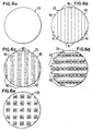
- the preferred manner of forming pins 22 is to machine them out of the top surface of plate 23 as illustrated in Figure 6.
- Figure 6(a) shows the top surface of metal plate 23.
- the next step is to fill grooves 41 with a rigid retainer material 42 such as a hard plastic, as illustrated in Figure 6(c).
- the purpose of retainers 42 is to prevent the breaking of the ridges 40 when generally perpendicular cuts are made to form a second set of generally parallel grooves 43 in said surface, as illustrated in Figure 6(d).
- the final step is to remove the remaining pieces of retainer material 42, thereby forming a set of protruding pins 22 as illustrated in Figure 6(e).
- FIG. 5 A preferred embodiment for making an electrostatic chuck 4 is illustrated in Figure 5.
- This chuck may or may not be a chuck 4 of the type depicted in Figs. 1-3.
- a chuck 4 of the Fig. 2-3 variety is shown.
- a lower dielectric element 30 and an upper dielectric element 33 are used.
- Lower dielectric 30 should be thicker than upper dielectric 33.
- Lower dielectric 30 needs to be relatively thick for purposes of mechanical support and to avoid the bowing of workpiece 2 in applications where heating is involved. (This latter reason also requires that metal plate 23 be relatively thick as well.)
- Upper dielectric 33 must be relatively thin because of the need to maximize the electrostatic forces pulling on workpiece 2.
- upper dielectric 33 is made to be too thin, it could crack, which would lead to undesirable arcing.
- a desirable thickness is between 5 mils and 10 mils. To achieve this thin of a layer, lapping rather than grinding is called for.
- Figure 5(b) illustrates a preferred embodiment, in which recesses 31,32 are ground or lapped out of the upper surface of lower dielectric 30. Holes 35,36 are drilled through dielectric 30 into recesses 31,32, respectively, to accommodate means for coupling electrodes 11,13 to voltage sources -V and +V.
- the recesses 31,32 are filled with brazing compound 11,13, as illustrated in Figure 5(c).
- This brazing compound can be the same as that described above to adhere pins 22 to dielectric 4.
- the holes 35,36 can either be filled with brazing compound or, as illustrated in Fig. 5(c), support the ends of wires 37,38 which are electrically connected to the patches 11,13 of brazing compound, respectively, and protrude downwardly from dielectric 30.
- the upper dielectric 33 is then placed onto the assembly of Figure 5(c) and the new assembly is heated above the melting point of the brazing compound. Upon cooling, surfaces 30 and 33 are brazed together, and electrodes 11,13 are automatically formed. The wires 37,38 are then connected to voltage sources -V and +V, respectively.
- the recess formation step of Figure 5(b) is optional, i.e., the brazing compound can be spread directly on the upper surface of dielectric 30 to form one or more patches. Forming the recesses 31,32, however, eliminates the air gap that would otherwise form between dielectrics 30,33. This air gap could contain undesirable impurities.
- the wires 37,38 can be formed to protrude from electrodes 11,13 outwardly rather than downwardly.
Landscapes
- Container, Conveyance, Adherence, Positioning, Of Wafer (AREA)
- Jigs For Machine Tools (AREA)
Applications Claiming Priority (3)
| Application Number | Priority Date | Filing Date | Title |
|---|---|---|---|
| US78922291A | 1991-11-07 | 1991-11-07 | |
| US789222 | 1991-11-07 | ||
| EP92310212A EP0541400B1 (fr) | 1991-11-07 | 1992-11-09 | Support électrostatique anti-adhésif pour un environnement à basse pression |
Related Parent Applications (2)
| Application Number | Title | Priority Date | Filing Date |
|---|---|---|---|
| EP92310212.3 Division | 1992-11-09 | ||
| EP92310212A Division EP0541400B1 (fr) | 1991-11-07 | 1992-11-09 | Support électrostatique anti-adhésif pour un environnement à basse pression |
Publications (3)
| Publication Number | Publication Date |
|---|---|
| EP0734055A2 true EP0734055A2 (fr) | 1996-09-25 |
| EP0734055A3 EP0734055A3 (fr) | 1996-11-27 |
| EP0734055B1 EP0734055B1 (fr) | 2000-07-26 |
Family
ID=25146963
Family Applications (2)
| Application Number | Title | Priority Date | Filing Date |
|---|---|---|---|
| EP96107414A Expired - Lifetime EP0734055B1 (fr) | 1991-11-07 | 1992-11-09 | Méthode de fabrication d'un support électrostatique |
| EP92310212A Expired - Lifetime EP0541400B1 (fr) | 1991-11-07 | 1992-11-09 | Support électrostatique anti-adhésif pour un environnement à basse pression |
Family Applications After (1)
| Application Number | Title | Priority Date | Filing Date |
|---|---|---|---|
| EP92310212A Expired - Lifetime EP0541400B1 (fr) | 1991-11-07 | 1992-11-09 | Support électrostatique anti-adhésif pour un environnement à basse pression |
Country Status (4)
| Country | Link |
|---|---|
| US (1) | US5426558A (fr) |
| EP (2) | EP0734055B1 (fr) |
| JP (1) | JP3332251B2 (fr) |
| DE (2) | DE69224791T2 (fr) |
Cited By (1)
| Publication number | Priority date | Publication date | Assignee | Title |
|---|---|---|---|---|
| KR20190134440A (ko) * | 2018-05-25 | 2019-12-04 | 블루 오션 리서치 & 네트워크 리미티드 | 세라믹제 정전 척의 제조 방법 |
Families Citing this family (40)
| Publication number | Priority date | Publication date | Assignee | Title |
|---|---|---|---|---|
| US5600530A (en) * | 1992-08-04 | 1997-02-04 | The Morgan Crucible Company Plc | Electrostatic chuck |
| US5631803A (en) * | 1995-01-06 | 1997-05-20 | Applied Materials, Inc. | Erosion resistant electrostatic chuck with improved cooling system |
| EP0669644B1 (fr) * | 1994-02-28 | 1997-08-20 | Applied Materials, Inc. | Support électrostatique |
| US5883778A (en) * | 1994-02-28 | 1999-03-16 | Applied Materials, Inc. | Electrostatic chuck with fluid flow regulator |
| US5535090A (en) * | 1994-03-03 | 1996-07-09 | Sherman; Arthur | Electrostatic chuck |
| JPH09213777A (ja) * | 1996-01-31 | 1997-08-15 | Kyocera Corp | 静電チャック |
| US5754391A (en) * | 1996-05-17 | 1998-05-19 | Saphikon Inc. | Electrostatic chuck |
| JP3455026B2 (ja) * | 1996-09-30 | 2003-10-06 | 京セラ株式会社 | 静電チャック |
| US6529362B2 (en) * | 1997-03-06 | 2003-03-04 | Applied Materials Inc. | Monocrystalline ceramic electrostatic chuck |
| US5833073A (en) * | 1997-06-02 | 1998-11-10 | Fluoroware, Inc. | Tacky film frame for electronic device |
| US5978202A (en) * | 1997-06-27 | 1999-11-02 | Applied Materials, Inc. | Electrostatic chuck having a thermal transfer regulator pad |
| JPH11157953A (ja) * | 1997-12-02 | 1999-06-15 | Nhk Spring Co Ltd | セラミックスと金属との構造体及びそれを用いた静電チャック装置 |
| JP3356115B2 (ja) * | 1999-05-20 | 2002-12-09 | ウシオ電機株式会社 | レジスト硬化装置 |
| US6248642B1 (en) | 1999-06-24 | 2001-06-19 | Ibis Technology Corporation | SIMOX using controlled water vapor for oxygen implants |
| US6423975B1 (en) | 1999-08-18 | 2002-07-23 | Ibis Technology, Inc. | Wafer holder for simox processing |
| US6155436A (en) * | 1999-08-18 | 2000-12-05 | Ibis Technology Corporation | Arc inhibiting wafer holder assembly |
| US6433342B1 (en) | 1999-08-18 | 2002-08-13 | Ibis Technology Corporation | Coated wafer holding pin |
| US6452195B1 (en) | 1999-08-18 | 2002-09-17 | Ibis Technology Corporation | Wafer holding pin |
| JP3492325B2 (ja) * | 2000-03-06 | 2004-02-03 | キヤノン株式会社 | 画像表示装置の製造方法 |
| JP3851489B2 (ja) * | 2000-04-27 | 2006-11-29 | 日本発条株式会社 | 静電チャック |
| TWI254403B (en) * | 2000-05-19 | 2006-05-01 | Ngk Insulators Ltd | Electrostatic clamper, and electrostatic attracting structures |
| US6583980B1 (en) * | 2000-08-18 | 2003-06-24 | Applied Materials Inc. | Substrate support tolerant to thermal expansion stresses |
| DE10330901B4 (de) * | 2002-07-08 | 2010-02-04 | Fraunhofer-Gesellschaft zur Förderung der angewandten Forschung e.V. | Elektrostatisches Fixierelement und Verfahren zu seiner Herstellung |
| US20070139855A1 (en) * | 2005-12-21 | 2007-06-21 | Asml Netherlands B.V. | Lithographic apparatus and method of manufacturing an electrostatic clamp for a lithographic apparatus |
| CN101221893B (zh) * | 2007-01-12 | 2010-05-19 | 北京北方微电子基地设备工艺研究中心有限责任公司 | 一种促进半导体晶片上静电电荷消散的方法 |
| US7667944B2 (en) * | 2007-06-29 | 2010-02-23 | Praxair Technology, Inc. | Polyceramic e-chuck |
| US20090075012A1 (en) * | 2007-09-13 | 2009-03-19 | Asml Netherlands B.V. | Lithographic apparatus and device manufacturing method |
| US9194189B2 (en) | 2011-09-19 | 2015-11-24 | Baker Hughes Incorporated | Methods of forming a cutting element for an earth-boring tool, a related cutting element, and an earth-boring tool including such a cutting element |
| US8684256B2 (en) * | 2011-11-30 | 2014-04-01 | Component Re-Engineering Company, Inc. | Method for hermetically joining plate and shaft devices including ceramic materials used in semiconductor processing |
| US9105492B2 (en) | 2012-05-08 | 2015-08-11 | LuxVue Technology Corporation | Compliant micro device transfer head |
| US9034754B2 (en) | 2012-05-25 | 2015-05-19 | LuxVue Technology Corporation | Method of forming a micro device transfer head with silicon electrode |
| US8569115B1 (en) | 2012-07-06 | 2013-10-29 | LuxVue Technology Corporation | Method of forming a compliant bipolar micro device transfer head with silicon electrodes |
| CN103578899B (zh) * | 2012-08-06 | 2016-08-24 | 中微半导体设备(上海)有限公司 | 等离子体处理设备及其静电卡盘 |
| US9255001B2 (en) | 2012-12-10 | 2016-02-09 | LuxVue Technology Corporation | Micro device transfer head array with metal electrodes |
| US9236815B2 (en) * | 2012-12-10 | 2016-01-12 | LuxVue Technology Corporation | Compliant micro device transfer head array with metal electrodes |
| EP3008553B1 (fr) | 2013-06-12 | 2023-06-07 | Rohinni, Inc. | Rétroéclairage de clavier au moyen de sources de génération de lumière réalisées par dépôt |
| US10629393B2 (en) | 2016-01-15 | 2020-04-21 | Rohinni, LLC | Apparatus and method of backlighting through a cover on the apparatus |
| JP6924618B2 (ja) | 2017-05-30 | 2021-08-25 | 東京エレクトロン株式会社 | 静電チャック及びプラズマ処理装置 |
| JP7059064B2 (ja) * | 2018-03-26 | 2022-04-25 | 株式会社日立ハイテク | プラズマ処理装置 |
| KR102472864B1 (ko) * | 2019-08-06 | 2022-12-02 | 주식회사 미코세라믹스 | 정전척 히터 및 그 제조방법 |
Family Cites Families (10)
| Publication number | Priority date | Publication date | Assignee | Title |
|---|---|---|---|---|
| JPS6059104B2 (ja) * | 1982-02-03 | 1985-12-23 | 株式会社東芝 | 静電チヤツク板 |
| JPS59124140A (ja) * | 1982-12-29 | 1984-07-18 | Fujitsu Ltd | 静電吸着装置 |
| JPS61192435A (ja) * | 1985-02-21 | 1986-08-27 | Canon Inc | 静電吸着保持装置 |
| US5103367A (en) * | 1987-05-06 | 1992-04-07 | Unisearch Limited | Electrostatic chuck using A.C. field excitation |
| JP2665242B2 (ja) * | 1988-09-19 | 1997-10-22 | 東陶機器株式会社 | 静電チャック |
| US5001594A (en) * | 1989-09-06 | 1991-03-19 | Mcnc | Electrostatic handling device |
| EP0439000B1 (fr) * | 1990-01-25 | 1994-09-14 | Applied Materials, Inc. | Dispositif de serrage électrostatique et procédé |
| FR2661039B1 (fr) * | 1990-04-12 | 1997-04-30 | Commissariat Energie Atomique | Porte-substrat electrostatique. |
| US5166856A (en) * | 1991-01-31 | 1992-11-24 | International Business Machines Corporation | Electrostatic chuck with diamond coating |
| US5155652A (en) * | 1991-05-02 | 1992-10-13 | International Business Machines Corporation | Temperature cycling ceramic electrostatic chuck |
-
1992
- 1992-11-09 EP EP96107414A patent/EP0734055B1/fr not_active Expired - Lifetime
- 1992-11-09 DE DE69224791T patent/DE69224791T2/de not_active Expired - Fee Related
- 1992-11-09 EP EP92310212A patent/EP0541400B1/fr not_active Expired - Lifetime
- 1992-11-09 JP JP32221892A patent/JP3332251B2/ja not_active Expired - Fee Related
- 1992-11-09 DE DE69231299T patent/DE69231299T2/de not_active Expired - Fee Related
-
1994
- 1994-03-14 US US08/213,459 patent/US5426558A/en not_active Expired - Fee Related
Cited By (2)
| Publication number | Priority date | Publication date | Assignee | Title |
|---|---|---|---|---|
| KR20190134440A (ko) * | 2018-05-25 | 2019-12-04 | 블루 오션 리서치 & 네트워크 리미티드 | 세라믹제 정전 척의 제조 방법 |
| KR102111291B1 (ko) | 2018-05-25 | 2020-05-19 | 블루 오션 리서치 & 네트워크 리미티드 | 세라믹제 정전 척의 제조 방법 |
Also Published As
| Publication number | Publication date |
|---|---|
| DE69231299T2 (de) | 2001-01-18 |
| DE69224791T2 (de) | 1998-07-09 |
| EP0734055B1 (fr) | 2000-07-26 |
| JPH05245734A (ja) | 1993-09-24 |
| US5426558A (en) | 1995-06-20 |
| EP0541400A3 (en) | 1993-06-30 |
| DE69231299D1 (de) | 2000-08-31 |
| JP3332251B2 (ja) | 2002-10-07 |
| DE69224791D1 (de) | 1998-04-23 |
| EP0541400A2 (fr) | 1993-05-12 |
| EP0541400B1 (fr) | 1998-03-18 |
| EP0734055A3 (fr) | 1996-11-27 |
Similar Documents
| Publication | Publication Date | Title |
|---|---|---|
| EP0541400B1 (fr) | Support électrostatique anti-adhésif pour un environnement à basse pression | |
| US5535090A (en) | Electrostatic chuck | |
| US5737178A (en) | Monocrystalline ceramic coating having integral bonding interconnects for electrostatic chucks | |
| US7416793B2 (en) | Electrostatic chuck and manufacturing method for the same, and alumina sintered member and manufacturing method for the same | |
| EP0628989B1 (fr) | Système de joint et méthode applicable pour les dispositifs de traitement de semi-conducteurs pour joindre des matériaux ayant des coefficients de dilatation thermique différents | |
| EP1070381B1 (fr) | Pince electrostatique pour plaquettes a faible contamination particulaire des plaquettes | |
| US6529362B2 (en) | Monocrystalline ceramic electrostatic chuck | |
| US5825607A (en) | Insulated wafer spacing mask for a substrate support chuck and method of fabricating same | |
| EP0049588B1 (fr) | Procédé et appareil pour le décapage à sec et dispositif de maintien électrostatique y utilisé | |
| US5280156A (en) | Wafer heating apparatus and with ceramic substrate and dielectric layer having electrostatic chucking means | |
| US6104596A (en) | Apparatus for retaining a subtrate in a semiconductor wafer processing system and a method of fabricating same | |
| US6141203A (en) | Electrostatic chuck | |
| EP0486966A1 (fr) | Appareil de maintien électrostatique | |
| US20050079737A1 (en) | Mems based contact conductivity electrostatic chuck | |
| WO1998057418A1 (fr) | Couche de couverture d'un mandrin porteur de substrats et son procede de fabrication | |
| EP1376660A2 (fr) | Dispositif de chauffage de plaquette semiconductrice contenant une fonction d'attraction électrostatique | |
| EP0680075B1 (fr) | Electrode pour la production de plasma et procede de fabrication de l'electrode | |
| JP3426845B2 (ja) | 静電チャック | |
| JPH09270454A (ja) | ウエハ保持装置 | |
| JPH11340309A (ja) | 導電体内蔵型セラミック製リフトピンとそれを用いた静電チャック | |
| JP2006080509A (ja) | 薄い基板支持体 | |
| WO2002001611A2 (fr) | Appareil permettant de supporter un substrat et procede de fabrication | |
| JP2007142456A (ja) | 静電チャック | |
| JP3965469B2 (ja) | 静電チャック | |
| Bang | Fabrication and Characterization of High Temperature Electrostatic Chucks |
Legal Events
| Date | Code | Title | Description |
|---|---|---|---|
| PUAI | Public reference made under article 153(3) epc to a published international application that has entered the european phase |
Free format text: ORIGINAL CODE: 0009012 |
|
| 17P | Request for examination filed |
Effective date: 19960521 |
|
| AC | Divisional application: reference to earlier application |
Ref document number: 541400 Country of ref document: EP |
|
| AK | Designated contracting states |
Kind code of ref document: A2 Designated state(s): DE FR GB |
|
| PUAL | Search report despatched |
Free format text: ORIGINAL CODE: 0009013 |
|
| AK | Designated contracting states |
Kind code of ref document: A3 Designated state(s): DE FR GB |
|
| 17Q | First examination report despatched |
Effective date: 19980326 |
|
| GRAG | Despatch of communication of intention to grant |
Free format text: ORIGINAL CODE: EPIDOS AGRA |
|
| GRAG | Despatch of communication of intention to grant |
Free format text: ORIGINAL CODE: EPIDOS AGRA |
|
| GRAH | Despatch of communication of intention to grant a patent |
Free format text: ORIGINAL CODE: EPIDOS IGRA |
|
| GRAH | Despatch of communication of intention to grant a patent |
Free format text: ORIGINAL CODE: EPIDOS IGRA |
|
| RAP1 | Party data changed (applicant data changed or rights of an application transferred) |
Owner name: VARIAN SEMICONDUCTOR EQUIPMENT ASSOCIATES INC. |
|
| GRAA | (expected) grant |
Free format text: ORIGINAL CODE: 0009210 |
|
| AC | Divisional application: reference to earlier application |
Ref document number: 541400 Country of ref document: EP |
|
| AK | Designated contracting states |
Kind code of ref document: B1 Designated state(s): DE FR GB |
|
| REF | Corresponds to: |
Ref document number: 69231299 Country of ref document: DE Date of ref document: 20000831 |
|
| ET | Fr: translation filed | ||
| PLBE | No opposition filed within time limit |
Free format text: ORIGINAL CODE: 0009261 |
|
| STAA | Information on the status of an ep patent application or granted ep patent |
Free format text: STATUS: NO OPPOSITION FILED WITHIN TIME LIMIT |
|
| 26N | No opposition filed | ||
| REG | Reference to a national code |
Ref country code: GB Ref legal event code: IF02 |
|
| PGFP | Annual fee paid to national office [announced via postgrant information from national office to epo] |
Ref country code: GB Payment date: 20031105 Year of fee payment: 12 |
|
| PGFP | Annual fee paid to national office [announced via postgrant information from national office to epo] |
Ref country code: FR Payment date: 20031119 Year of fee payment: 12 |
|
| PGFP | Annual fee paid to national office [announced via postgrant information from national office to epo] |
Ref country code: DE Payment date: 20031231 Year of fee payment: 12 |
|
| PG25 | Lapsed in a contracting state [announced via postgrant information from national office to epo] |
Ref country code: GB Free format text: LAPSE BECAUSE OF NON-PAYMENT OF DUE FEES Effective date: 20041109 |
|
| PG25 | Lapsed in a contracting state [announced via postgrant information from national office to epo] |
Ref country code: DE Free format text: LAPSE BECAUSE OF NON-PAYMENT OF DUE FEES Effective date: 20050601 |
|
| GBPC | Gb: european patent ceased through non-payment of renewal fee |
Effective date: 20041109 |
|
| PG25 | Lapsed in a contracting state [announced via postgrant information from national office to epo] |
Ref country code: FR Free format text: LAPSE BECAUSE OF NON-PAYMENT OF DUE FEES Effective date: 20050729 |
|
| REG | Reference to a national code |
Ref country code: FR Ref legal event code: ST |