EP0735397A2 - Dispositif micro-optique pour transformer des faisceaux d'un arrangement de diodes laser et procédé de fabrication d'un tel dispositif - Google Patents
Dispositif micro-optique pour transformer des faisceaux d'un arrangement de diodes laser et procédé de fabrication d'un tel dispositif Download PDFInfo
- Publication number
- EP0735397A2 EP0735397A2 EP96103557A EP96103557A EP0735397A2 EP 0735397 A2 EP0735397 A2 EP 0735397A2 EP 96103557 A EP96103557 A EP 96103557A EP 96103557 A EP96103557 A EP 96103557A EP 0735397 A2 EP0735397 A2 EP 0735397A2
- Authority
- EP
- European Patent Office
- Prior art keywords
- micro
- optical device
- laser beams
- individual
- mirrors
- Prior art date
- Legal status (The legal status is an assumption and is not a legal conclusion. Google has not performed a legal analysis and makes no representation as to the accuracy of the status listed.)
- Granted
Links
- 238000000034 method Methods 0.000 title claims abstract description 15
- 238000004519 manufacturing process Methods 0.000 title claims description 5
- 230000001131 transforming effect Effects 0.000 title 1
- 239000004065 semiconductor Substances 0.000 claims abstract description 17
- 239000000463 material Substances 0.000 claims abstract description 15
- 238000005516 engineering process Methods 0.000 claims abstract description 5
- 238000005530 etching Methods 0.000 claims description 4
- 230000003287 optical effect Effects 0.000 claims description 4
- 239000011521 glass Substances 0.000 description 6
- 238000007493 shaping process Methods 0.000 description 5
- 230000008878 coupling Effects 0.000 description 4
- 238000010168 coupling process Methods 0.000 description 4
- 238000005859 coupling reaction Methods 0.000 description 4
- 239000004033 plastic Substances 0.000 description 4
- 229920003023 plastic Polymers 0.000 description 4
- 229910001218 Gallium arsenide Inorganic materials 0.000 description 3
- 229910004298 SiO 2 Inorganic materials 0.000 description 3
- 229910052782 aluminium Inorganic materials 0.000 description 3
- XAGFODPZIPBFFR-UHFFFAOYSA-N aluminium Chemical compound [Al] XAGFODPZIPBFFR-UHFFFAOYSA-N 0.000 description 3
- 229910052751 metal Inorganic materials 0.000 description 3
- 239000002184 metal Substances 0.000 description 3
- 238000004026 adhesive bonding Methods 0.000 description 2
- 238000000576 coating method Methods 0.000 description 2
- 238000005476 soldering Methods 0.000 description 2
- 238000004544 sputter deposition Methods 0.000 description 2
- 229910000881 Cu alloy Inorganic materials 0.000 description 1
- 229910005540 GaP Inorganic materials 0.000 description 1
- 229910001182 Mo alloy Inorganic materials 0.000 description 1
- 238000004364 calculation method Methods 0.000 description 1
- 238000005266 casting Methods 0.000 description 1
- 239000011248 coating agent Substances 0.000 description 1
- 239000004020 conductor Substances 0.000 description 1
- 238000007516 diamond turning Methods 0.000 description 1
- 230000008020 evaporation Effects 0.000 description 1
- 238000001704 evaporation Methods 0.000 description 1
- 238000002347 injection Methods 0.000 description 1
- 239000007924 injection Substances 0.000 description 1
- 238000010297 mechanical methods and process Methods 0.000 description 1
- 230000005226 mechanical processes and functions Effects 0.000 description 1
- 229910003465 moissanite Inorganic materials 0.000 description 1
- 238000003825 pressing Methods 0.000 description 1
- 230000005855 radiation Effects 0.000 description 1
- 229910010271 silicon carbide Inorganic materials 0.000 description 1
- 238000007740 vapor deposition Methods 0.000 description 1
Images


Classifications
-
- G—PHYSICS
- G02—OPTICS
- G02B—OPTICAL ELEMENTS, SYSTEMS OR APPARATUS
- G02B19/00—Condensers, e.g. light collectors or similar non-imaging optics
- G02B19/0033—Condensers, e.g. light collectors or similar non-imaging optics characterised by the use
- G02B19/0047—Condensers, e.g. light collectors or similar non-imaging optics characterised by the use for use with a light source
- G02B19/0052—Condensers, e.g. light collectors or similar non-imaging optics characterised by the use for use with a light source the light source comprising a laser diode
- G02B19/0057—Condensers, e.g. light collectors or similar non-imaging optics characterised by the use for use with a light source the light source comprising a laser diode in the form of a laser diode array, e.g. laser diode bar
-
- G—PHYSICS
- G02—OPTICS
- G02B—OPTICAL ELEMENTS, SYSTEMS OR APPARATUS
- G02B19/00—Condensers, e.g. light collectors or similar non-imaging optics
- G02B19/0004—Condensers, e.g. light collectors or similar non-imaging optics characterised by the optical means employed
- G02B19/0028—Condensers, e.g. light collectors or similar non-imaging optics characterised by the optical means employed refractive and reflective surfaces, e.g. non-imaging catadioptric systems
-
- G—PHYSICS
- G02—OPTICS
- G02B—OPTICAL ELEMENTS, SYSTEMS OR APPARATUS
- G02B27/00—Optical systems or apparatus not provided for by any of the groups G02B1/00 - G02B26/00, G02B30/00
- G02B27/10—Beam splitting or combining systems
- G02B27/1086—Beam splitting or combining systems operating by diffraction only
-
- G—PHYSICS
- G02—OPTICS
- G02B—OPTICAL ELEMENTS, SYSTEMS OR APPARATUS
- G02B27/00—Optical systems or apparatus not provided for by any of the groups G02B1/00 - G02B26/00, G02B30/00
- G02B27/10—Beam splitting or combining systems
- G02B27/12—Beam splitting or combining systems operating by refraction only
- G02B27/123—The splitting element being a lens or a system of lenses, including arrays and surfaces with refractive power
-
- H—ELECTRICITY
- H01—ELECTRIC ELEMENTS
- H01S—DEVICES USING THE PROCESS OF LIGHT AMPLIFICATION BY STIMULATED EMISSION OF RADIATION [LASER] TO AMPLIFY OR GENERATE LIGHT; DEVICES USING STIMULATED EMISSION OF ELECTROMAGNETIC RADIATION IN WAVE RANGES OTHER THAN OPTICAL
- H01S5/00—Semiconductor lasers
- H01S5/40—Arrangement of two or more semiconductor lasers, not provided for in groups H01S5/02 - H01S5/30
- H01S5/4025—Array arrangements, e.g. constituted by discrete laser diodes or laser bar
-
- H—ELECTRICITY
- H01—ELECTRIC ELEMENTS
- H01S—DEVICES USING THE PROCESS OF LIGHT AMPLIFICATION BY STIMULATED EMISSION OF RADIATION [LASER] TO AMPLIFY OR GENERATE LIGHT; DEVICES USING STIMULATED EMISSION OF ELECTROMAGNETIC RADIATION IN WAVE RANGES OTHER THAN OPTICAL
- H01S3/00—Lasers, i.e. devices using stimulated emission of electromagnetic radiation in the infrared, visible or ultraviolet wave range
- H01S3/005—Optical devices external to the laser cavity, specially adapted for lasers, e.g. for homogenisation of the beam or for manipulating laser pulses, e.g. pulse shaping
-
- H—ELECTRICITY
- H01—ELECTRIC ELEMENTS
- H01S—DEVICES USING THE PROCESS OF LIGHT AMPLIFICATION BY STIMULATED EMISSION OF RADIATION [LASER] TO AMPLIFY OR GENERATE LIGHT; DEVICES USING STIMULATED EMISSION OF ELECTROMAGNETIC RADIATION IN WAVE RANGES OTHER THAN OPTICAL
- H01S5/00—Semiconductor lasers
- H01S5/005—Optical components external to the laser cavity, specially adapted therefor, e.g. for homogenisation or merging of the beams or for manipulating laser pulses, e.g. pulse shaping
Definitions
- the invention relates to a micro-optical device for converting a first laser beam emitted by one or more laser diode bars or a number of individual laser diodes in the x-direction of an orthogonal reference system, consisting of a plurality of individual laser beams with a strip-shaped cross section, into a second laser beam.
- Such a micro-optical device is known, for example, from J.R. Hobbs, "Diode pumped solid-state lasers: Offset-plane mirrors transform laserbeam", Laser Focus World, May 1994, p.47.
- the micro-optical device described therein consists of two highly reflecting mirrors arranged parallel to one another at a distance. The two mirrors are offset vertically and horizontally.
- the first laser beam bundle of a laser diode bar that is incident at an angle ⁇ , with 0 ° ⁇ ⁇ 190 °, to the mirror surface normal is converted into the second laser beam bundle from strip-shaped individual laser beams arranged parallel to one another by means of suitable multiple total reflection between the two mirrors.
- a major difficulty of this mirror system is that a highly precise adjustment of the two mirrors to one another and the pair of mirrors to the incident first laser beam is necessary for effective beam shaping.
- the reflection losses are very high due to the multiple reflection within the pair of mirrors.
- the maximum forming efficiency achieved is around 70%.
- the invention is therefore based on the object of developing a micro-optical device of the type mentioned at the outset, which is easy to adjust and its forming efficiency is between 90% and 100%.
- a micro-optical device should be inexpensive to manufacture.
- a beam paralleling optical system parallelizes the individual laser beams of the first laser beam which are divergent in the z-direction of the reference system, and in that a deflecting mirror arrangement then transforms the laser beam consisting of the parallelized strip-shaped individual laser beams into the second laser beam.
- This micro-optical device can consist, for example, of a semiconductor material which is transparent to the wavelength of the laser light emitted by the laser diode field.
- the laser beam can then be guided in the semiconductor material, whereby the beam expansion of the individual laser beams and thus the radiation loss can be reduced.
- the structures of the beam parallelization optics and the deflecting mirror arrangement can be produced by means of known etching techniques of semiconductor process technology. This ensures cost-effective production of the micro-optical device.
- the exemplary embodiments described below each serve to deform a laser beam 8, which is emitted by a laser diode bar 6 according to FIG. 2.
- the laser diode bar 6 consists of seven individual laser diodes 7.
- the pn junctions of the individual laser diodes 7 lie parallel to the xy plane of an orthogonal reference system 5.
- Each individual laser diode 7 emits an individual laser beam 9 of the width ⁇ y, which is only one parallel to the pn junction of the individual laser diode very weak and strong divergence perpendicular to the pn junction.
- laser diode bar 6 instead of the laser diode bar 6, a plurality of laser diode bars or a number of individual laser diode chips can of course also be used in all the exemplary embodiments.
- the first exemplary embodiment of a micro-optical device according to the invention is constructed on a base plate 1.
- the base plate 1 consists, for example, of a Mo / Cu alloy or another good heat-conducting material, the coefficient of thermal expansion of which is the coefficient of thermal expansion of the others Components of the micro-optical device is adapted.
- the top of the base plate 1 is divided by a vertical step 2 into two surfaces 3, 4, which are parallel to the xy plane of the orthogonal reference system 5.
- the laser diode bar 6 is attached to the higher surface 3, for example by means of soldering or gluing, in such a way that the laser light exit surface 10 of the laser diode bar 6 is flush with the vertical surface of stage 2.
- the individual laser beams 9 are thus emitted in the x direction.
- a plano-convex cylindrical lens 11 is attached to the lower surface 4 and adjoins the laser light exit surface 10 with its curved surface. However, it can also be arranged at a small distance from the light exit surface 10, such that the curved surface and the light exit surface 10 face each other.
- the cylindrical lens 11 is produced, for example, from glass, plastic or from a semiconductor material which is transparent to the wavelength of the laser light of the individual laser diodes. Semiconductor materials are particularly suitable for this application due to their large refractive index. For example, SiC can be used for light wavelengths ⁇ > 400 nm, GaP for ⁇ > 500 nm, GaAs for ⁇ > 900 nm and Si for ⁇ > 1100 nm.
- the cylindrical lens 11 parallelizes the individual laser beams 9, which are very divergent in the z-direction of the reference system 5.
- the longitudinal cross-sectional central axes of the individual laser beams 12 lie on a single straight line parallel to the y-axis of the reference system 5.
- the parallelized individual laser beams 12 are shown by their beam axes.
- a diffractive optic or a combination of a cylindrical lens and a diffractive optic can also be used.
- a row of mirrors 14 consisting of seven individual mirrors 13 is fastened on the surface 4 in the beam propagation direction (+ x direction) after the cylindrical lens 11. It is made of metal or a semiconductor material, for example, and the mirror surfaces are coated and / or polished with a reflection-enhancing material such as aluminum or SiO 2 / Si, for example by means of vapor deposition or sputtering.
- the mirror surface normals of the individual mirrors 13 form an angle of 45 ° with the beam axes of the parallelized individual laser beams 12 and run parallel to the xz plane of the reference system 5.
- Each individual mirror 13 is displaced parallel to its neighboring individual mirrors 13 in the x direction by ⁇ z + ⁇ , so that the row of mirrors 14 has a step-like structure.
- ⁇ z is the beam height in the z direction and ⁇ is the distance between the strip-shaped individual laser beams 12 shown in FIG. 4 after the laser beam 31 has been transformed into the laser beam 17 when the individual laser beams 12 are exactly orthogonal.
- the width and length of the mirror surfaces of the individual mirrors 13 is ⁇ y + ⁇ or at least ⁇ z / cos45 ° .
- ⁇ y is the width of an individual laser beam 9 after emerging from the laser diode bar 6 and ⁇ is the distance between two individual laser beams 9.
- the parallelized individual laser beams 12 are deflected by 90 ° in the z direction and at the same time offset in the x direction, such that no two individual laser beams 12 lie with their cross-sectional longitudinal center axis on a common straight line.
- Another row of mirrors 15 with seven individual mirrors 16 is arranged above the row of mirrors 14.
- the row of mirrors 15 is produced, for example, in exactly the same way as the row of mirrors 14.
- the mirror surface normals of the individual mirrors 16 form an angle of 45 ° with the beam axes of the individual laser beams 12 deflected by 90 ° in the z direction and run parallel to the yz plane of the reference system 5.
- Each individual mirror 16 is shifted parallel to its neighboring individual mirrors 16 in the y direction by ⁇ y + ⁇ , so that the row of mirrors 15 has a step-like structure.
- the width and length of the mirror surfaces of the individual mirrors 16 are ⁇ z + ⁇ and ( ⁇ y + ⁇ ) / cos45 ° .
- the individual mirrors 13, 16 are arranged relative to one another in such a way that the center points of the mirror surfaces of two individual mirrors 13, 16 lie exactly one above the other in the z direction.
- the row of mirrors 15 deflects the individual laser beams 12 deflected by the row of mirrors 14 in the z direction by 90 ° in the y direction and images the individual laser beams 12 in parallel next to one another according to FIG.
- the deflecting mirror arrangement shown schematically in FIG. 3 of the second exemplary embodiment of the micro-optical device according to the invention likewise consists of two rows of mirrors 18, 21 each consisting of seven individual mirrors 19, 20.
- the arrangement and size of the individual mirrors 19, 20 and the arrangement of the remaining components of the micro-optical device are identical
- the first embodiment The difference from the rows of mirrors 14, 15 is that the individual laser beams 12 are guided after the cylindrical lens 11 not in air but in a medium which is transparent to the wavelength of the laser light emitted by the individual laser diodes.
- the interfaces between the translucent medium and air or another adjacent medium thus form the mirror surfaces of the individual mirrors 19, 20.
- the individual mirrors 19, 20 are formed, for example, by recesses from a single cuboid consisting of the permeable medium.
- SiC can also be used as the medium, for example for a light wavelength ⁇ > 400 nm, for ⁇ > 550 nm GaP, for ⁇ > 900 nm GaAs and for ⁇ > 1100 nm Si.
- the advantage of these semiconductor materials is that, owing to their high refractive index, no coating of the mirror surfaces of the individual mirrors 19, 20 is required.
- the mirror surfaces can be improved with aluminum or with another suitable material to improve the reflective properties be coated. Evaporation, sputtering, CVD or another method known from semiconductor process technology can be used as the coating method.
- the parallel individual beams 12 enter the row of mirrors 18 through a light entry surface 22 and are deflected by 90 ° in the z direction on the individual mirrors 19 and at the same time offset in the x direction. Subsequently, the individual laser beams 12 are deflected by the individual mirrors 20 by 90 ° in the y direction and emerge from the row of mirrors 21 through a light exit surface 23.
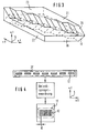
- FIG. 4 schematically shows the shaping of the laser beam 31 by means of the deflecting mirror arrangement according to exemplary embodiment one or two.
- the laser beam bundle 31 consisting of seven parallelized individual laser beams 12 is converted into a rectangular laser beam bundle 17 consisting of seven parallelized individual laser beams 12 arranged next to one another at a distance ⁇ .
- a simplification of the two exemplary embodiments one and two described above can be achieved in that the row of mirrors 14 and 18 is replaced by a single larger mirror.
- This mirror must be mounted in such a way that its mirror surface normal includes an angle of 45 ° with the xy plane of the reference system 5 and an angle ⁇ > 0 ° with the xz plane.
- the width of the oblique mirror is (Length of the laser diode bar 6) * cos ⁇ and the height of the oblique mirror is at least ⁇ z / cos45 ° .
- the row of mirrors 15 and 21 remains unchanged in terms of structure.
- the width of the individual mirrors 16 and 20 is, however ( ⁇ y + ⁇ ) * tan ⁇ .
- the third exemplary embodiment of the micro-optical device according to the invention has a single mirror row 24 instead of two rows of mirrors, each of which performs a 90 ° deflection.
- This row of mirrors shown in Figure 5 24 consists of seven individual mirrors 25, the mirror surface normals of which have an angle of 45 ° with the xz plane of the reference system 5 and an angle ⁇ > 0 ° with the xy plane.
- the centers of the mirror surfaces of the individual mirrors 25 lie on a single straight line running parallel to the y-axis of the reference system 5 and are at a distance of ⁇ y + ⁇ from one another.
- the length of the individual mirror 25 is at least ⁇ y / cos45 ° and the width at least ⁇ z / cos ⁇ .
- the angle ⁇ is selected such that each parallelized individual laser beam 12 is guided over the individual mirror 25 following in the + y direction after reflection at the associated individual mirror 25.
- the width of the individual mirrors 25 and the angle ⁇ should be as small as possible.
- the minimum size of the angle ⁇ depends on the distance between the individual laser diodes and on the width of the individual mirrors 25.
- the fourth exemplary embodiment of a micro-optical device according to the invention is in principle identical to the third exemplary embodiment.
- the difference is that the row of mirrors 26 with the individual mirrors 27 is designed in such a way that the individual laser beams 12 are guided not in air but in a light-conducting medium.
- the medium is transparent to the wavelength of the laser light emitted by the individual laser diodes.
- the row of mirrors 26 can be made, for example, from the materials already mentioned in the second exemplary embodiment.
- the individual mirrors 27 are formed, for example, by wedge-shaped recesses from a cuboid, consisting of the medium which is permeable to the laser light of the individual laser diodes.
- the mirror surfaces are coated and / or polished, for example with aluminum or SiO 2 / Si (possibly alternating layers, ie alternately SiO 2 and Si).
- the row of mirrors 26 is by means of a coupling plate 28, which likewise consists of a material which is transparent to the wavelength of the laser light, coupled to the cylindrical lens 11.
- the row of mirrors 26 and the coupling plate 28 can also consist of a single part.
- a plate can be arranged between the row of mirrors 26 and the laser diode bar, in which the cylindrical lens 11 and / or further lenses are introduced or formed.
- This plate can consist of a semiconductor material.
- the lens (s) can be manufactured using conventional semiconductor processes.
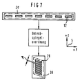
- FIG. 7 schematically shows the shaping of the laser beam 31 by means of the deflecting mirror arrangement according to exemplary embodiment three or four.
- the laser beam bundle 31 consisting of seven parallelized strip-shaped individual laser beams 12 is converted into a parallelogram-shaped laser beam bundle 30 consisting of seven parallelized strip-shaped individual laser beams 29 arranged next to one another in parallel at a distance ⁇ .
- the individual laser beams 9 for the pn junction of the individual laser beams are not exactly parallel, as assumed above, but rather weakly divergent.
- the mirror dimensions must therefore be adjusted accordingly.
- the minimum dimensions given above change towards larger values.
- the individual laser beams 12 are not exactly parallelized but rather weakly divergent.
- the values of ⁇ y and ⁇ z on the mirror surfaces of those mirrors which are furthest away from the light exit surface 10 in the beam direction are always decisive for the calculation.
- the guidance of the individual laser beams 9, 12, 29 in an optical medium has the advantage that their expansion can be avoided.
- the light exit surface 10 of the cylindrical lens 11 can advantageously directly adjoin the light entry surface 22 or 32 of the mirror row 18 or the coupling plate 28. Thereby the number of optical interfaces that cause reflection losses can be minimized in the micro-optical device. It is also conceivable that the mirror rows or rows and the cylindrical lens are made from one part.
- the mirror arrangements described above and the cylindrical lens are characterized in an advantageous manner in that they can be produced using inexpensive processes.
- Plano-convex cylindrical lenses made of semiconductor materials can be produced, for example, on a wafer using known etching processes. The wafer is then cut into individual lenses of suitable length and width.
- the rows of mirrors can be produced, for example, using Si, GaP, GaAs, SiC, metal or glass using etching processes known in semiconductor process technology. However, injection, pressing and casting processes for plastic, glass or metal can also be used in the same way. For the production of the forms, for. B. the so-called LIGA method can be used.
- the mirror structures can also be produced using mechanical processes such as the micro-precision diamond turning process. It is also possible to line up structured glass panes by anodic bonding, soldering or gluing. In the case of plastics, the mirror structure can be produced by mechanical processing or as a molded part.
- the deflecting mirror arrangements described in the exemplary embodiments are designed exclusively for seven individual laser beams, the micro-optical device according to the invention can be used for any number of individual laser beams. It is only necessary to adjust the number of individual mirrors.
Landscapes
- Physics & Mathematics (AREA)
- General Physics & Mathematics (AREA)
- Optics & Photonics (AREA)
- Condensed Matter Physics & Semiconductors (AREA)
- Electromagnetism (AREA)
- Semiconductor Lasers (AREA)
- Laser Beam Processing (AREA)
- Lasers (AREA)
- Optical Elements Other Than Lenses (AREA)
Applications Claiming Priority (2)
| Application Number | Priority Date | Filing Date | Title |
|---|---|---|---|
| DE19511593A DE19511593C2 (de) | 1995-03-29 | 1995-03-29 | Mikrooptische Vorrichtung |
| DE19511593 | 1995-03-29 |
Publications (3)
| Publication Number | Publication Date |
|---|---|
| EP0735397A2 true EP0735397A2 (fr) | 1996-10-02 |
| EP0735397A3 EP0735397A3 (fr) | 1997-04-02 |
| EP0735397B1 EP0735397B1 (fr) | 2002-06-12 |
Family
ID=7758100
Family Applications (1)
| Application Number | Title | Priority Date | Filing Date |
|---|---|---|---|
| EP96103557A Revoked EP0735397B1 (fr) | 1995-03-29 | 1996-03-06 | Dispositif micro-optique pour transformer des faisceaux d'un arrangement de diodes laser et procédé de fabrication d'un tel dispositif |
Country Status (9)
| Country | Link |
|---|---|
| US (1) | US5808323A (fr) |
| EP (1) | EP0735397B1 (fr) |
| JP (1) | JP2991968B2 (fr) |
| KR (1) | KR960035074A (fr) |
| CN (1) | CN1080417C (fr) |
| CA (1) | CA2173059C (fr) |
| DE (2) | DE19511593C2 (fr) |
| IN (1) | IN187666B (fr) |
| TW (1) | TW317034B (fr) |
Cited By (3)
| Publication number | Priority date | Publication date | Assignee | Title |
|---|---|---|---|---|
| EP0903823A3 (fr) * | 1997-09-22 | 2000-07-12 | Siemens Aktiengesellschaft | Elément laser comprenant un réseau à laser et méthode de fabrication |
| WO2010084001A1 (fr) * | 2009-01-23 | 2010-07-29 | Limo Patentverwaltung Gmbh & Co. Kg | Dispositif de mise en forme d'un faisceau de réseaux de diodes laser |
| CN102096291A (zh) * | 2009-12-09 | 2011-06-15 | 精工爱普生株式会社 | 发光装置以及投影仪 |
Families Citing this family (82)
| Publication number | Priority date | Publication date | Assignee | Title |
|---|---|---|---|---|
| DE19780124B4 (de) * | 1996-02-23 | 2007-02-15 | Fraunhofer-Gesellschaft zur Förderung der angewandten Forschung e.V. | Anordnung zur Formung des geometrischen Querschnitts mehrerer Festkörper- und/oder Halbleiterlaser |
| DE19706276B4 (de) * | 1997-02-18 | 2011-01-13 | Siemens Ag | Halbleiterlaser-Vorrichtung und Verfahren zum Herstellen einer Halbleiterlaser-Vorrichtung |
| DE19706279A1 (de) * | 1997-02-18 | 1998-08-20 | Siemens Ag | Laservorrichtung |
| AU747260B2 (en) | 1997-07-25 | 2002-05-09 | Nichia Chemical Industries, Ltd. | Nitride semiconductor device |
| DE59813644D1 (de) * | 1997-09-05 | 2006-08-31 | Osram Opto Semiconductors Gmbh | Immersionssystem |
| US6872984B1 (en) | 1998-07-29 | 2005-03-29 | Silicon Light Machines Corporation | Method of sealing a hermetic lid to a semiconductor die at an angle |
| US6303986B1 (en) | 1998-07-29 | 2001-10-16 | Silicon Light Machines | Method of and apparatus for sealing an hermetic lid to a semiconductor die |
| JP3770014B2 (ja) | 1999-02-09 | 2006-04-26 | 日亜化学工業株式会社 | 窒化物半導体素子 |
| ATE452445T1 (de) | 1999-03-04 | 2010-01-15 | Nichia Corp | Nitridhalbleiterlaserelement |
| US6356577B1 (en) * | 1999-07-15 | 2002-03-12 | Silicon Light Machines | Method and apparatus for combining light output from multiple laser diode bars |
| JP4748836B2 (ja) * | 1999-08-13 | 2011-08-17 | 株式会社半導体エネルギー研究所 | レーザ照射装置 |
| US6504650B1 (en) | 1999-10-19 | 2003-01-07 | Anthony J. Alfrey | Optical transformer and system using same |
| US6407870B1 (en) | 1999-10-28 | 2002-06-18 | Ihar Hurevich | Optical beam shaper and method for spatial redistribution of inhomogeneous beam |
| JP2001215443A (ja) * | 2000-02-04 | 2001-08-10 | Hamamatsu Photonics Kk | 光学装置 |
| US6956878B1 (en) | 2000-02-07 | 2005-10-18 | Silicon Light Machines Corporation | Method and apparatus for reducing laser speckle using polarization averaging |
| EP1215523A3 (fr) * | 2000-12-16 | 2004-05-26 | Hentze-Lissotschenko Patentverwaltungs GmbH & Co.KG | Système d'irradiation avec transformation du faisceau pour générer une radiation modulée |
| US7177081B2 (en) | 2001-03-08 | 2007-02-13 | Silicon Light Machines Corporation | High contrast grating light valve type device |
| DE10113019A1 (de) * | 2001-03-17 | 2002-09-19 | Lissotschenko Vitalij | Strahlformungsvorrichtung, Anordnung zur Einkopplung eines Lichtstrahls in eine Lichtleitfaser sowie Strahldreheinheit für eine derartige Strahlformungsvorrichtung oder eine derartige Anordnung |
| CN1313861C (zh) * | 2001-03-30 | 2007-05-02 | 新日本制铁株式会社 | 半导体激光装置和采用它的固体激光装置 |
| US6707591B2 (en) | 2001-04-10 | 2004-03-16 | Silicon Light Machines | Angled illumination for a single order light modulator based projection system |
| US6865346B1 (en) | 2001-06-05 | 2005-03-08 | Silicon Light Machines Corporation | Fiber optic transceiver |
| US6747781B2 (en) | 2001-06-25 | 2004-06-08 | Silicon Light Machines, Inc. | Method, apparatus, and diffuser for reducing laser speckle |
| US6782205B2 (en) | 2001-06-25 | 2004-08-24 | Silicon Light Machines | Method and apparatus for dynamic equalization in wavelength division multiplexing |
| US6829092B2 (en) | 2001-08-15 | 2004-12-07 | Silicon Light Machines, Inc. | Blazed grating light valve |
| US6930364B2 (en) | 2001-09-13 | 2005-08-16 | Silicon Light Machines Corporation | Microelectronic mechanical system and methods |
| US6956995B1 (en) | 2001-11-09 | 2005-10-18 | Silicon Light Machines Corporation | Optical communication arrangement |
| US6800238B1 (en) | 2002-01-15 | 2004-10-05 | Silicon Light Machines, Inc. | Method for domain patterning in low coercive field ferroelectrics |
| FI116010B (fi) * | 2002-05-22 | 2005-08-31 | Cavitar Oy | Menetelmä ja laserlaite suuren optisen tehotiheyden tuottamiseksi |
| US6728023B1 (en) | 2002-05-28 | 2004-04-27 | Silicon Light Machines | Optical device arrays with optimized image resolution |
| US6767751B2 (en) | 2002-05-28 | 2004-07-27 | Silicon Light Machines, Inc. | Integrated driver process flow |
| US7054515B1 (en) | 2002-05-30 | 2006-05-30 | Silicon Light Machines Corporation | Diffractive light modulator-based dynamic equalizer with integrated spectral monitor |
| US6822797B1 (en) | 2002-05-31 | 2004-11-23 | Silicon Light Machines, Inc. | Light modulator structure for producing high-contrast operation using zero-order light |
| US6829258B1 (en) | 2002-06-26 | 2004-12-07 | Silicon Light Machines, Inc. | Rapidly tunable external cavity laser |
| US6714337B1 (en) | 2002-06-28 | 2004-03-30 | Silicon Light Machines | Method and device for modulating a light beam and having an improved gamma response |
| US6908201B2 (en) | 2002-06-28 | 2005-06-21 | Silicon Light Machines Corporation | Micro-support structures |
| US6813059B2 (en) | 2002-06-28 | 2004-11-02 | Silicon Light Machines, Inc. | Reduced formation of asperities in contact micro-structures |
| US6801354B1 (en) | 2002-08-20 | 2004-10-05 | Silicon Light Machines, Inc. | 2-D diffraction grating for substantially eliminating polarization dependent losses |
| US7057795B2 (en) | 2002-08-20 | 2006-06-06 | Silicon Light Machines Corporation | Micro-structures with individually addressable ribbon pairs |
| CN2566292Y (zh) * | 2002-09-03 | 2003-08-13 | 钱定榕 | 光束分配装置 |
| US6712480B1 (en) | 2002-09-27 | 2004-03-30 | Silicon Light Machines | Controlled curvature of stressed micro-structures |
| US6928207B1 (en) | 2002-12-12 | 2005-08-09 | Silicon Light Machines Corporation | Apparatus for selectively blocking WDM channels |
| US7057819B1 (en) | 2002-12-17 | 2006-06-06 | Silicon Light Machines Corporation | High contrast tilting ribbon blazed grating |
| US6987600B1 (en) | 2002-12-17 | 2006-01-17 | Silicon Light Machines Corporation | Arbitrary phase profile for better equalization in dynamic gain equalizer |
| US6934070B1 (en) | 2002-12-18 | 2005-08-23 | Silicon Light Machines Corporation | Chirped optical MEM device |
| US6927891B1 (en) | 2002-12-23 | 2005-08-09 | Silicon Light Machines Corporation | Tilt-able grating plane for improved crosstalk in 1×N blaze switches |
| US7068372B1 (en) | 2003-01-28 | 2006-06-27 | Silicon Light Machines Corporation | MEMS interferometer-based reconfigurable optical add-and-drop multiplexor |
| JP4153438B2 (ja) | 2003-01-30 | 2008-09-24 | 富士フイルム株式会社 | レーザ光合波方法および装置 |
| US7286764B1 (en) | 2003-02-03 | 2007-10-23 | Silicon Light Machines Corporation | Reconfigurable modulator-based optical add-and-drop multiplexer |
| US6947613B1 (en) | 2003-02-11 | 2005-09-20 | Silicon Light Machines Corporation | Wavelength selective switch and equalizer |
| US6922272B1 (en) | 2003-02-14 | 2005-07-26 | Silicon Light Machines Corporation | Method and apparatus for leveling thermal stress variations in multi-layer MEMS devices |
| US7391973B1 (en) | 2003-02-28 | 2008-06-24 | Silicon Light Machines Corporation | Two-stage gain equalizer |
| US6806997B1 (en) | 2003-02-28 | 2004-10-19 | Silicon Light Machines, Inc. | Patterned diffractive light modulator ribbon for PDL reduction |
| US6829077B1 (en) | 2003-02-28 | 2004-12-07 | Silicon Light Machines, Inc. | Diffractive light modulator with dynamically rotatable diffraction plane |
| US7027202B1 (en) | 2003-02-28 | 2006-04-11 | Silicon Light Machines Corp | Silicon substrate as a light modulator sacrificial layer |
| US6922273B1 (en) | 2003-02-28 | 2005-07-26 | Silicon Light Machines Corporation | PDL mitigation structure for diffractive MEMS and gratings |
| US7042611B1 (en) | 2003-03-03 | 2006-05-09 | Silicon Light Machines Corporation | Pre-deflected bias ribbons |
| US6870682B1 (en) | 2003-09-30 | 2005-03-22 | Institut National D'optique | Apparatus for reshaping an optical beam bundle |
| US20060280209A1 (en) * | 2005-02-11 | 2006-12-14 | Hans-Georg Treusch | Beam combining methods and devices with high output intensity |
| US20070268572A1 (en) * | 2006-05-20 | 2007-11-22 | Newport Corporation | Multiple emitter coupling devices and methods with beam transform system |
| US7830608B2 (en) * | 2006-05-20 | 2010-11-09 | Oclaro Photonics, Inc. | Multiple emitter coupling devices and methods with beam transform system |
| US7680170B2 (en) * | 2006-06-15 | 2010-03-16 | Oclaro Photonics, Inc. | Coupling devices and methods for stacked laser emitter arrays |
| US20070291373A1 (en) * | 2006-06-15 | 2007-12-20 | Newport Corporation | Coupling devices and methods for laser emitters |
| US7866897B2 (en) * | 2006-10-06 | 2011-01-11 | Oclaro Photonics, Inc. | Apparatus and method of coupling a fiber optic device to a laser |
| US8553737B2 (en) * | 2007-12-17 | 2013-10-08 | Oclaro Photonics, Inc. | Laser emitter modules and methods of assembly |
| WO2009137703A2 (fr) | 2008-05-08 | 2009-11-12 | Newport Corporation | Procédés et dispositifs de sortie de diode à haute luminosité |
| TWI362769B (en) | 2008-05-09 | 2012-04-21 | Univ Nat Chiao Tung | Light emitting device and fabrication method therefor |
| EP2529452B1 (fr) | 2010-01-22 | 2018-05-23 | II-VI Laser Enterprise GmbH | Homogénéisation d'un rayonnement couplé à des fibres en champ lointain |
| DE102010031199B4 (de) | 2010-07-09 | 2020-05-14 | Jenoptik Optical Systems Gmbh | Vorrichtung und Verfahren zur Strahlformung |
| DE102010038572A1 (de) * | 2010-07-28 | 2012-02-02 | Jenoptik Laser Gmbh | Vorrichtung und Verfahren zur Strahlformung |
| DE102010038571A1 (de) * | 2010-07-28 | 2012-02-02 | Jenoptik Laser Gmbh | Vorrichtung und Verfahren zur Strahlformung |
| US8644357B2 (en) | 2011-01-11 | 2014-02-04 | Ii-Vi Incorporated | High reliability laser emitter modules |
| DE102012107456A1 (de) * | 2012-08-14 | 2014-02-20 | Limo Patentverwaltung Gmbh & Co. Kg | Anordnung zur Formung von Laserstrahlung |
| WO2014034428A1 (fr) | 2012-08-29 | 2014-03-06 | 株式会社フジクラ | Dispositif de guidage de lumière, son procédé de fabrication, et module ld |
| JP5717714B2 (ja) | 2012-12-27 | 2015-05-13 | 株式会社フジクラ | 合波装置、合波方法、及び、ldモジュール |
| US9864178B2 (en) * | 2013-04-12 | 2018-01-09 | Sharp Kabushiki Kaisha | Reflection imaging device and method of producing reflection imaging device |
| JP5767684B2 (ja) * | 2013-11-15 | 2015-08-19 | 株式会社フジクラ | 導光装置、製造方法、及び、ldモジュール |
| JP5781188B1 (ja) * | 2014-03-26 | 2015-09-16 | 株式会社フジクラ | 導光装置、製造方法、及び、ldモジュール |
| US9513483B2 (en) | 2015-03-16 | 2016-12-06 | Igor Gurevich | Beam shaper system for laser diode array |
| JP2017120301A (ja) * | 2015-12-28 | 2017-07-06 | ウシオ電機株式会社 | プリズムおよび光源装置 |
| DE102016102591A1 (de) * | 2016-02-15 | 2017-08-17 | Limo Patentverwaltung Gmbh & Co. Kg | Vorrichtung zur Formung von Laserstrahlung |
| CN105891977B (zh) * | 2016-06-16 | 2018-08-17 | 韩涛 | 一种紧凑型激光器 |
| CN112394436B (zh) * | 2020-11-25 | 2021-07-06 | 中国科学院上海光学精密机械研究所 | 1064纳米波段的非对称结构全介质反射式合束光栅 |
Family Cites Families (7)
| Publication number | Priority date | Publication date | Assignee | Title |
|---|---|---|---|---|
| US4823357A (en) * | 1986-11-10 | 1989-04-18 | The United States Of America As Represented By The Secretary Of The Air Force | Diffraction limited dichroic combiner diode laser |
| JP2535201B2 (ja) * | 1988-02-18 | 1996-09-18 | 富士写真フイルム株式会社 | マルチ半導体レ―ザ光源装置 |
| US5333077A (en) * | 1989-10-31 | 1994-07-26 | Massachusetts Inst Technology | Method and apparatus for efficient concentration of light from laser diode arrays |
| US5168401A (en) * | 1991-05-07 | 1992-12-01 | Spectra Diode Laboratories, Inc. | Brightness conserving optical system for modifying beam symmetry |
| JPH05236216A (ja) * | 1992-02-24 | 1993-09-10 | Ricoh Co Ltd | 光走査装置における光源装置 |
| US5369659A (en) * | 1993-12-07 | 1994-11-29 | Cynosure, Inc. | Fault tolerant optical system using diode laser array |
| DE4438368C3 (de) * | 1994-10-27 | 2003-12-04 | Fraunhofer Ges Forschung | Anordnung zur Führung und Formung von Strahlen eines geradlinigen Laserdiodenarrays |
-
1995
- 1995-03-29 DE DE19511593A patent/DE19511593C2/de not_active Revoked
-
1996
- 1996-03-06 EP EP96103557A patent/EP0735397B1/fr not_active Revoked
- 1996-03-06 DE DE59609313T patent/DE59609313D1/de not_active Revoked
- 1996-03-25 IN IN525CA1996 patent/IN187666B/en unknown
- 1996-03-27 JP JP8095890A patent/JP2991968B2/ja not_active Expired - Lifetime
- 1996-03-29 KR KR1019960009022A patent/KR960035074A/ko not_active Withdrawn
- 1996-03-29 US US08/625,636 patent/US5808323A/en not_active Expired - Fee Related
- 1996-03-29 CN CN96107217A patent/CN1080417C/zh not_active Expired - Fee Related
- 1996-03-29 CA CA002173059A patent/CA2173059C/fr not_active Expired - Fee Related
- 1996-04-17 TW TW085104590A patent/TW317034B/zh not_active IP Right Cessation
Cited By (6)
| Publication number | Priority date | Publication date | Assignee | Title |
|---|---|---|---|---|
| EP0903823A3 (fr) * | 1997-09-22 | 2000-07-12 | Siemens Aktiengesellschaft | Elément laser comprenant un réseau à laser et méthode de fabrication |
| US6254287B1 (en) | 1997-09-22 | 2001-07-03 | Siemens Aktiengesellschaft | Laser component with a laser array and method for manufacturing the component |
| WO2010084001A1 (fr) * | 2009-01-23 | 2010-07-29 | Limo Patentverwaltung Gmbh & Co. Kg | Dispositif de mise en forme d'un faisceau de réseaux de diodes laser |
| US9001426B2 (en) | 2009-01-23 | 2015-04-07 | Limo Patentverwaltung Gmbh & Co. Kg | Beam forming device for laser diode arrays |
| CN102096291A (zh) * | 2009-12-09 | 2011-06-15 | 精工爱普生株式会社 | 发光装置以及投影仪 |
| CN102096291B (zh) * | 2009-12-09 | 2012-09-05 | 精工爱普生株式会社 | 发光装置以及投影仪 |
Also Published As
| Publication number | Publication date |
|---|---|
| KR960035074A (ko) | 1996-10-24 |
| CA2173059A1 (fr) | 1996-09-30 |
| CA2173059C (fr) | 2000-03-14 |
| EP0735397A3 (fr) | 1997-04-02 |
| IN187666B (fr) | 2002-06-01 |
| EP0735397B1 (fr) | 2002-06-12 |
| DE19511593A1 (de) | 1996-10-24 |
| TW317034B (fr) | 1997-10-01 |
| JP2991968B2 (ja) | 1999-12-20 |
| CN1164657A (zh) | 1997-11-12 |
| DE59609313D1 (de) | 2002-07-18 |
| US5808323A (en) | 1998-09-15 |
| JPH08271832A (ja) | 1996-10-18 |
| CN1080417C (zh) | 2002-03-06 |
| DE19511593C2 (de) | 1997-02-13 |
Similar Documents
| Publication | Publication Date | Title |
|---|---|---|
| EP0735397B1 (fr) | Dispositif micro-optique pour transformer des faisceaux d'un arrangement de diodes laser et procédé de fabrication d'un tel dispositif | |
| EP0788673B1 (fr) | Dispositif de guidage et de faconnage des faisceaux emis par une rangee rectiligne de diodes laser | |
| EP0863588B1 (fr) | Optique pour laser et laser à diode | |
| DE19751716C2 (de) | Anordnung zur Formung und Führung von Strahlung | |
| EP0803075B1 (fr) | Systeme optique s'utilisant dans un systeme de diode laser | |
| DE19725262C2 (de) | Optische Strahltransformationsvorrichtung | |
| DE19537265C1 (de) | Anordnung zur Zusammenführung und Formung der Strahlung mehrerer Laserdiodenzeilen | |
| EP2219064B1 (fr) | Optique laser ainsi que laser à diodes | |
| DE102010031199A1 (de) | Vorrichtung und Verfahren zur Strahlformung | |
| DE19813127A1 (de) | Laservorrichtung | |
| DE10197205T5 (de) | Optisches Kopplungssystem | |
| DE19544488A1 (de) | Optische Anordnung zur Verwendung bei einer Laserdiodenanordnung | |
| EP2508934B1 (fr) | Laser à diodes | |
| EP1601072B1 (fr) | Système et module de mise en forme des faisceaux optiques pour montage des lasers à diodes | |
| EP3355097A1 (fr) | Procédé pour la collimation d'un rayonnement lumineux, laser haute puissance et optique de focalisation et procédé de collimation d'un rayonnement lumineux | |
| DE60026771T2 (de) | Optisches Element zur Regelung der Strahlseparation von mehreren Strahlen | |
| DE19705574C2 (de) | Laseroptik zum Umformen wenigstens eines Laserstrahls und Diodenlaser mit einer solchen Laseroptik | |
| EP0903823B1 (fr) | Elément laser comprenant un réseau de lasers et méthode de fabrication | |
| DE19918444C2 (de) | Laseroptik sowie Diodenlaser | |
| DE102024123297A1 (de) | Laserpackage und verfahren zur herstellung eines laserpackage | |
| DE10012480C2 (de) | Laseroptik sowie Diodenlaser | |
| DE19613755A1 (de) | Optisches Koppelelement | |
| EP1252541A2 (fr) | Procede de realisation d'un module d'emission optique | |
| EP1116982A2 (fr) | Séparateur de faisceaux optiques | |
| DE102009031046B4 (de) | Laseroptik sowie Diodenlaser |
Legal Events
| Date | Code | Title | Description |
|---|---|---|---|
| PUAI | Public reference made under article 153(3) epc to a published international application that has entered the european phase |
Free format text: ORIGINAL CODE: 0009012 |
|
| AK | Designated contracting states |
Kind code of ref document: A2 Designated state(s): DE ES FR GB IT |
|
| PUAL | Search report despatched |
Free format text: ORIGINAL CODE: 0009013 |
|
| AK | Designated contracting states |
Kind code of ref document: A3 Designated state(s): DE ES FR GB IT |
|
| 17P | Request for examination filed |
Effective date: 19970421 |
|
| 17Q | First examination report despatched |
Effective date: 19980701 |
|
| RIC1 | Information provided on ipc code assigned before grant |
Free format text: 7G 02B 27/14 A, 7H 01S 5/40 B |
|
| RAP1 | Party data changed (applicant data changed or rights of an application transferred) |
Owner name: OSRAM OPTO SEMICONDUCTORS GMBH & CO. OHG |
|
| GRAG | Despatch of communication of intention to grant |
Free format text: ORIGINAL CODE: EPIDOS AGRA |
|
| GRAG | Despatch of communication of intention to grant |
Free format text: ORIGINAL CODE: EPIDOS AGRA |
|
| GRAH | Despatch of communication of intention to grant a patent |
Free format text: ORIGINAL CODE: EPIDOS IGRA |
|
| GRAH | Despatch of communication of intention to grant a patent |
Free format text: ORIGINAL CODE: EPIDOS IGRA |
|
| GRAA | (expected) grant |
Free format text: ORIGINAL CODE: 0009210 |
|
| AK | Designated contracting states |
Kind code of ref document: B1 Designated state(s): DE ES FR GB IT |
|
| PG25 | Lapsed in a contracting state [announced via postgrant information from national office to epo] |
Ref country code: IT Free format text: LAPSE BECAUSE OF FAILURE TO SUBMIT A TRANSLATION OF THE DESCRIPTION OR TO PAY THE FEE WITHIN THE PRE;WARNING: LAPSES OF ITALIAN PATENTS WITH EFFECTIVE DATE BEFORE 2007 MAY HAVE OCCURRED AT ANY TIME BEFORE 2007. THE CORRECT EFFECTIVE DATE MAY BE DIFFERENT FROM THE ONE RECORDED.SCRIBED TIME-LIMIT Effective date: 20020612 Ref country code: GB Free format text: LAPSE BECAUSE OF FAILURE TO SUBMIT A TRANSLATION OF THE DESCRIPTION OR TO PAY THE FEE WITHIN THE PRESCRIBED TIME-LIMIT Effective date: 20020612 |
|
| REG | Reference to a national code |
Ref country code: GB Ref legal event code: FG4D Free format text: NOT ENGLISH |
|
| REF | Corresponds to: |
Ref document number: 59609313 Country of ref document: DE Date of ref document: 20020718 |
|
| ET | Fr: translation filed | ||
| GBV | Gb: ep patent (uk) treated as always having been void in accordance with gb section 77(7)/1977 [no translation filed] |
Effective date: 20020612 |
|
| PG25 | Lapsed in a contracting state [announced via postgrant information from national office to epo] |
Ref country code: ES Free format text: LAPSE BECAUSE OF FAILURE TO SUBMIT A TRANSLATION OF THE DESCRIPTION OR TO PAY THE FEE WITHIN THE PRESCRIBED TIME-LIMIT Effective date: 20021220 |
|
| PLBQ | Unpublished change to opponent data |
Free format text: ORIGINAL CODE: EPIDOS OPPO |
|
| PLBI | Opposition filed |
Free format text: ORIGINAL CODE: 0009260 |
|
| PLBF | Reply of patent proprietor to notice(s) of opposition |
Free format text: ORIGINAL CODE: EPIDOS OBSO |
|
| 26 | Opposition filed |
Opponent name: FRAUNHOFER-GESELLSCHAFT ZUR FOERDERUNGDER ANGEWAND Effective date: 20030312 |
|
| PLAX | Notice of opposition and request to file observation + time limit sent |
Free format text: ORIGINAL CODE: EPIDOSNOBS2 |
|
| PLAX | Notice of opposition and request to file observation + time limit sent |
Free format text: ORIGINAL CODE: EPIDOSNOBS2 |
|
| PLBB | Reply of patent proprietor to notice(s) of opposition received |
Free format text: ORIGINAL CODE: EPIDOSNOBS3 |
|
| RAP2 | Party data changed (patent owner data changed or rights of a patent transferred) |
Owner name: OSRAM OPTO SEMICONDUCTORS GMBH |
|
| RDAF | Communication despatched that patent is revoked |
Free format text: ORIGINAL CODE: EPIDOSNREV1 |
|
| PGFP | Annual fee paid to national office [announced via postgrant information from national office to epo] |
Ref country code: FR Payment date: 20100325 Year of fee payment: 15 |
|
| RDAG | Patent revoked |
Free format text: ORIGINAL CODE: 0009271 |
|
| STAA | Information on the status of an ep patent application or granted ep patent |
Free format text: STATUS: PATENT REVOKED |
|
| PGFP | Annual fee paid to national office [announced via postgrant information from national office to epo] |
Ref country code: DE Payment date: 20100521 Year of fee payment: 15 |
|
| 27W | Patent revoked |
Effective date: 20100420 |