EP0736891A1 - Procédé de fabrication de sources d'électrons du type à émission de champ, source d'électrons fabriquées ainsi et élément structurel d'une source d'électrons - Google Patents
Procédé de fabrication de sources d'électrons du type à émission de champ, source d'électrons fabriquées ainsi et élément structurel d'une source d'électrons Download PDFInfo
- Publication number
- EP0736891A1 EP0736891A1 EP96302122A EP96302122A EP0736891A1 EP 0736891 A1 EP0736891 A1 EP 0736891A1 EP 96302122 A EP96302122 A EP 96302122A EP 96302122 A EP96302122 A EP 96302122A EP 0736891 A1 EP0736891 A1 EP 0736891A1
- Authority
- EP
- European Patent Office
- Prior art keywords
- emitter
- electron source
- field
- emission type
- substrate
- Prior art date
- Legal status (The legal status is an assumption and is not a legal conclusion. Google has not performed a legal analysis and makes no representation as to the accuracy of the status listed.)
- Granted
Links
- 238000000034 method Methods 0.000 title claims abstract description 42
- 239000000126 substance Substances 0.000 claims abstract description 51
- 239000000758 substrate Substances 0.000 claims abstract description 50
- 239000011521 glass Substances 0.000 claims abstract description 11
- NINIDFKCEFEMDL-UHFFFAOYSA-N Sulfur Chemical compound [S] NINIDFKCEFEMDL-UHFFFAOYSA-N 0.000 claims abstract description 7
- 229910052717 sulfur Inorganic materials 0.000 claims abstract description 6
- 239000011593 sulfur Substances 0.000 claims abstract description 6
- 238000002844 melting Methods 0.000 claims description 18
- 229910052710 silicon Inorganic materials 0.000 claims description 11
- 239000010703 silicon Substances 0.000 claims description 10
- 230000008018 melting Effects 0.000 claims description 8
- 238000007789 sealing Methods 0.000 claims description 6
- 229910052750 molybdenum Inorganic materials 0.000 claims description 5
- ZOKXTWBITQBERF-UHFFFAOYSA-N Molybdenum Chemical compound [Mo] ZOKXTWBITQBERF-UHFFFAOYSA-N 0.000 claims description 4
- KDLHZDBZIXYQEI-UHFFFAOYSA-N Palladium Chemical compound [Pd] KDLHZDBZIXYQEI-UHFFFAOYSA-N 0.000 claims description 4
- 239000000203 mixture Substances 0.000 claims description 4
- 239000011733 molybdenum Substances 0.000 claims description 4
- 239000010955 niobium Substances 0.000 claims description 4
- BASFCYQUMIYNBI-UHFFFAOYSA-N platinum Chemical compound [Pt] BASFCYQUMIYNBI-UHFFFAOYSA-N 0.000 claims description 4
- 229910052799 carbon Inorganic materials 0.000 claims description 3
- 229910052758 niobium Inorganic materials 0.000 claims description 3
- GUCVJGMIXFAOAE-UHFFFAOYSA-N niobium atom Chemical compound [Nb] GUCVJGMIXFAOAE-UHFFFAOYSA-N 0.000 claims description 3
- WFKWXMTUELFFGS-UHFFFAOYSA-N tungsten Chemical compound [W] WFKWXMTUELFFGS-UHFFFAOYSA-N 0.000 claims description 3
- 229910052721 tungsten Inorganic materials 0.000 claims description 3
- 239000010937 tungsten Substances 0.000 claims description 3
- ZOXJGFHDIHLPTG-UHFFFAOYSA-N Boron Chemical compound [B] ZOXJGFHDIHLPTG-UHFFFAOYSA-N 0.000 claims description 2
- OKTJSMMVPCPJKN-UHFFFAOYSA-N Carbon Chemical compound [C] OKTJSMMVPCPJKN-UHFFFAOYSA-N 0.000 claims description 2
- VYZAMTAEIAYCRO-UHFFFAOYSA-N Chromium Chemical compound [Cr] VYZAMTAEIAYCRO-UHFFFAOYSA-N 0.000 claims description 2
- WHXSMMKQMYFTQS-UHFFFAOYSA-N Lithium Chemical compound [Li] WHXSMMKQMYFTQS-UHFFFAOYSA-N 0.000 claims description 2
- FYYHWMGAXLPEAU-UHFFFAOYSA-N Magnesium Chemical compound [Mg] FYYHWMGAXLPEAU-UHFFFAOYSA-N 0.000 claims description 2
- KJTLSVCANCCWHF-UHFFFAOYSA-N Ruthenium Chemical compound [Ru] KJTLSVCANCCWHF-UHFFFAOYSA-N 0.000 claims description 2
- BUGBHKTXTAQXES-UHFFFAOYSA-N Selenium Chemical compound [Se] BUGBHKTXTAQXES-UHFFFAOYSA-N 0.000 claims description 2
- HCHKCACWOHOZIP-UHFFFAOYSA-N Zinc Chemical compound [Zn] HCHKCACWOHOZIP-UHFFFAOYSA-N 0.000 claims description 2
- QCWXUUIWCKQGHC-UHFFFAOYSA-N Zirconium Chemical compound [Zr] QCWXUUIWCKQGHC-UHFFFAOYSA-N 0.000 claims description 2
- 229910052787 antimony Inorganic materials 0.000 claims description 2
- WATWJIUSRGPENY-UHFFFAOYSA-N antimony atom Chemical compound [Sb] WATWJIUSRGPENY-UHFFFAOYSA-N 0.000 claims description 2
- 229910052796 boron Inorganic materials 0.000 claims description 2
- 229910052793 cadmium Inorganic materials 0.000 claims description 2
- BDOSMKKIYDKNTQ-UHFFFAOYSA-N cadmium atom Chemical compound [Cd] BDOSMKKIYDKNTQ-UHFFFAOYSA-N 0.000 claims description 2
- 229910052804 chromium Inorganic materials 0.000 claims description 2
- 239000011651 chromium Substances 0.000 claims description 2
- 229910052735 hafnium Inorganic materials 0.000 claims description 2
- VBJZVLUMGGDVMO-UHFFFAOYSA-N hafnium atom Chemical compound [Hf] VBJZVLUMGGDVMO-UHFFFAOYSA-N 0.000 claims description 2
- 229910052741 iridium Inorganic materials 0.000 claims description 2
- GKOZUEZYRPOHIO-UHFFFAOYSA-N iridium atom Chemical compound [Ir] GKOZUEZYRPOHIO-UHFFFAOYSA-N 0.000 claims description 2
- 229910052744 lithium Inorganic materials 0.000 claims description 2
- 229910052749 magnesium Inorganic materials 0.000 claims description 2
- 239000011777 magnesium Substances 0.000 claims description 2
- 229910052762 osmium Inorganic materials 0.000 claims description 2
- SYQBFIAQOQZEGI-UHFFFAOYSA-N osmium atom Chemical compound [Os] SYQBFIAQOQZEGI-UHFFFAOYSA-N 0.000 claims description 2
- 229910052763 palladium Inorganic materials 0.000 claims description 2
- 229910052697 platinum Inorganic materials 0.000 claims description 2
- 229910052702 rhenium Inorganic materials 0.000 claims description 2
- WUAPFZMCVAUBPE-UHFFFAOYSA-N rhenium atom Chemical compound [Re] WUAPFZMCVAUBPE-UHFFFAOYSA-N 0.000 claims description 2
- 229910052703 rhodium Inorganic materials 0.000 claims description 2
- 239000010948 rhodium Substances 0.000 claims description 2
- MHOVAHRLVXNVSD-UHFFFAOYSA-N rhodium atom Chemical compound [Rh] MHOVAHRLVXNVSD-UHFFFAOYSA-N 0.000 claims description 2
- 229910052701 rubidium Inorganic materials 0.000 claims description 2
- IGLNJRXAVVLDKE-UHFFFAOYSA-N rubidium atom Chemical compound [Rb] IGLNJRXAVVLDKE-UHFFFAOYSA-N 0.000 claims description 2
- 229910052707 ruthenium Inorganic materials 0.000 claims description 2
- 229910052711 selenium Inorganic materials 0.000 claims description 2
- 239000011669 selenium Substances 0.000 claims description 2
- 229910052715 tantalum Inorganic materials 0.000 claims description 2
- GUVRBAGPIYLISA-UHFFFAOYSA-N tantalum atom Chemical compound [Ta] GUVRBAGPIYLISA-UHFFFAOYSA-N 0.000 claims description 2
- 229910052714 tellurium Inorganic materials 0.000 claims description 2
- PORWMNRCUJJQNO-UHFFFAOYSA-N tellurium atom Chemical compound [Te] PORWMNRCUJJQNO-UHFFFAOYSA-N 0.000 claims description 2
- 229910052720 vanadium Inorganic materials 0.000 claims description 2
- LEONUFNNVUYDNQ-UHFFFAOYSA-N vanadium atom Chemical compound [V] LEONUFNNVUYDNQ-UHFFFAOYSA-N 0.000 claims description 2
- 229910052725 zinc Inorganic materials 0.000 claims description 2
- 239000011701 zinc Substances 0.000 claims description 2
- 229910052726 zirconium Inorganic materials 0.000 claims description 2
- 238000001704 evaporation Methods 0.000 claims 4
- 238000010301 surface-oxidation reaction Methods 0.000 claims 1
- PXHVJJICTQNCMI-UHFFFAOYSA-N Nickel Chemical compound [Ni] PXHVJJICTQNCMI-UHFFFAOYSA-N 0.000 abstract description 14
- 239000012212 insulator Substances 0.000 abstract description 12
- 229910052759 nickel Inorganic materials 0.000 abstract description 5
- VYPSYNLAJGMNEJ-UHFFFAOYSA-N Silicium dioxide Chemical compound O=[Si]=O VYPSYNLAJGMNEJ-UHFFFAOYSA-N 0.000 abstract description 4
- 238000010438 heat treatment Methods 0.000 abstract description 4
- 238000001459 lithography Methods 0.000 abstract description 2
- 235000012239 silicon dioxide Nutrition 0.000 abstract description 2
- 239000000377 silicon dioxide Substances 0.000 abstract description 2
- 238000000151 deposition Methods 0.000 abstract 3
- 239000005864 Sulphur Substances 0.000 abstract 1
- 230000015572 biosynthetic process Effects 0.000 abstract 1
- 230000008021 deposition Effects 0.000 abstract 1
- 230000003647 oxidation Effects 0.000 abstract 1
- 238000007254 oxidation reaction Methods 0.000 abstract 1
- 238000000059 patterning Methods 0.000 abstract 1
- 238000004544 sputter deposition Methods 0.000 abstract 1
- XUIMIQQOPSSXEZ-UHFFFAOYSA-N Silicon Chemical compound [Si] XUIMIQQOPSSXEZ-UHFFFAOYSA-N 0.000 description 7
- 238000004519 manufacturing process Methods 0.000 description 7
- 238000000313 electron-beam-induced deposition Methods 0.000 description 6
- 238000001020 plasma etching Methods 0.000 description 6
- 239000007789 gas Substances 0.000 description 4
- 229910052751 metal Inorganic materials 0.000 description 4
- 239000002184 metal Substances 0.000 description 4
- 238000005530 etching Methods 0.000 description 3
- KRHYYFGTRYWZRS-UHFFFAOYSA-N Fluorane Chemical compound F KRHYYFGTRYWZRS-UHFFFAOYSA-N 0.000 description 2
- 230000000694 effects Effects 0.000 description 2
- 239000000463 material Substances 0.000 description 2
- 238000009279 wet oxidation reaction Methods 0.000 description 2
- DNXNYEBMOSARMM-UHFFFAOYSA-N alumane;zirconium Chemical compound [AlH3].[Zr] DNXNYEBMOSARMM-UHFFFAOYSA-N 0.000 description 1
- 238000004140 cleaning Methods 0.000 description 1
- 230000005684 electric field Effects 0.000 description 1
- 238000005516 engineering process Methods 0.000 description 1
- 230000000873 masking effect Effects 0.000 description 1
- 238000007740 vapor deposition Methods 0.000 description 1
Images


Classifications
-
- H—ELECTRICITY
- H01—ELECTRIC ELEMENTS
- H01J—ELECTRIC DISCHARGE TUBES OR DISCHARGE LAMPS
- H01J9/00—Apparatus or processes specially adapted for the manufacture, installation, removal, maintenance of electric discharge tubes, discharge lamps, or parts thereof; Recovery of material from discharge tubes or lamps
- H01J9/02—Manufacture of electrodes or electrode systems
- H01J9/022—Manufacture of electrodes or electrode systems of cold cathodes
- H01J9/025—Manufacture of electrodes or electrode systems of cold cathodes of field emission cathodes
Definitions
- the present invention relates to a process of fabricating a field-emission type electron source for millimeter wave devices, display devices or high-power microwave devices, an electron source fabricated thereby and an element structure of the electron source, whereby leading to high efficiency and high reliability of vacuum micro devices.
- Fig.5 is a sectional view showing an element structure of a conventional field-emission type electron source.
- a cathode 32 of molybdenum (Mo) is deposited on a glass substrate 31, and an insulator film 33 of silicon dioxide (SiO 2 ) is deposited on the cathode 32.
- a gate electrode 34 of Mo is formed on the insulator film 33, and an emitter 35 of Mo is formed in a hole created by etching the gate electrode 34 and the insulator film 33.
- Fig.6 is a sectional view showing an element structure of a conventional field-emission type electron source which has an emitter of silicon (Si) formed on a Si substrate by processing the Si substrate.
- an insulator film 38 is formed on a Si-substrate 37, and a gate electrode 39 is provided on the insulator film 38.
- an emitter 40 of Si is formed in a hole created by etching the gate electrode 39 and the insulator film 38.
- a cathode 36 is formed on the undersurface of the Si-substrate 37.
- the emitter of Mo or Si is exposed to the air, the topmost source layer of the emitter is oxidized in some tens of angstroms.
- Such an electron source having the thus oxidized emitter suffered from an operational problem that the number of emitted electrons becomes extremely low.
- the electron source is heat-treated a whole day and night at an elevated temperature of up to 300°C as in an air-sucking vacuum system, thereby removing the oxide film. It is true that conducting such a complicated process is able to solve the above operational problem, but it is difficult to improve the reliability of the element and simplify the process to reduce the cost.
- the present invention has been achieved to solve the above conventional problems, and it is therefore an object of the present invention to provide a process of fabricating a field-emission type electron source, an electron source fabricated by the process and an element structure of the electron source, whereby it is possible to prevent emitters from being oxidized and to simplify the process.
- a process of fabricating a field-emission type electron source that emits electrons based on the principle of field-emission includes the steps of: forming an emitter emitting electrons on a substrate; and covering the emitter with a high vapor-pressure substance having a vapor pressure of 8 x 10 -8 Torr or more at a temperature of 200°C.
- a field-emission type electron source which emits electrons based on the principle of field-emission, fabricated by a process including the steps of: forming an emitter emitting electrons on a substrate; and covering the emitter with a high vapor-pressure substance having a vapor pressure of 8 x 10 -8 Torr or more at a temperature of 200°C.
- an element structure of a field-emission type electron source emitting electrons based on the principle of field-emission includes: a substrate; an emitter, emitting electrons, formed on the substrate; and a high vapor-pressure substance layer covering the emitter and having a vapor pressure of 8 x 10 -8 Torr or more at a temperature of 200°C.
- a process of fabricating a field-emission type electron source that emits electrons based on the principle of field-emission in accordance with the present invention includes the steps of: forming an emitter emitting electrons on a substrate; and covering the emitter with a high vapor-pressure substance having a vapor pressure of 8 x 10 -8 Torr or more at a temperature of 200°C.
- a field-emission type electron source that emits electrons based on the principle of field-emission in accordance with the present invention is fabricated by a process including the steps of: forming an emitter emitting electrons on a substrate; and covering the emitter with a high vapor-pressure substance having a vapor pressure of 8 x 10 -8 Torr or more at a temperature of 200°C.
- the process of fabricating a field-emission type electron source as well as the field-emission type electron source fabricated by the process it is preferable to evaporate a high vapor-pressure substance covering the emitter while heat-treating the emitter in a vacuum, and then to vacuum-seal the electron source.
- the electron source is adapted to be able to emit electrons in a short period of time after the fabrication.
- the emitter is heat-treated in a vacuum together with a getter. The getter captures the high vapor-pressure substance evaporated, so that it is possible to securely keep the emitter surface clean without lowering the degree of vacuum.
- An element structure of a field-emission type electron source that emits electrons based on the principle of field-emission includes: a substrate; an emitter, emitting electrons, formed on the substrate; and a high vapor-pressure substance layer covering the emitter and having a vapor pressure of 8 x 10 -8 Torr or more at a temperature of 200°C.
- the substrate used in the invention is preferably of glass or silicon.
- the emitter emitting electrons is formed by processing the silicon substrate itself.
- the emitter emitting electrons should be formed on the glass substrate with a cathode therebetween.
- a high vapor-pressure substance having a vapor pressure of 8 x 10 -8 Torr or more at 200°C is used for covering, or masking the emitter. This is because 200°C is a temperature required for heat-treatment and 8 x 10 -8 Torr is a level of vacuum required for sealing the electron source in a vacuum, or vacuum-sealing.
- high vapor-pressure substance examples include, cadmium, lithium, magnesium, rubidium, sulfur, antimony, selenium, tellurium, zinc and the like, and the substance may a mixture of these elements.
- the emitter should be composed of a high-melting point substance having a melting point of 1,500°C or more, alternatively the emitter should be covered with a high-melting point substance having a melting point of 1,500°C or more. This is because if a substance having a melting point of lower than 1,500°C is used to try to obtain an emitter-current of 10 ⁇ A/tip, the substance will become melted.
- high-melting point substance examples include, iridium, osmium, chromium, zirconium, tungsten, carbon, tantalum, platinum, vanadium, palladium, boron, molybdenum, ruthenium, rhenium, hafnium, niobium, rhodium and the like, and the substance may a mixture of these elements.
- the emitter surface is covered with a high vapor-pressure substance, the emitter is prevented from being oxidized when the electron source is taken out in the air. Since the electron source is heat-treated in a vacuum to evaporate the high vapor-pressure substance covering the emitter, the surface of the emitter is secured to be clean.
- Fig.1 is a sectional view showing an embodiment of an element structure of a field-emission type electron source in accordance with the invention.
- nickel Ni
- SiO 2 was vapor-deposited on a glass substrate 1 by the electron-beam deposition technique to form a cathode 2 of 4000 ⁇ thick.
- SiO 2 was stacked on the cathode 2 by spattering so as to form an insulator film 3 of 1 ⁇ m thick.
- nickel was vapor-deposited on the insulator film 3 by the electron-beam deposition technique to form a gate electrode 4 of 4000 ⁇ thick.
- the thus formed multi-layer glass substrate was patterned to make a hole of 2 ⁇ m in diameter at a pitch of 5 ⁇ m using the lithography technique.
- the gate electrode 4 and insulator film 3 were selectively etched by the reactive ion etching (RIE) technique so as to form a hole 5 for producing an emitter for releasing electrons on the basis of the principle of the filed-emission effect.
- RIE reactive ion etching
- Ni was stacked in the hole 5 by the electron-beam deposition technique to form a conically projected emitter 6.
- sulfur to be referred to as S
- S sulfur as a high vapor-pressure substance was deposited on the emitter 6 to form a high vapor-pressure substance layer 7 of 200 ⁇ thick covering the emitter 6.
- the field-emission type electron source thus fabricated by the above process was set together with an anode in the vacuum container and the degree of vacuum was elevated to 10 -8 Torr.
- the electron source was heated for ten minutes at 300°C to eject gases out. Since the temperature for the treatment was sufficiently higher than -10°C at which the vapor pressure of S would become 10 -8 Torr, the sulfur having covered the emitter 6 was evaporated and ejected out from the surface of the emitter, the pure Ni appeared on the surface of the emitter 6. Thereafter, in the condition where the anode was applied with +100 V, a voltage was applied with the cathode 2 negative and the gate electrode 4 positive, a stable anode-current of 100 ⁇ A was obtained at 60 V.
- the high vapor-pressure substance layer was removed in a vacuum sealed system using a getter.
- the electron source fabricated in the above process was set together with an anode and a non-volatile getter (zirconium-aluminum) in a vacuum container, and the degree of vacuum was elevated to 10 -8 Torr.
- the electron source was heated for ten minutes at 300 °C to eject gases out.
- the getter presented its getter-effect and absorbed S.
- the pure Ni-layer appeared on the surface of the emitter 6 without lowering the degree of vacuum.
- the thus obtained electron source was tested in the condition where the anode was applied with +100 V and a voltage was applied with the cathode 2 negative and the gate electrode 4 positive. As a result, a stable anode-current of 100 ⁇ A was obtained at 60 V.
- the maximum current obtainable from an electron source is limited by the melting of the emitter due to the temperature rise attributed to the Nottingham effect and Joule heat. Accordingly, for the application of an electron source to the utility requiring an intensive current, a metal having a high melting point should be employed as an emitter material.
- molybdenum (Mo) was used in place of Ni as the material for the emitter in example 1.
- the gate electrode and cathode were also composed of Mo.
- the other conditions of the fabrication were the same as in example 1.
- the thus obtained electron source was tested in the condition where the anode was applied with +100 V and a voltage was applied with the cathode 2 negative and the gate electrode 4 positive. As a result, a stable anode-current of 1 mA was obtained at 60 V.
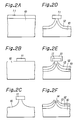
- Figs.2A through 2F are views showing an example of the fabrication process of a field-emission type electron source by performing the micro-miniature processing of a silicon substrate.
- Fig.3 is a sectional view showing a state in which a high vapor-pressure substance layer is formed in the electron source shown in Fig.2.
- a Si-substrate 10 having a resistivity ⁇ of 2 to 3 ⁇ cm was cleaned by the normal RCA cleaning technique.
- the thus cleaned substrate 10 was formed with an oxide film (SiO 2 ) 11 of 3000 ⁇ thick, by the wet-oxidation for 22 min. at 1,100°C, as shown in Fig.2A.
- the formed oxide film 11 was patterned with 3 ⁇ m in diameter at a pitch of 5 ⁇ m using the normal lithographic technique.
- the oxide film 11 was etched by the reactive ion etching (RIE) technique so as to leave only the circular portion of 3 ⁇ m in diameter as shown in Fig.2B.
- RIE reactive ion etching
- Si-substrate 10 was selectively etched under the use of the circular oxide film 11 as a mask.
- the Si-substrate 10 was etched by a depth of 2 ⁇ m.
- the masked part of Si-substrate was shaped into a shape having a vertical section of trapezoid with its base placed horizontally and having an upper-base of 8,000 ⁇ in size.
- wet-oxidation for 34 min. at 1,100°C was effected so that the Si-substrate 10 was formed with an oxide film 12 of 4,000 ⁇ thick on the surface thereof, as shown in Fig.2D.
- a gate electrode 13 was formed by the electron-beam deposition technique using niobium (Nb) as a gate metal so that the resultant electrode was angled 50° relative to a normal of the substrate surface.
- the thickness of the gate electrode 13 was 4000 ⁇ .
- the circular oxide film 11 and the oxide film 12 around the emitter 14 were removed by the reactive ion etching (RIE) technique.
- RIE reactive ion etching
- the electron source thus fabricated by the above process was set together with an anode in the vacuum container, in the same manner as example 1, and the degree of vacuum was elevated to 10 -8 Torr.
- the substrate was heated for ten minutes at 300°C to eject gases out. Since the temperature for the treatment was sufficiently higher than -10°C at which the vapor pressure of S would become 10 -8 Torr, S having covered the emitter was evaporated and ejected out from the surface of the emitter, and pure Si appeared on the surface of the emitter.
- the thus obtained electron source was tested in the condition where the anode was applied with +100 V and a voltage was applied with the cathode negative and the gate electrode positive. As a result, a stable anode-current of 10 ⁇ A was obtained at 60 V.
- a Si-emitter 14 was formed by removing the circular oxide film and the oxide film around the emitter in the same manner as in example 3. Thereafter, tungsten (W) was stacked on the surface of the emitter 14 by the electron-beam deposition technique to form a high-melting point metal layer 16. Further, S was stacked over the high-melting point metal layer 16 by the electron-beam deposition technique to form a high vapor-pressure substance layer 17.
- the configuration is shown in Fig.4.
- buffered hydrofluoric acid was used for the removal of the circular oxide film. In this case, the surface of the Si-emitter was more or less oxidized before the vapor-deposition of W, but this did not affect the electron emission since the surface in question was not the surface from which electrons would be emitted.
- the electron source thus fabricated by the above process was set together with an anode in the vacuum container, in the same manner as example 1, and the degree of vacuum was elevated to 10 -8 Torr. In this condition, the electron source was heated for ten minutes at 300°C to eject gases out. Since the temperature for the treatment was sufficiently higher than -10°C at which the vapor pressure of S would become 10 -8 Torr, S having covered the emitter was evaporated and ejected out from the surface of the emitter, the pure W appeared on the surface of the emitter. The thus obtained electron source was tested in the condition where the anode was applied with +100 V and a voltage was applied with the cathode negative and the gate electrode positive. As a result, a stable anode-current of 1 mA was obtained at 60 V.
- the emitter surface is covered with a high vapor-pressure substance, it is possible to prevent the emitter from being oxidized even when the electron source is taken out in the air. Accordingly, the electron source can be stored when many electron sources are fabricated at the same time, whereby it is possible to simplify the production process. Since the surface of the emitter can be secured to be clean when the high vapor-pressure substance is evaporated by heating the electron source in a vacuum, the electron source is adapted to be able to emit electrons in a short period of time after the fabrication. As a result, it is possible to reduce the cost of the device as well as to improve the reliability of the device.
Landscapes
- Engineering & Computer Science (AREA)
- Manufacturing & Machinery (AREA)
- Cold Cathode And The Manufacture (AREA)
Applications Claiming Priority (2)
| Application Number | Priority Date | Filing Date | Title |
|---|---|---|---|
| JP7780095A JP3239038B2 (ja) | 1995-04-03 | 1995-04-03 | 電界放出型電子源の製造方法 |
| JP77800/95 | 1995-04-03 |
Publications (2)
| Publication Number | Publication Date |
|---|---|
| EP0736891A1 true EP0736891A1 (fr) | 1996-10-09 |
| EP0736891B1 EP0736891B1 (fr) | 1998-09-16 |
Family
ID=13644087
Family Applications (1)
| Application Number | Title | Priority Date | Filing Date |
|---|---|---|---|
| EP96302122A Expired - Lifetime EP0736891B1 (fr) | 1995-04-03 | 1996-03-27 | Procédé de fabrication de sources d'électrons du type à émission de champ |
Country Status (3)
| Country | Link |
|---|---|
| US (1) | US5800233A (fr) |
| EP (1) | EP0736891B1 (fr) |
| JP (1) | JP3239038B2 (fr) |
Cited By (2)
| Publication number | Priority date | Publication date | Assignee | Title |
|---|---|---|---|---|
| EP0806785A3 (fr) * | 1996-05-10 | 1998-05-27 | Nec Corporation | Procédé de fabrication d'une cathode froide à émission de champ avec courant d'émission élevé |
| US20160358741A1 (en) * | 2015-05-27 | 2016-12-08 | Kla-Tencor Corporation | System and Method for Providing a Clean Environment in an Electron-Optical System |
Families Citing this family (3)
| Publication number | Priority date | Publication date | Assignee | Title |
|---|---|---|---|---|
| JP5341562B2 (ja) * | 2009-03-04 | 2013-11-13 | 株式会社神戸製鋼所 | イオン源の製造方法、及びこの方法によって製造されたイオン源 |
| US10141155B2 (en) * | 2016-12-20 | 2018-11-27 | Kla-Tencor Corporation | Electron beam emitters with ruthenium coating |
| US10714294B2 (en) * | 2018-05-25 | 2020-07-14 | Kla-Tencor Corporation | Metal protective layer for electron emitters with a diffusion barrier |
Citations (6)
| Publication number | Priority date | Publication date | Assignee | Title |
|---|---|---|---|---|
| US3678325A (en) * | 1969-03-14 | 1972-07-18 | Matsushita Electric Industrial Co Ltd | High-field emission cathodes and methods for preparing the cathodes |
| US4908539A (en) * | 1984-07-24 | 1990-03-13 | Commissariat A L'energie Atomique | Display unit by cathodoluminescence excited by field emission |
| FR2672734A1 (fr) * | 1991-02-08 | 1992-08-14 | Futaba Denshi Kogyo Kk | Element d'emission de champ. |
| US5199917A (en) * | 1991-12-09 | 1993-04-06 | Cornell Research Foundation, Inc. | Silicon tip field emission cathode arrays and fabrication thereof |
| GB2274198A (en) * | 1992-12-11 | 1994-07-13 | Litton Systems Inc | Cross field amplifier |
| US5394006A (en) * | 1994-01-04 | 1995-02-28 | Industrial Technology Research Institute | Narrow gate opening manufacturing of gated fluid emitters |
Family Cites Families (3)
| Publication number | Priority date | Publication date | Assignee | Title |
|---|---|---|---|---|
| US5089292A (en) * | 1990-07-20 | 1992-02-18 | Coloray Display Corporation | Field emission cathode array coated with electron work function reducing material, and method |
| JP2728813B2 (ja) * | 1991-10-02 | 1998-03-18 | シャープ株式会社 | 電界放出型電子源及びその製造方法 |
| US5186670A (en) * | 1992-03-02 | 1993-02-16 | Micron Technology, Inc. | Method to form self-aligned gate structures and focus rings |
-
1995
- 1995-04-03 JP JP7780095A patent/JP3239038B2/ja not_active Expired - Lifetime
-
1996
- 1996-02-09 US US08/599,315 patent/US5800233A/en not_active Expired - Lifetime
- 1996-03-27 EP EP96302122A patent/EP0736891B1/fr not_active Expired - Lifetime
Patent Citations (6)
| Publication number | Priority date | Publication date | Assignee | Title |
|---|---|---|---|---|
| US3678325A (en) * | 1969-03-14 | 1972-07-18 | Matsushita Electric Industrial Co Ltd | High-field emission cathodes and methods for preparing the cathodes |
| US4908539A (en) * | 1984-07-24 | 1990-03-13 | Commissariat A L'energie Atomique | Display unit by cathodoluminescence excited by field emission |
| FR2672734A1 (fr) * | 1991-02-08 | 1992-08-14 | Futaba Denshi Kogyo Kk | Element d'emission de champ. |
| US5199917A (en) * | 1991-12-09 | 1993-04-06 | Cornell Research Foundation, Inc. | Silicon tip field emission cathode arrays and fabrication thereof |
| GB2274198A (en) * | 1992-12-11 | 1994-07-13 | Litton Systems Inc | Cross field amplifier |
| US5394006A (en) * | 1994-01-04 | 1995-02-28 | Industrial Technology Research Institute | Narrow gate opening manufacturing of gated fluid emitters |
Non-Patent Citations (1)
| Title |
|---|
| SPALLAS J P ET AL: "SELF-ALIGNED SILICON FIELD EMISSION CATHODE ARRAYS FORMED BY SELECTIVE, LATERAL THERMAL OXIDATION OF SILICON", JOURNAL OF VACUUM SCIENCE AND TECHNOLOGY: PART B, vol. 11, no. 2, 1 March 1993 (1993-03-01), pages 437 - 440, XP000364846 * |
Cited By (4)
| Publication number | Priority date | Publication date | Assignee | Title |
|---|---|---|---|---|
| EP0806785A3 (fr) * | 1996-05-10 | 1998-05-27 | Nec Corporation | Procédé de fabrication d'une cathode froide à émission de champ avec courant d'émission élevé |
| US5938495A (en) * | 1996-05-10 | 1999-08-17 | Nec Corporation | Method of manufacturing a field emission cold cathode capable of stably producing a high emission current |
| US20160358741A1 (en) * | 2015-05-27 | 2016-12-08 | Kla-Tencor Corporation | System and Method for Providing a Clean Environment in an Electron-Optical System |
| US10692692B2 (en) * | 2015-05-27 | 2020-06-23 | Kla-Tencor Corporation | System and method for providing a clean environment in an electron-optical system |
Also Published As
| Publication number | Publication date |
|---|---|
| JP3239038B2 (ja) | 2001-12-17 |
| US5800233A (en) | 1998-09-01 |
| EP0736891B1 (fr) | 1998-09-16 |
| JPH08273528A (ja) | 1996-10-18 |
Similar Documents
| Publication | Publication Date | Title |
|---|---|---|
| US5469014A (en) | Field emission element | |
| KR100235212B1 (ko) | 전계방출 캐소드 및 그 제조방법 | |
| US6096570A (en) | Field emitter having sharp tip | |
| EP0520780A1 (fr) | Procédé de fabrication d'une matrice d'émetteurs de champ | |
| US5800233A (en) | Process of fabricating field-emission type electron source, electron source fabricated thereby and element structure of electron source | |
| US5620832A (en) | Field emission display and method for fabricating the same | |
| EP0564926B1 (fr) | Cathode froide | |
| JP3546606B2 (ja) | 電界放出素子の製造方法 | |
| JPH03194829A (ja) | 微小真空三極管とその製造方法 | |
| JP3084768B2 (ja) | 電界放出型陰極装置 | |
| JP2743794B2 (ja) | 電界放出カソード及び電界放出カソードの製造方法 | |
| JP3502883B2 (ja) | 冷電子放出素子及びその製造方法 | |
| JP3612883B2 (ja) | 冷電子放出素子及びその製造方法 | |
| JP3622406B2 (ja) | 冷電子放出素子及びその製造方法 | |
| JPH08148083A (ja) | フィールドエミッタの表面改質方法 | |
| JP3437007B2 (ja) | 電界放出陰極及びその製造方法 | |
| JP3595821B2 (ja) | 冷電子放出素子及びその製造方法 | |
| JP3945049B2 (ja) | 冷電子放出素子の製造方法 | |
| JPH1012166A (ja) | 電界放出型画像表示装置及びその製造方法 | |
| JP4693980B2 (ja) | 電界電子放出素子の製造方法 | |
| JPH08329832A (ja) | 電子放出素子及びその製造方法 | |
| JP4241766B2 (ja) | 照明ランプ用冷電子放出素子 | |
| KR100246254B1 (ko) | 실리사이드를 에미터와 게이트로 갖는 전계 방출 소자의 제조방법 | |
| KR960010426B1 (ko) | 디스크-엣지형 전계 전자 방출 소자 및 그 제조방법 | |
| KR100289066B1 (ko) | 전도성박막증착공정을이용한원추형전계방출소자의제조방법 |
Legal Events
| Date | Code | Title | Description |
|---|---|---|---|
| PUAI | Public reference made under article 153(3) epc to a published international application that has entered the european phase |
Free format text: ORIGINAL CODE: 0009012 |
|
| AK | Designated contracting states |
Kind code of ref document: A1 Designated state(s): FR GB |
|
| 17P | Request for examination filed |
Effective date: 19961122 |
|
| 17Q | First examination report despatched |
Effective date: 19961223 |
|
| GRAG | Despatch of communication of intention to grant |
Free format text: ORIGINAL CODE: EPIDOS AGRA |
|
| GRAG | Despatch of communication of intention to grant |
Free format text: ORIGINAL CODE: EPIDOS AGRA |
|
| GRAG | Despatch of communication of intention to grant |
Free format text: ORIGINAL CODE: EPIDOS AGRA |
|
| GRAH | Despatch of communication of intention to grant a patent |
Free format text: ORIGINAL CODE: EPIDOS IGRA |
|
| GRAH | Despatch of communication of intention to grant a patent |
Free format text: ORIGINAL CODE: EPIDOS IGRA |
|
| GRAA | (expected) grant |
Free format text: ORIGINAL CODE: 0009210 |
|
| AK | Designated contracting states |
Kind code of ref document: B1 Designated state(s): FR GB |
|
| ET | Fr: translation filed | ||
| PLBE | No opposition filed within time limit |
Free format text: ORIGINAL CODE: 0009261 |
|
| STAA | Information on the status of an ep patent application or granted ep patent |
Free format text: STATUS: NO OPPOSITION FILED WITHIN TIME LIMIT |
|
| 26N | No opposition filed | ||
| REG | Reference to a national code |
Ref country code: GB Ref legal event code: IF02 |
|
| PGFP | Annual fee paid to national office [announced via postgrant information from national office to epo] |
Ref country code: GB Payment date: 20130327 Year of fee payment: 18 Ref country code: FR Payment date: 20130325 Year of fee payment: 18 |
|
| GBPC | Gb: european patent ceased through non-payment of renewal fee |
Effective date: 20140327 |
|
| REG | Reference to a national code |
Ref country code: FR Ref legal event code: ST Effective date: 20141128 |
|
| PG25 | Lapsed in a contracting state [announced via postgrant information from national office to epo] |
Ref country code: FR Free format text: LAPSE BECAUSE OF NON-PAYMENT OF DUE FEES Effective date: 20140331 Ref country code: GB Free format text: LAPSE BECAUSE OF NON-PAYMENT OF DUE FEES Effective date: 20140327 |