EP0738925A2 - Masque pour l'ajustement de la largeur de ligne d'un motif de photoréserve - Google Patents
Masque pour l'ajustement de la largeur de ligne d'un motif de photoréserve Download PDFInfo
- Publication number
- EP0738925A2 EP0738925A2 EP96301227A EP96301227A EP0738925A2 EP 0738925 A2 EP0738925 A2 EP 0738925A2 EP 96301227 A EP96301227 A EP 96301227A EP 96301227 A EP96301227 A EP 96301227A EP 0738925 A2 EP0738925 A2 EP 0738925A2
- Authority
- EP
- European Patent Office
- Prior art keywords
- region
- pattern
- mask
- transmittance
- photoresist
- Prior art date
- Legal status (The legal status is an assumption and is not a legal conclusion. Google has not performed a legal analysis and makes no representation as to the accuracy of the status listed.)
- Withdrawn
Links
Images


Classifications
-
- G—PHYSICS
- G03—PHOTOGRAPHY; CINEMATOGRAPHY; ANALOGOUS TECHNIQUES USING WAVES OTHER THAN OPTICAL WAVES; ELECTROGRAPHY; HOLOGRAPHY
- G03F—PHOTOMECHANICAL PRODUCTION OF TEXTURED OR PATTERNED SURFACES, e.g. FOR PRINTING, FOR PROCESSING OF SEMICONDUCTOR DEVICES; MATERIALS THEREFOR; ORIGINALS THEREFOR; APPARATUS SPECIALLY ADAPTED THEREFOR
- G03F1/00—Originals for photomechanical production of textured or patterned surfaces, e.g., masks, photo-masks, reticles; Mask blanks or pellicles therefor; Containers specially adapted therefor; Preparation thereof
- G03F1/26—Phase shift masks [PSM]; PSM blanks; Preparation thereof
- G03F1/32—Attenuating PSM [att-PSM], e.g. halftone PSM or PSM having semi-transparent phase shift portion; Preparation thereof
-
- G—PHYSICS
- G03—PHOTOGRAPHY; CINEMATOGRAPHY; ANALOGOUS TECHNIQUES USING WAVES OTHER THAN OPTICAL WAVES; ELECTROGRAPHY; HOLOGRAPHY
- G03F—PHOTOMECHANICAL PRODUCTION OF TEXTURED OR PATTERNED SURFACES, e.g. FOR PRINTING, FOR PROCESSING OF SEMICONDUCTOR DEVICES; MATERIALS THEREFOR; ORIGINALS THEREFOR; APPARATUS SPECIALLY ADAPTED THEREFOR
- G03F7/00—Photomechanical, e.g. photolithographic, production of textured or patterned surfaces, e.g. printing surfaces; Materials therefor, e.g. comprising photoresists; Apparatus specially adapted therefor
- G03F7/70—Microphotolithographic exposure; Apparatus therefor
- G03F7/70058—Mask illumination systems
- G03F7/70191—Optical correction elements, filters or phase plates for controlling intensity, wavelength, polarisation, phase or the like
-
- G—PHYSICS
- G03—PHOTOGRAPHY; CINEMATOGRAPHY; ANALOGOUS TECHNIQUES USING WAVES OTHER THAN OPTICAL WAVES; ELECTROGRAPHY; HOLOGRAPHY
- G03F—PHOTOMECHANICAL PRODUCTION OF TEXTURED OR PATTERNED SURFACES, e.g. FOR PRINTING, FOR PROCESSING OF SEMICONDUCTOR DEVICES; MATERIALS THEREFOR; ORIGINALS THEREFOR; APPARATUS SPECIALLY ADAPTED THEREFOR
- G03F1/00—Originals for photomechanical production of textured or patterned surfaces, e.g., masks, photo-masks, reticles; Mask blanks or pellicles therefor; Containers specially adapted therefor; Preparation thereof
- G03F1/50—Mask blanks not covered by G03F1/20 - G03F1/34; Preparation thereof
-
- H—ELECTRICITY
- H10—SEMICONDUCTOR DEVICES; ELECTRIC SOLID-STATE DEVICES NOT OTHERWISE PROVIDED FOR
- H10P—GENERIC PROCESSES OR APPARATUS FOR THE MANUFACTURE OR TREATMENT OF DEVICES COVERED BY CLASS H10
- H10P76/00—Manufacture or treatment of masks on semiconductor bodies, e.g. by lithography or photolithography
- H10P76/20—Manufacture or treatment of masks on semiconductor bodies, e.g. by lithography or photolithography of masks comprising organic materials
- H10P76/204—Manufacture or treatment of masks on semiconductor bodies, e.g. by lithography or photolithography of masks comprising organic materials of organic photoresist masks
- H10P76/2041—Photolithographic processes
Definitions
- the present invention relates to a mask, and, more particularly, to a mask for adjusting line width of a photoresist pattern according to position on a semiconductor device.
- FIG. 1 illustrates the above coating step, which relate to both the present invention and conventional processes.
- the photoresist when photoresist is coated on a semiconductor substrate 1 where chips 3 are regularly arrayed in a pattern formation process, the photoresist is coated evenly on the surface of semiconductor substrate 1. It is spread radially, as indicated by the arrows in FIG. 1, since in a normal process semiconductor substrate 1 rotates.
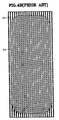
- FIG. 2 is a cross-section of semiconductor substrate 1 coated according to Fig. 1 with the photoresist around an uneven region.
- the coated surface of photoresist 7 becomes relatively planar.
- the coated photoresist has varying thickness according to the position on the substrate due to the sharp change of the relief (degree of unevenness) around the corners of the lower pattern. That is, as shown in FIG. 2, when compared with the thickness of the photoresist on plane surfaces 9 and 12, the thickness of the photoresist on the sunken portion 10 of the uneven region is greater, and that of the photoresist on protruding portion 11 of the uneven region is less.
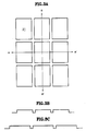
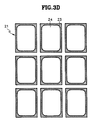
- FIGS. 3A to 3D are views illustrating a semiconductor substrate according to Fig. 2 exhibiting regularly formed unevenness being coated with the photoresist.
- FIGS. 4A and 4B are views illustrating a photolithography procedure according to the conventional technique.
- FIG. 4A shows a mask having a pattern form to be applied to block 21 of FIG. 3D.
- the mask has a constant line width on a transparent substrate and is formed in a regularly arrayed shielding pattern 31.
- the photoresist pattern of FIG. 4B is formed, since the thickness of the photoresist is thin in first region 23. That is, the line width of a first region pattern 33 formed around first region 23 where the thickness of the photoresist is thin is smaller than that of second region pattern 34 formed around second region 24.
- the conventional method for forming the pattern has disadvantages in that the photoresist pattern does not maintain constant line width as the shielding pattern formed on the mask, and the line width of the first region pattern becomes narrow in the first region where the thickness of the photoresist is thin. Further, such variations in line width cannot be tolerated when the pattern of a semiconductor device is very small. In more severe cases, the pattern becomes excessively narrow, crooked or even severed.
- a mask used in photolithography comprising: a transparent substrate; a light-shielding pattern for defining a transmitting region on the transparent substrate; and a transmittance adjusting film pattern disposed in a portion of a transmitting region for increasing transmittance of a second transmitting region to be transferred to a second region compared with a first transmitting region to be transferred to a first region, when the thickness of photoresist in the second region is thicker than that in the first region on the semiconductor substrate where the light-shielding pattern is transferred.
- a mask used in photolithography comprising: a transparent substrate; a light-shielding pattern for defining a transmitting region on the transparent substrate; and a transmittance adjusting film pattern for reducing transmittance of a transmitting region being transferred to a semiconductor substrate through a portion having greater lens aberration of an exposing apparatus.
- the transmittance of the transmittance adjusting film pattern is congruous or variable between 3-97% according to the position on the mask, and that transmittance adjusting film pattern is formed of a material selected from the group consisting of chromium (Cr), molybdenum (Mo), MoSi, MoSiO, MoSiON, CrO, CrON, amorphous carbon, dyed organic spin-on glass (SOG) and photoresist.
- the present invention utilizes the feature that line width of a photoresist pattern varies according to the change in light intensity. Accordingly, the above problem can be solved by exposing photoresist with light intensity adjusted to correspond to each unevenness.
- the light intensity for exposure can be adjusted easily by forming a transmittance adjusting film pattern in a transmitting region of a portion where light intensity is to be adjusted in a mask used for pattern formation.
- FIG. 5A shows a mask used in a first embodiment of the present invention
- FIG. 5B is a photoresist pattern formed by using the mask.
- the mask used in the first embodiment for pattern formation includes shield pattern 31 and transmittance adjusting film pattern 32.
- Transmittance adjusting film pattern 32 has a function of reducing the light intensity exposing a first region 23 of FIG. 3D.
- a photoresist pattern having closely consistent line width is formed as shown in FIG. 5B.
- Transmittance adjusting film pattern 32 is not restricted here to the shape of first region 23, and transmittance may be selected between 3-97%, as required. That is, the line width change of the photoresist pattern formed by using the mask can be adjusted within an allowable range in designing a semiconductor device.
- transmittance adjusting film pattern 32 may be formed of chromium (Cr), molybdenum (Mo), MoSi, MoSiO, MoSiON, CrO, CrON, amorphous carbon, or dyed organic spin-on glass (SOG).
- FIGS. 6A to 6C are views for explaining a method according to the present invention of adjusting line width change of a photoresist pattern generated by lens aberration of an exposing apparatus.
- FIG. 6A shows a third region 43 indicating a part of a lens field 41 where the lens aberration is greater.
- a third region 43 exhibiting greater lens aberration is used for the corners of chip pattern 45.
- light intensity at the portion exposed through third region 43 becomes greater than the other portions, which is undesirable.
- FIG. 6B shows a mask which includes the transmittance adjusting film pattern for adjusting light intensity of a portion corresponding to the third region.
- This mask is made in the same method that is employed in making that of FIG. 5A.
- FIG. 6C shows the arrangement of the transmittance adjusting film pattern at the mask, if the greater lens aberration portion is formed asymmetrically.
- FIGS. 7A and 7B are views respectively showing a result of comparing the conventional method and that of the present invention with respect to an unevenness having the structure of FIG. 2.
- plane portion patterns 59 and 62 formed on plane region 9 and 12 a lower portion pattern 60 formed on sunken portion 10 where the thickness of the photoresist is thick, and a protruded portion pattern 61 formed on protruding portion 11 where the thickness of the photoresist is thin, each exhibit different line widths. Furthermore, a bridge may occur between lower region patterns 60.
- plane region patterns 59a and 62a, a lower region pattern 60a and a protruding region pattern 61a all have the same line width.
- first mask 51a includes first and second transmittance adjusting film patterns 53 and 54. Accordingly, light passed through portions having different transmittances has different intensities. That is, the light intensity exposing lower region 10 is the highest; that exposing protruding region 11 is the lowest; those exposing plane regions 9 and 12 fall between.
- transmittance of first and second transmittance adjusting film patterns 53 and 54 can be made congruous, and a transmittance adjusting film pattern having a different transmittance may be formed in addition when the unevenness becomes more prominent.
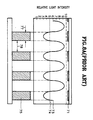
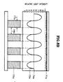
- FIGS. 8A and 8B are graphs indicating the light intensity and the line width change of photoresist pattern in the conventional case and in embodiments of the present invention, respectively.
- Second mask pattern 75 formed to the standard of a threshold energy level 74 of the photoresist has a second mask pattern line width 77 and a second mask pattern interval 78.
- second mask pattern 75a has a second mask pattern line width 77a and second mask pattern interval 78a, these being of the same size.
- the problem of line width change in the photoresist pattern is solved, so that a pattern adapted for use in a highly integrated semiconductor device can be formed by adjusting the light intensity.
Landscapes
- Physics & Mathematics (AREA)
- General Physics & Mathematics (AREA)
- Exposure And Positioning Against Photoresist Photosensitive Materials (AREA)
- Preparing Plates And Mask In Photomechanical Process (AREA)
Applications Claiming Priority (2)
| Application Number | Priority Date | Filing Date | Title |
|---|---|---|---|
| KR1019950009454A KR0144903B1 (ko) | 1995-04-21 | 1995-04-21 | 포토레지스트 패턴의 선폭 조절을 위한 사진 묘화 공정 및 마스크 |
| KR9509454 | 1995-04-21 |
Publications (2)
| Publication Number | Publication Date |
|---|---|
| EP0738925A2 true EP0738925A2 (fr) | 1996-10-23 |
| EP0738925A3 EP0738925A3 (fr) | 1997-04-23 |
Family
ID=19412673
Family Applications (1)
| Application Number | Title | Priority Date | Filing Date |
|---|---|---|---|
| EP96301227A Withdrawn EP0738925A3 (fr) | 1995-04-21 | 1996-02-23 | Masque pour l'ajustement de la largeur de ligne d'un motif de photoréserve |
Country Status (3)
| Country | Link |
|---|---|
| EP (1) | EP0738925A3 (fr) |
| JP (1) | JPH08292551A (fr) |
| KR (1) | KR0144903B1 (fr) |
Cited By (4)
| Publication number | Priority date | Publication date | Assignee | Title |
|---|---|---|---|---|
| US6190840B1 (en) * | 1997-06-18 | 2001-02-20 | Kabushiki Kaisha Toshiba | Resist pattern forming method |
| WO2002001294A1 (fr) * | 2000-06-28 | 2002-01-03 | Koninklijke Philips Electronics N.V. | Appareil et procede permettant de corriger des ecarts de dimension critique dans un photomasque |
| WO2002001295A1 (fr) * | 2000-06-28 | 2002-01-03 | Koninklijke Philips Electronics Nv | Appareil et procede permettant de former un motif de photoresine a dimension critique cible |
| WO2002042846A3 (fr) * | 2000-11-24 | 2003-05-01 | Bookham Technology Plc | Fabrication de circuit integre |
Families Citing this family (2)
| Publication number | Priority date | Publication date | Assignee | Title |
|---|---|---|---|---|
| JP4675504B2 (ja) * | 2001-06-20 | 2011-04-27 | ルネサスエレクトロニクス株式会社 | マスクパターンの設計方法 |
| KR100928512B1 (ko) * | 2007-12-31 | 2009-11-26 | 주식회사 동부하이텍 | 반도체 소자의 제조방법 |
Family Cites Families (9)
| Publication number | Priority date | Publication date | Assignee | Title |
|---|---|---|---|---|
| JPS59155839A (ja) * | 1983-02-25 | 1984-09-05 | Mitsubishi Electric Corp | パタ−ン転写用マスク |
| JPS59178729A (ja) * | 1983-03-30 | 1984-10-11 | Hitachi Ltd | フォトレジストプロセスにおける露光方法 |
| JPS60101931A (ja) * | 1983-11-07 | 1985-06-06 | Sumitomo Electric Ind Ltd | 微細パタ−ン形成法 |
| DE3543014A1 (de) * | 1985-12-05 | 1987-06-11 | Hinrichs Fotowerbung Gmbh | Leuchtkasten fuer diapositive |
| JPS62135837A (ja) * | 1985-12-10 | 1987-06-18 | Matsushita Electric Ind Co Ltd | ホトマスクおよびそれを用いた写真蝕刻法 |
| US4831640A (en) * | 1986-05-14 | 1989-05-16 | The Perkin-Elmer Corporation | Illumination system for x-ray lithography |
| JPS63163855A (ja) * | 1986-12-26 | 1988-07-07 | Mitsubishi Electric Corp | フオトリソグラフイ用マスク |
| JPH04247456A (ja) * | 1991-02-01 | 1992-09-03 | Fujitsu Ltd | 露光用マスク |
| KR950008384B1 (ko) * | 1992-12-10 | 1995-07-28 | 삼성전자주식회사 | 패턴의 형성방법 |
-
1995
- 1995-04-21 KR KR1019950009454A patent/KR0144903B1/ko not_active Expired - Fee Related
-
1996
- 1996-02-23 EP EP96301227A patent/EP0738925A3/fr not_active Withdrawn
- 1996-04-15 JP JP8092797A patent/JPH08292551A/ja active Pending
Cited By (5)
| Publication number | Priority date | Publication date | Assignee | Title |
|---|---|---|---|---|
| US6190840B1 (en) * | 1997-06-18 | 2001-02-20 | Kabushiki Kaisha Toshiba | Resist pattern forming method |
| WO2002001294A1 (fr) * | 2000-06-28 | 2002-01-03 | Koninklijke Philips Electronics N.V. | Appareil et procede permettant de corriger des ecarts de dimension critique dans un photomasque |
| WO2002001295A1 (fr) * | 2000-06-28 | 2002-01-03 | Koninklijke Philips Electronics Nv | Appareil et procede permettant de former un motif de photoresine a dimension critique cible |
| US6590219B1 (en) | 2000-06-28 | 2003-07-08 | Koninklijke Philips Electronics N.V. | Apparatus and method for forming photoresist pattern with target critical dimension |
| WO2002042846A3 (fr) * | 2000-11-24 | 2003-05-01 | Bookham Technology Plc | Fabrication de circuit integre |
Also Published As
| Publication number | Publication date |
|---|---|
| KR0144903B1 (ko) | 1998-08-17 |
| KR960039111A (ko) | 1996-11-21 |
| JPH08292551A (ja) | 1996-11-05 |
| EP0738925A3 (fr) | 1997-04-23 |
Similar Documents
| Publication | Publication Date | Title |
|---|---|---|
| US6566023B2 (en) | Phase shifting circuit manufacture method and apparatus | |
| US5881125A (en) | Attenuated phase-shifted reticle using sub-resolution pattern | |
| KR20020090348A (ko) | 위상편이마스크 및 그 설계방법 | |
| EP0927381A1 (fr) | Procede de fabrication d'un circuit dephaseur et dispositif correspondant | |
| US7393614B2 (en) | Set of masks including a first mask and a second trimming mask with a semitransparent region having a transparency between 20% and 80% to control diffraction effects and obtain maximum depth of focus for the projection of structure patterns onto a semiconductor wafer | |
| TW201403258A (zh) | 半色調光罩及其製造方法,以及採用該半色調光罩之平面顯示器 | |
| US6048650A (en) | Half tone phase shift mask comprising second pattern layer on backside of substrate | |
| EP0738925A2 (fr) | Masque pour l'ajustement de la largeur de ligne d'un motif de photoréserve | |
| US6210841B1 (en) | Approach to increase the resolution of dense line/space patterns for 0.18 micron and below design rules using attenuating phase shifting masks | |
| KR100280035B1 (ko) | 위상쉬프트 포토마스크 | |
| US6635394B2 (en) | Three dimensional mask | |
| JPH06337514A (ja) | マスクおよびパタン形成方法 | |
| US5798192A (en) | Structure of a mask for use in a lithography process of a semiconductor fabrication | |
| US6716558B1 (en) | Transparent phase shift mask for fabrication of small feature sizes | |
| US6383689B1 (en) | Attenuated phase-shift mask and method of manufacturing the same | |
| US5747196A (en) | Method of fabricating a phase-shift photomask | |
| JP3485071B2 (ja) | フォトマスク及び製造方法 | |
| JP2877193B2 (ja) | フォトマスク | |
| US6933085B1 (en) | Transparent phase shift mask for fabrication of small feature sizes | |
| US20020177047A1 (en) | Photomask and method for manufacturing the same | |
| TW386179B (en) | Method for forming pattern in semiconductor device, mask used in method and method for manufacturing mask | |
| KR0166846B1 (ko) | 반도체 마스크 및 그의 제조방법 | |
| JP3243043B2 (ja) | パターン形成方法 | |
| KR100560662B1 (ko) | 마스크 및 그 제조방법 | |
| JPH07230160A (ja) | 位相シフトマスク |
Legal Events
| Date | Code | Title | Description |
|---|---|---|---|
| PUAI | Public reference made under article 153(3) epc to a published international application that has entered the european phase |
Free format text: ORIGINAL CODE: 0009012 |
|
| AK | Designated contracting states |
Kind code of ref document: A2 Designated state(s): DE FR GB |
|
| PUAL | Search report despatched |
Free format text: ORIGINAL CODE: 0009013 |
|
| AK | Designated contracting states |
Kind code of ref document: A3 Designated state(s): DE FR GB |
|
| 17P | Request for examination filed |
Effective date: 19970910 |
|
| 17Q | First examination report despatched |
Effective date: 19980612 |
|
| STAA | Information on the status of an ep patent application or granted ep patent |
Free format text: STATUS: THE APPLICATION IS DEEMED TO BE WITHDRAWN |
|
| 18D | Application deemed to be withdrawn |
Effective date: 20000211 |