EP0740234A2 - Circuit de mesure de delta-T - Google Patents
Circuit de mesure de delta-T Download PDFInfo
- Publication number
- EP0740234A2 EP0740234A2 EP96302531A EP96302531A EP0740234A2 EP 0740234 A2 EP0740234 A2 EP 0740234A2 EP 96302531 A EP96302531 A EP 96302531A EP 96302531 A EP96302531 A EP 96302531A EP 0740234 A2 EP0740234 A2 EP 0740234A2
- Authority
- EP
- European Patent Office
- Prior art keywords
- integrator
- voltage
- circuit
- time
- measurement
- Prior art date
- Legal status (The legal status is an assumption and is not a legal conclusion. Google has not performed a legal analysis and makes no representation as to the accuracy of the status listed.)
- Granted
Links
- 238000005259 measurement Methods 0.000 title claims abstract description 40
- 238000005070 sampling Methods 0.000 claims abstract description 17
- 238000012937 correction Methods 0.000 claims abstract description 8
- 238000000034 method Methods 0.000 claims abstract description 5
- 239000003990 capacitor Substances 0.000 claims description 20
- 238000012546 transfer Methods 0.000 claims description 5
- 230000009466 transformation Effects 0.000 abstract description 2
- 238000010586 diagram Methods 0.000 description 8
- 238000004519 manufacturing process Methods 0.000 description 7
- 230000006870 function Effects 0.000 description 4
- 238000006243 chemical reaction Methods 0.000 description 2
- 230000003750 conditioning effect Effects 0.000 description 2
- 238000012986 modification Methods 0.000 description 2
- 230000004048 modification Effects 0.000 description 2
- 230000008569 process Effects 0.000 description 2
- 238000012545 processing Methods 0.000 description 2
- 230000009471 action Effects 0.000 description 1
- 238000013459 approach Methods 0.000 description 1
- 238000013329 compounding Methods 0.000 description 1
- 238000007796 conventional method Methods 0.000 description 1
- 230000003111 delayed effect Effects 0.000 description 1
- 230000001419 dependent effect Effects 0.000 description 1
- 238000011161 development Methods 0.000 description 1
- 230000000977 initiatory effect Effects 0.000 description 1
- 238000000691 measurement method Methods 0.000 description 1
- 238000012360 testing method Methods 0.000 description 1
Images


Classifications
-
- G—PHYSICS
- G04—HOROLOGY
- G04F—TIME-INTERVAL MEASURING
- G04F10/00—Apparatus for measuring unknown time intervals by electric means
- G04F10/10—Apparatus for measuring unknown time intervals by electric means by measuring electric or magnetic quantities changing in proportion to time
Definitions
- This invention relates generally to circuits for measuring small incremental time, and in particular to a circuit for accurately measuring the time difference between a trigger point and a sample pulse in a digital oscilloscope.
- the horizontal time base sweep always start at substantially the same point on a waveform. This is achieved in analog oscilloscopes by generating a trigger to initiate a new sweep when the input signal passes through a selected triggering level, and the processed signal is delayed slightly to allow the sweep circuits to be initiated. In digital oscilloscopes, however, the input signal is broken up by a sampling clock into a series of evenly spaced instantaneous-amplitude points on the waveform, and the point on the signal at which a trigger is generated and the points on the signal at which samples are taken are unrelated to each other.
- the digital oscilloscope continues to take samples and thus acquire input signals until a trigger comes along, either starting or stopping the waveform acquisition.
- the trigger point and the sample clock are completely unrelated and are asynchronous, resulting in a high probability of the trigger point falling between two sampling clock pulse edges.
- This problem becomes increasingly significant at higher signal frequencies that approach the sampling clock frequency.
- the small differential time between the trigger point and a sampling clock edge known as ⁇ T (delta-T)
- ⁇ T delta-T
- a method of and apparatus for measuring very short time periods, or time differences between two electrical events, such as the delta-T between a trigger point and a preceding or subsequent clock pulse edge comprises an integrator whose output sweep ramp is started on a clock pulse edge and stopped on a trigger pulse (or started on a trigger pulse and stopped on a clock pulse edge) to perform as a time-to-voltage converter.
- the output sweep ramp is normalized to a fixed differential time and fixed differential amplitude, and thus providing a fixed slope to ensure an accurate time-to-voltage transfer function irrespective of the tolerance of the integrator capacitor or the tolerance of the current source fumishing charge current to the capacitor.
- the output of the integrator is applied to an analog-to-digital converter which produces digital data representative of the measured time, thus providing an accurate delta-T measurement circuit.
- a reference circuit responsive to a predetermined differential time and a predetermined differential voltage provides a normalized transfer function for the delta-T measurement integrator.
- a reference integrator substantially identical to the delta-T measurement integrator circuit is operated at the same timing as the delta-T integrator to provide reference sweeps.
- the peak value of each reference sweep is sampled by a sample-and-hold circuit, and used to generate a DC control voltage for an error amplifier that compares the DC control voltage with a predetermined reference voltage.
- the error amplifier produces an output current that is used as the charging current for both integrators. Since the error amplifier produces whatever current is required by the reference integrator to normalize its ramp to a peak value of the reference voltage, the delta-T integrator is likewise normalized to the same voltage.
- accurate time differential measurements may be made independent of manufacturing process deviations and component tolerances.
- Fig. 1 a block diagram of the acquisition system of a digital oscilloscope that incorporates a delta-T measurement system in accordance with the present invention
- Fig. 2 is a waveform diagram to explain the system of Fig. 1.
- An input analog signal is applied via an input terminal 10 to a signal conditioning circuit 12, which includes conventional input attenuators and gain-switched preamplifiers to adjust the signal amplitude to a level suitable for processing by a track-and-hold circuit 14 and analog-to-digital converter (ADC) 16.
- the track-and-hold circuit 14 and ADC 16 convert the instantaneous amplitudes (represented by large dots in Fig. 2) of the analog signal to digital representations at a rate established by sampling clock 18.
- the digital representations, or samples as they are also known, are stored in an acquisition waveform memory 20 for further processing and subsequent display by a processor 22 and display system 24.
- the analog input signal is also applied from the signal conditioning circuit 12 to a trigger circuit 30, which may suitably include a conventional trigger comparator which generates a trigger signal when the input signal passes through a selected trigger level.
- a trigger circuit 30 which may suitably include a conventional trigger comparator which generates a trigger signal when the input signal passes through a selected trigger level.
- the trigger signal and clock signals from the sampling clock 18 are passed to a trigger logic circuit 32, which issues a valid trigger to the processor 22 to either start or stop waveform acquisition, depending on the selected operating mode.
- the trigger logic circuit 32 also develops timing signals from the trigger and clock signal, and applies them to a delta-T measuring circuit 34.
- the measured differential time is then sent to processor 22 to establish the time positions of the acquired digital samples.
- since the clock period is known, it is not critical as to which side of the trigger signal the delta-T measurement is made, as long as the system used is consistent to ensure that the acquired samples appear in their correct time positions.
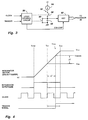
- Fig. 3 shows a partial delta-T measurement circuit 34 in simplified form
- Fig. 4 shows waveform diagrams to explain the circuit of Fig. 4.
- Clock signals which are derived from the sampling clock, and therefore occur at the sampling clock rate, are applied to a logic control circuit 50 along with the trigger signal.
- the sampling clock operates at a 25-megahertz rate, resulting in a 40-nanosecond clock period.
- Logic control circuit 50 develops a T START signal from a clock edge, and a T STOP signal from the trigger signal, developing an integrator gate pulse whose duration is from T START to T STOP .
- the time T STOP falls at some point between times T MIN and T MAX in Fig. 4.
- the period T MAX - T MIN is equal to one clock period.
- the incremental time from T MIN to T STOP is the delta-T being measured.
- the integrator gate pulse is applied to a delta-T integrator 52 comprising a current source 54 and a capacitor 56 to gate the integrator on for the time period from T START to T STOP .
- the integrator gate pulse closes a switch 58 and opens a switch 60, connecting the current source 54 to the capacitor 56.
- the ramp produced by the integrator Since accurate time-to-voltage measurements are being made, it is important that the ramp produced by the integrator always have a slope that is determined by a known time and a known amplitude, and always be the same slope for every measurement. In order for delta-T to be accurately transformed to delta-V, the slope, and hence, the transfer function, must always be the same.
- integrated-circuit manufacturing processes result in capacitors that may have tolerances within ⁇ 20%, which will result in imprecise measurements.
- current generators in such integrated circuits may have tolerance that are also within ⁇ 20%, further compounding delta-T measurement errors. It can readily be discerned that if the ramp in Fig.
- the delta-T to delta-V transformation would be erroneous.
- these tolerances are corrected by automatically and dynamically normalizing the integrator ramp voltage to a predetermined amplitude for a given known time period.
- the word "normalize” used herein has the ordinary meaning as understood in the electronic test and measurement industry, and is defined in the IEEE Standard Dictionary of Electrical and Electronic Terms, published as ANSI/IEEE Standard 100-1988, as "to adjust a measured parameter to a value acceptable to an instrument or measurement technique.”
- the ramp is normalized to the voltage window of an analog-to-digital converter, and is always the same for every measurement.
- Fig. 5 shows a detailed block diagram of a delta-T measurement circuit including a circuit to automatically and dynamically normalize the integrator ramp voltage to a predetermined slope in accordance with the present invention.
- Logic control circuit 50, delta-T integrator 52, and ADC 62 are substantially as described in connection with Fig. 3, with the exception that the current for the delta-T integrator 52 is corrected to normalize the ramp voltage for the delta-T sweep as shown in Fig. 4.
- the necessary current correction for the delta-T integrator is provided by a reference circuit having a substantially identical integrator to be described in conjunction with the waveforms shown in Fig. 6.
- a timing generator 70 receives a reference clock signal which has the same timing as the sample clock received by logic control circuit 50, and continuously generates R START , R STOP , and sample pulses in the sequence shown in Fig. 6.
- a reference-T integrator 72 which is substantially identical to delta-T integrator 52 and is preferably located within the same integrated circuit and thus has been subjected to the same manufacturing process, generates reference sweeps whose time duration is equal to two complete clock cycles and therefore is the same time duration as the delta-T sweep.
- a sample-and-hold circuit 74 takes a sample of the peak voltage.
- Sample-and-hold circuit 74 acts like a rectifier, but it is fast acting, avoids an extra dominant pole in the control loop, and isolates the following control circuitry from the integrator output.
- the sample-and hold output voltage (SH DC output) is applied to an RC network comprising resistor 76 and capacitor 78, producing an RC-controlled DC control voltage that is applied to the inverting input of a loop amplifier 80 that also has a reference voltage applied to its non-inverting input.
- the RC network 76-78 also provides a well-fixed dominant pole for the control loop.
- the reference voltage V REF is equal to V MAX to set the peak values of ramp voltage outputs of integrators 52 and 72.
- Loop amplifier 80 converts the voltage difference at its inputs to a current which is added to a current provided by current generator 82 to be applied to integrators 52 and 72 as charging current for the respective integrator capacitors.
- the waveforms of Fig. 6 represent action of the reference circuit from power-up, that is, when power is first applied to the instrument.
- the peak value of the ramp exceeds V REF , causing the sampled voltage to in turn produce a DC control voltage at the junction of resistor 76 and capacitor 78 of a magnitude sufficient to reduce the current output of amplifier 80.
- the peak value of the ramp is reduced because of the reduced charging current furnished by amplifier 80.
- the sampled voltage and DC control voltage are lowered, increasing the current output of amplifier 80 so that on the third reference-T sweep cycle, the peak value of the ramp again exceeds V REF , but not by as much as it did on the first cycle.
- the peak values of the reference-T ramps converge to V REF , with amplifier 80 providing whatever current is necessary to correct process and component deviations.
- This in turn causes the delta-T ramps to be normalized to a peak value of V MAX . Since the deviations of the two integrators 52 and 72 are the same, V REF V MAX .
- amplifier 80 could generate a control voltage to control current generators internal to integrators 52 and 72 with substantially the same results. It is therefore contemplated that the appended claims will cover all such changes and modifications as fall within the true scope of the invention.
Landscapes
- Physics & Mathematics (AREA)
- General Physics & Mathematics (AREA)
- Measurement Of Resistance Or Impedance (AREA)
- Analogue/Digital Conversion (AREA)
- Measurement Of Current Or Voltage (AREA)
Applications Claiming Priority (2)
| Application Number | Priority Date | Filing Date | Title |
|---|---|---|---|
| US43001595A | 1995-04-27 | 1995-04-27 | |
| US430015 | 1995-04-27 |
Publications (3)
| Publication Number | Publication Date |
|---|---|
| EP0740234A2 true EP0740234A2 (fr) | 1996-10-30 |
| EP0740234A3 EP0740234A3 (fr) | 1997-07-09 |
| EP0740234B1 EP0740234B1 (fr) | 2002-09-18 |
Family
ID=23705723
Family Applications (1)
| Application Number | Title | Priority Date | Filing Date |
|---|---|---|---|
| EP96302531A Expired - Lifetime EP0740234B1 (fr) | 1995-04-27 | 1996-04-10 | Circuit de mesure de delta-T |
Country Status (3)
| Country | Link |
|---|---|
| US (1) | US5790480A (fr) |
| EP (1) | EP0740234B1 (fr) |
| DE (1) | DE69623683T2 (fr) |
Cited By (4)
| Publication number | Priority date | Publication date | Assignee | Title |
|---|---|---|---|---|
| US5836004A (en) * | 1997-01-07 | 1998-11-10 | Industrial Technology Research Institute | Differential mode time to digital converter |
| CN102818940A (zh) * | 2011-06-06 | 2012-12-12 | 泰利斯意大利股份公司 | 具有高时间精度的用信号检测阈值跨越瞬间的方法 |
| CN104466890A (zh) * | 2014-12-05 | 2015-03-25 | 青岛鼎信通讯股份有限公司 | 一种过流保护控制电路 |
| CN105222744A (zh) * | 2014-06-26 | 2016-01-06 | 约翰内斯·海德汉博士有限公司 | 用于在位置测量设备中产生触发信号的装置和方法以及与此相关的位置测量设备 |
Families Citing this family (11)
| Publication number | Priority date | Publication date | Assignee | Title |
|---|---|---|---|---|
| US6091671A (en) * | 1999-07-14 | 2000-07-18 | Guide Technology, Inc. | Time interval analyzer having interpolator with constant current capacitor control |
| US6181649B1 (en) * | 1999-07-14 | 2001-01-30 | Guide Technology, Inc. | Time interval analyzer having current boost |
| US20030016403A1 (en) * | 2001-07-13 | 2003-01-23 | Carlson Gerard J. | Characterization of a scan line produced from a facet of a scanning device |
| US7460441B2 (en) * | 2007-01-12 | 2008-12-02 | Microchip Technology Incorporated | Measuring a long time period |
| US7843771B2 (en) * | 2007-12-14 | 2010-11-30 | Guide Technology, Inc. | High resolution time interpolator |
| KR101258877B1 (ko) * | 2009-11-26 | 2013-04-29 | 한국전자통신연구원 | 클럭 검출기 및 이를 이용한 바이어스 전류 조절 회로 |
| KR20120069349A (ko) * | 2010-12-20 | 2012-06-28 | 삼성전자주식회사 | 스위칭 손실을 줄이는 직류-직류 전압 변환기, 상기 직류-직류 전압 변환기를 포함하는 무선전력 수신 장치 |
| FR3089722B1 (fr) | 2018-12-11 | 2021-06-25 | Commissariat Energie Atomique | Calibration d'un circuit retardateur |
| US20210278441A1 (en) * | 2020-03-04 | 2021-09-09 | Tektronix, Inc. | Identifying one or more acquisitions of interest using visual qualification |
| CN113358144A (zh) * | 2020-03-04 | 2021-09-07 | 特克特朗尼克公司 | 使用视觉鉴定来标识一个或多个感兴趣的采集 |
| WO2026080223A1 (fr) * | 2024-10-07 | 2026-04-16 | Microchip Technology Incorporated | Systèmes et procédés de mesure de temps ou de capacité |
Family Cites Families (9)
| Publication number | Priority date | Publication date | Assignee | Title |
|---|---|---|---|---|
| FR2134112B1 (fr) * | 1971-04-20 | 1974-03-22 | Sodern | |
| JPS52123670A (en) * | 1976-04-09 | 1977-10-18 | Takeda Riken Ind Co Ltd | Digital frequency measuring device |
| DE2855819C3 (de) * | 1977-12-26 | 1981-05-21 | Takeda Riken Kogyo K.K., Tokyo | Zeitintervall-Meßeinrichtung |
| US4251754A (en) * | 1979-09-04 | 1981-02-17 | Tektronix, Inc. | Digital oscilloscope with reduced jitter due to sample uncertainty |
| US4301360A (en) * | 1979-10-25 | 1981-11-17 | Tektronix, Inc. | Time interval meter |
| US4613950A (en) * | 1983-09-22 | 1986-09-23 | Tektronix, Inc. | Self-calibrating time interval meter |
| US4504155A (en) * | 1984-03-01 | 1985-03-12 | Chip Supply | Time-to-voltage converter |
| US4982350A (en) * | 1987-06-10 | 1991-01-01 | Odetics, Inc. | System for precise measurement of time intervals |
| US5196741A (en) * | 1989-01-25 | 1993-03-23 | Hewlett-Packard Company | Recycling ramp interpolator |
-
1996
- 1996-04-10 EP EP96302531A patent/EP0740234B1/fr not_active Expired - Lifetime
- 1996-04-10 DE DE69623683T patent/DE69623683T2/de not_active Expired - Lifetime
-
1997
- 1997-05-12 US US08/854,864 patent/US5790480A/en not_active Expired - Lifetime
Cited By (7)
| Publication number | Priority date | Publication date | Assignee | Title |
|---|---|---|---|---|
| US5836004A (en) * | 1997-01-07 | 1998-11-10 | Industrial Technology Research Institute | Differential mode time to digital converter |
| CN102818940A (zh) * | 2011-06-06 | 2012-12-12 | 泰利斯意大利股份公司 | 具有高时间精度的用信号检测阈值跨越瞬间的方法 |
| CN102818940B (zh) * | 2011-06-06 | 2017-01-18 | 泰利斯意大利股份公司 | 具有高时间精度的用信号检测阈值跨越瞬间的方法 |
| CN105222744A (zh) * | 2014-06-26 | 2016-01-06 | 约翰内斯·海德汉博士有限公司 | 用于在位置测量设备中产生触发信号的装置和方法以及与此相关的位置测量设备 |
| CN105222744B (zh) * | 2014-06-26 | 2018-11-20 | 约翰内斯·海德汉博士有限公司 | 用于在位置测量设备中产生触发信号的装置和方法以及与此相关的位置测量设备 |
| CN104466890A (zh) * | 2014-12-05 | 2015-03-25 | 青岛鼎信通讯股份有限公司 | 一种过流保护控制电路 |
| CN104466890B (zh) * | 2014-12-05 | 2017-08-11 | 青岛鼎信通讯股份有限公司 | 一种过流保护控制电路 |
Also Published As
| Publication number | Publication date |
|---|---|
| EP0740234A3 (fr) | 1997-07-09 |
| US5790480A (en) | 1998-08-04 |
| DE69623683D1 (de) | 2002-10-24 |
| DE69623683T2 (de) | 2003-08-07 |
| EP0740234B1 (fr) | 2002-09-18 |
Similar Documents
| Publication | Publication Date | Title |
|---|---|---|
| US5790480A (en) | Delta-T measurement circuit | |
| US4807147A (en) | Sampling wave-form digitizer for dynamic testing of high speed data conversion components | |
| US4799008A (en) | AC level calibration apparatus | |
| EP0330693A1 (fr) | Appareil et procede de comptage de frequences | |
| GB2149988A (en) | Sampling wave-form digitizer for dynamic testing of high speed data conversion components | |
| US5886660A (en) | Time-to-digital converter using time stamp extrapolation | |
| US5287063A (en) | Calibration circuit and method for maximum and minimum value detection apparatus | |
| CN110708047B (zh) | 一种基于tdc芯片测量高速比较器精度的结构及方法 | |
| EP0235911B1 (fr) | Détecteur de niveau pour une forme de l'onde d'un système échantillonneur | |
| US7184908B2 (en) | Calibration method of time measurement apparatus | |
| US4362394A (en) | Time interval measurement arrangement | |
| JPH01232821A (ja) | 傾斜信号校正方法及びデジタル・タイム・ベース回路 | |
| US20030220758A1 (en) | Method for testing an AD-converter | |
| EP3806331B1 (fr) | Oscillateur rc | |
| US4719408A (en) | Apparatus for indicating proper compensation of an adjustable frequency compensation network | |
| US4527907A (en) | Method and apparatus for measuring the settling time of an analog signal | |
| JPH063372A (ja) | ディジタルサンプリングオシロスコープ装置、およびその時間軸誤差の測定方法および校正方法 | |
| CN120263184B (zh) | 一种用于同步降采样的时间插补电路及插补时间修正方法 | |
| JP3239338B2 (ja) | リップルノイズ電圧測定装置 | |
| EP0418614A2 (fr) | Méthode et appareil pour calibrer une ligne de retardement linéaire | |
| EP0101060A2 (fr) | Convertisseur analogique numérique à échelle positionnée | |
| SU1002991A1 (ru) | Устройство дл контрол пороговых уровней радиоэлектронных схем | |
| SU798631A1 (ru) | Способ измерени составл ющихКОМплЕКСНыХ СОпРОТиВлЕНий | |
| Chapman et al. | Conversion of a multichannel analyser into an analogue signal averager | |
| SU661375A1 (ru) | Цифровой интегрирующий измеритель отношени двух посто нных напр жений |
Legal Events
| Date | Code | Title | Description |
|---|---|---|---|
| PUAI | Public reference made under article 153(3) epc to a published international application that has entered the european phase |
Free format text: ORIGINAL CODE: 0009012 |
|
| AK | Designated contracting states |
Kind code of ref document: A2 Designated state(s): DE FR GB |
|
| PUAL | Search report despatched |
Free format text: ORIGINAL CODE: 0009013 |
|
| AK | Designated contracting states |
Kind code of ref document: A3 Designated state(s): DE FR GB |
|
| 17P | Request for examination filed |
Effective date: 19970818 |
|
| 17Q | First examination report despatched |
Effective date: 19980902 |
|
| GRAG | Despatch of communication of intention to grant |
Free format text: ORIGINAL CODE: EPIDOS AGRA |
|
| GRAG | Despatch of communication of intention to grant |
Free format text: ORIGINAL CODE: EPIDOS AGRA |
|
| GRAG | Despatch of communication of intention to grant |
Free format text: ORIGINAL CODE: EPIDOS AGRA |
|
| GRAG | Despatch of communication of intention to grant |
Free format text: ORIGINAL CODE: EPIDOS AGRA |
|
| GRAH | Despatch of communication of intention to grant a patent |
Free format text: ORIGINAL CODE: EPIDOS IGRA |
|
| GRAH | Despatch of communication of intention to grant a patent |
Free format text: ORIGINAL CODE: EPIDOS IGRA |
|
| GRAA | (expected) grant |
Free format text: ORIGINAL CODE: 0009210 |
|
| AK | Designated contracting states |
Kind code of ref document: B1 Designated state(s): DE FR GB |
|
| REG | Reference to a national code |
Ref country code: GB Ref legal event code: FG4D |
|
| REF | Corresponds to: |
Ref document number: 69623683 Country of ref document: DE Date of ref document: 20021024 |
|
| ET | Fr: translation filed | ||
| PLBE | No opposition filed within time limit |
Free format text: ORIGINAL CODE: 0009261 |
|
| STAA | Information on the status of an ep patent application or granted ep patent |
Free format text: STATUS: NO OPPOSITION FILED WITHIN TIME LIMIT |
|
| 26N | No opposition filed |
Effective date: 20030619 |
|
| REG | Reference to a national code |
Ref country code: FR Ref legal event code: PLFP Year of fee payment: 20 |
|
| PGFP | Annual fee paid to national office [announced via postgrant information from national office to epo] |
Ref country code: GB Payment date: 20150427 Year of fee payment: 20 Ref country code: DE Payment date: 20150429 Year of fee payment: 20 |
|
| PGFP | Annual fee paid to national office [announced via postgrant information from national office to epo] |
Ref country code: FR Payment date: 20150417 Year of fee payment: 20 |
|
| REG | Reference to a national code |
Ref country code: DE Ref legal event code: R071 Ref document number: 69623683 Country of ref document: DE |
|
| REG | Reference to a national code |
Ref country code: GB Ref legal event code: PE20 Expiry date: 20160409 |
|
| PG25 | Lapsed in a contracting state [announced via postgrant information from national office to epo] |
Ref country code: GB Free format text: LAPSE BECAUSE OF EXPIRATION OF PROTECTION Effective date: 20160409 |