EP0418614A2 - Méthode et appareil pour calibrer une ligne de retardement linéaire - Google Patents
Méthode et appareil pour calibrer une ligne de retardement linéaire Download PDFInfo
- Publication number
- EP0418614A2 EP0418614A2 EP90116732A EP90116732A EP0418614A2 EP 0418614 A2 EP0418614 A2 EP 0418614A2 EP 90116732 A EP90116732 A EP 90116732A EP 90116732 A EP90116732 A EP 90116732A EP 0418614 A2 EP0418614 A2 EP 0418614A2
- Authority
- EP
- European Patent Office
- Prior art keywords
- voltage
- ramp
- generating
- response
- line
- Prior art date
- Legal status (The legal status is an assumption and is not a legal conclusion. Google has not performed a legal analysis and makes no representation as to the accuracy of the status listed.)
- Withdrawn
Links
Images


Classifications
-
- G—PHYSICS
- G01—MEASURING; TESTING
- G01R—MEASURING ELECTRIC VARIABLES; MEASURING MAGNETIC VARIABLES
- G01R35/00—Testing or calibrating of apparatus covered by the other groups of this subclass
- G01R35/005—Calibrating; Standards or reference devices, e.g. voltage or resistance standards, "golden" references
-
- G—PHYSICS
- G01—MEASURING; TESTING
- G01R—MEASURING ELECTRIC VARIABLES; MEASURING MAGNETIC VARIABLES
- G01R31/00—Arrangements for testing electric properties; Arrangements for locating electric faults; Arrangements for electrical testing characterised by what is being tested not provided for elsewhere
- G01R31/28—Testing of electronic circuits, e.g. by signal tracer
- G01R31/317—Testing of digital circuits
- G01R31/3181—Functional testing
- G01R31/319—Tester hardware, i.e. output processing circuits
- G01R31/31903—Tester hardware, i.e. output processing circuits tester configuration
- G01R31/31908—Tester set-up, e.g. configuring the tester to the device under test [DUT], down loading test patterns
- G01R31/3191—Calibration
Definitions
- This invention relates to electronic testing devices and, more particularly, to a method and apparatus for calibrating linear delay lines in a VLSI tester.
- the time marker signals which are used to form the test signals must be accurately placed within prescribed time intervals.
- the time intervals typically comprise the periods of a system clock signal. It is not uncommon to find system clock periods on the order of 3.2 nanoseconds, and this frequently results in a required marker placement resolution on the order of picoseconds.
- a delay circuit 10 comprises a range digital-to-analog converter (DAC) 14 for converting a digital word into a charging current on a line 18; an integrator 22 for converting the current on line 18 into a ramp voltage on line 26; a delay DAC 30 for converting a digital word into a reference voltage on a line 34; and a comparator 38 for comparing the range voltage on line 26 with the reference voltage on line 34 and for producing a signal on a line 42 when the range voltage matches the reference voltage.
- DAC digital-to-analog converter
- delay circuit 10 Operation of delay circuit 10 may be understood by referring to Figure 2.
- Delay DAC 30 produces a voltage V n on line 34, and range DAC 14 produces a current I c on line 18.
- integrator 22 At the beginning of each system clock period integrator 22 produces an increasing voltage from current I c on line 26.
- the voltage on line 26 matches the reference voltage V n on line 34, and a signal is provided on line 42 for indicating that fact.
- the time T n that it takes for the voltage produced by integrator 22 to reach V n determines the delay from the start of the clock pulse and hence determines the point within the clock period where the timing marker is to be placed.
- the charging current I c , the reference voltage V n or the charging characteristics of integrator 22 may not be precise. For example, if the charging time of integrator 22 is smaller than expected, then, when a current I c ′ ( Figure 2) is provided on line 18, a longer time T n′ elapses before the reference voltage V n is matched. On the other hand, if the charging rate of integrator 22 is faster than expected, then a charging current I c ⁇ causes the voltage on line 26 to increase much faster, and hence a shorter time T n ⁇ elapses before the reference voltage V n is matched. Consequently, the actual range of delay times T n′ or T n ⁇ may vary significantly from the theoretical range of delay time T n , and the circuit will not perform properly.
- the present invention is directed to a method as defined in claim 10 and apparatus as defined in claim 1 for calibrating linear delay lines wherein the charging current provided by a range DAC is automatically adjusted to compensate for any variations from theoretical circuit operating parameters.
- a voltage generator generates a ramp voltage at first and second frequencies.
- a counter counts the number of cycles of the ramp voltages generated at the first and second frequencies, and, based on the difference in the number of ramp voltages counted, the rate of change or slope of the ramp voltage may be adjusted.
- FIG. 3 is a block diagram of a linear delay circuit 50 which includes calibration circuitry according to the present invention.
- a range DAC 54 receives an eight-bit digital word on bit lines 58 and produces therefrom a charging current I1 on a line 62.
- the current on line 62 is communicated to an integrator 66 which typically includes a capacitance for converting the charging current from line 62 into a ramp voltage on line 70.
- the voltage on line 70 is communicated to one input terminal of a comparator 74.
- a delay DAC 78 receives an eight-bit digital word over bit lines 82 and produces therefrom a reference voltage on a line 86.
- the reference voltage on line 86 is communicated to the other input terminal of comparator 74.
- Comparator 74 compares the ramp voltage on line 70 with the reference voltage on line 86 and produces a time marker signal on a line 90 when the voltages match.
- the time marker signal on line 90 is communicated to the reset input terminal of a flip-flop 94 for causing flip-flop 94 to assume a reset state. In this state a low signal appears on the Q output terminal of flip-flop 94 and a high signal appears on the Q output terminal of flip-flop 94.
- flip-flop 94 is in the reset state, the high signal appearing at the Q output terminal of flip-flop terminal 94 is communicated to integrator 66 over a line 98 for discharging the capacitance in integrator 66 and hence reset the ramp voltage on line 70.
- the Q output terminal of flip-flop terminal 94 is coupled to a line 102 which, in turn, is coupled to an integrator 106 and a programmable counter 108.
- Integrator 106 receives a fixed current I f on a line 110 and produces therefrom a ramp voltage on a line 114.
- Line 114 is coupled to one input terminal of a comparator 118.
- the other input terminal of comparator 118 is coupled to a line 122 for receiving a reference voltage V ref .
- Comparator 118 compares the ramp voltage received on line 114 with the reference voltage received on line 122 and provides a time marker signal on a line 126 when the voltages match.
- a control unit 130 controls calibration of the circuit.
- Control unit 130 receives a mode signal on a line 134 for placing circuit 50 in an automatic calibration mode.
- control unit 130 provides signals to counter 108, to a counter/register 138 and to an AND gate 142 over lines 146, 150 and 156, respectively, for enabling the operation of these units.
- control unit 130 couples the time marker signal from line 126 to a line 160 which, in turn, is connected to the set input terminal of flip-flop 94 for placing flip-flop 94 in a set state.
- flip-flop 94 When flip-flop 94 is in a set state, a high signal appears on line 102 for discharging the capacitance in integrator 106.
- flip-flop 94 is converted into a free-running multivibrator by control line 134.
- Counter 108 is programmed to count N cycles of the oscillating frequency of flip-flop 94. While counter 108 is counting it provides a count signal over line 164. The count signal is used in conjunction with control signal line 156 for enabling AND gate 142. The control signals on line 156 enable the up/down counter register 138 to count the number of system clock pulses on line 166 during the period of the count signal on line 164 through the AND gate 142 over line 180. The contents of counter/register 138 are communicated to an adder 174 over bit lines 178. Adder 174 adds (or subtracts) the binary value on lines 178 to the original range DAC input value received from bit lines 182 and produces a new input value on lines 58. The value on lines 58 are looped back to lines 182 to provide an updated input value to adder 174.
- the system clock pulses received on line 166 are square wave pulses having a period T c of 3.2 nanoseconds. Since the delay DAC 78 receives an eight-bit word on line 82, the system clock period T c may be resolved into 256 units of 12.5 picoseconds each. Assume that integrator 66 produces a linear ramp voltage in response to the current I1 from range DAC 54 and that T n is the calibrated time taken to integrate from V 0 to V n when the input of delay DAC 78 is set to n. Assume further that the input word on lines 82 to delay DAC 78 is set to 255 (hex FF) with T 255′ being the corresponding period.
- An objective of range calibration is to set the charging current I1 (set by the range DAC) so that the voltage ramps created by integrator 66 take exactly 3.1875 nanoseconds to reach the reference voltage V255 provided by delay DAC 78.
- I1 I c where I c is the calibrated integrator current set by the range DAC 54.
- I c I1 - dI1.
- flip-flop 94 When circuit 50 is to be calibrated, flip-flop 94 is placed in a set state (Q high and Q low) for enabling integrator 66 to charge in response to the charging current I1 on line 62.
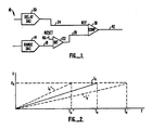
- the input to delay DAC 78 is set to 255 for providing the voltage V255 to comparator 74. Operation of the circuit then proceeds as shown in Figure 4A.
- integrator 66 begins to charge, and the voltage on line 70 linearly varies from V0 to V255 as shown in the upper waveform of Figure 4A.
- the voltage on line 70 matches the reference voltage V255 and a signal is provided on line 90 for resetting flip-flop 94.
- a high signal is provided on line 98 for discharging the capacitance in integrator 66.
- the low signal on line 102 allows integrator 106 to begin charging in response to the fixed current received on line 110 as shown in the lower waveform of Figure 4A.
- the voltage appearing on line 114 matches the reference voltage V ref on line 122, and a time marker signal is produced on line 126.
- control unit 130 couples the signal on line 126 to line 160 for setting flip-flop 94.
- T d1′ between times T4 and T5 before flip-flop 94 sets.
- V ref is chosen so that the interval T w1 between times T3 and T5 is sufficient to allow the capacitance in integrator 66 to completely discharge, so that no duty cycle error is introduced into the calibration.
- the input to the delay DAC is set to 127, and the waveforms shown in Figure 4B are produced.
- T 255′ - T 127′ T 128′
- T 256′ 2 x T 128′
- T 256′ /T c 2 (K1 - K2)/N.
- an eight-bit range DAC 78 is used to provide an adjustment range of ⁇ r% in the charging current I1 for integrator 66. "r" should be chosen to cover for variations in I1 due to process or other tolerances.
- the calibration circuit according to the present invention adds less than two-hundred gates to the circuit shown in Figure 1 and provides for automatic generation of the current correction factor in binary form.
- Calibration is independent of random noise, systematic noise, and timing jitter, since these effects are averaged over N (typically 512 or 1024) cycles.
- Calibration is independent of signal propagation delays (T d1 , T d2 ), charging and discharging characteristics (T w1 and T w2 ) and nonlinearity of the ramp generators. Nonlinearity in the linear portion of the ramp will only affect the linearity of timing resolution, but not range calibration.
- the circuit configuration and functionality of the linear delay line is unaffected by whether the delay line is in calibration or normal mode. As a result, systemic errors are eliminated.
Landscapes
- Physics & Mathematics (AREA)
- General Physics & Mathematics (AREA)
- Engineering & Computer Science (AREA)
- General Engineering & Computer Science (AREA)
- Analogue/Digital Conversion (AREA)
- Pulse Circuits (AREA)
- Measurement Of Unknown Time Intervals (AREA)
- Tests Of Electronic Circuits (AREA)
- Networks Using Active Elements (AREA)
Applications Claiming Priority (2)
| Application Number | Priority Date | Filing Date | Title |
|---|---|---|---|
| US07/410,763 US5014228A (en) | 1989-09-21 | 1989-09-21 | Method and apparatus for calibrating linear delay lines |
| US410763 | 1989-09-21 |
Publications (2)
| Publication Number | Publication Date |
|---|---|
| EP0418614A2 true EP0418614A2 (fr) | 1991-03-27 |
| EP0418614A3 EP0418614A3 (en) | 1992-04-01 |
Family
ID=23626114
Family Applications (1)
| Application Number | Title | Priority Date | Filing Date |
|---|---|---|---|
| EP19900116732 Withdrawn EP0418614A3 (en) | 1989-09-21 | 1990-08-31 | Method and apparatus for calibrating linear delay lines |
Country Status (3)
| Country | Link |
|---|---|
| US (1) | US5014228A (fr) |
| EP (1) | EP0418614A3 (fr) |
| JP (1) | JPH03282272A (fr) |
Cited By (1)
| Publication number | Priority date | Publication date | Assignee | Title |
|---|---|---|---|---|
| US6294542B1 (en) | 1998-04-25 | 2001-09-25 | Boryung Pharmaceutical Co. Ltd. | Pyrimidinone compounds, pharmaceutical compositions containing the compounds and the process for preparing the same |
Families Citing this family (2)
| Publication number | Priority date | Publication date | Assignee | Title |
|---|---|---|---|---|
| GB2229536B (en) * | 1989-03-22 | 1993-04-07 | Ferranti Int Signal | Signal processing apparatus and method |
| CN103513208B (zh) * | 2012-06-29 | 2016-06-29 | 中国船舶重工集团公司第七0九研究所 | 一种皮秒级集成电路测试系统总定时偏差校准的误差补偿方法 |
Family Cites Families (9)
| Publication number | Priority date | Publication date | Assignee | Title |
|---|---|---|---|---|
| US3685048A (en) * | 1970-09-30 | 1972-08-15 | Bendix Corp | Self-calibrating analog to digital converter with predetermined transfer characteristics |
| US3750142A (en) * | 1972-06-09 | 1973-07-31 | Motorola Inc | Single ramp analog to digital converter with feedback |
| DE2626899C3 (de) * | 1976-06-16 | 1979-06-13 | Bizerba-Werke Wilhelm Kraut Kg, 7460 Balingen | Verfahren und Vorrichtung zur Genauigkeitsüberprüfung eines Analog-Digitalwandlers |
| US4238727A (en) * | 1978-12-22 | 1980-12-09 | Systron-Donner Corporation | Digitally programmable apparatus for generating a substantially linear ramp signal |
| US4222107A (en) * | 1979-01-22 | 1980-09-09 | Burr-Brown Research Corporation | Method and apparatus for automatically calibrating a digital to analog converter |
| US4613950A (en) * | 1983-09-22 | 1986-09-23 | Tektronix, Inc. | Self-calibrating time interval meter |
| US4827437A (en) * | 1986-09-22 | 1989-05-02 | Vhl Associates, Inc. | Auto calibration circuit for VLSI tester |
| US4851838A (en) * | 1987-12-18 | 1989-07-25 | Vtc Incorporated | Single chip successive approximation analog-to-digital converter with trimmable and controllable digital-to-analog converter |
| JPH01273427A (ja) * | 1988-04-26 | 1989-11-01 | Mitsubishi Electric Corp | 差分パルス符号変調装置 |
-
1989
- 1989-09-21 US US07/410,763 patent/US5014228A/en not_active Expired - Fee Related
-
1990
- 1990-08-31 EP EP19900116732 patent/EP0418614A3/en not_active Withdrawn
- 1990-09-21 JP JP2254010A patent/JPH03282272A/ja active Pending
Cited By (1)
| Publication number | Priority date | Publication date | Assignee | Title |
|---|---|---|---|---|
| US6294542B1 (en) | 1998-04-25 | 2001-09-25 | Boryung Pharmaceutical Co. Ltd. | Pyrimidinone compounds, pharmaceutical compositions containing the compounds and the process for preparing the same |
Also Published As
| Publication number | Publication date |
|---|---|
| JPH03282272A (ja) | 1991-12-12 |
| US5014228A (en) | 1991-05-07 |
| EP0418614A3 (en) | 1992-04-01 |
Similar Documents
| Publication | Publication Date | Title |
|---|---|---|
| JP3553639B2 (ja) | タイミング調整回路 | |
| US4982350A (en) | System for precise measurement of time intervals | |
| KR101390274B1 (ko) | 집적된 시간 및/또는 캐패시턴스 측정 시스템, 방법 및 장치 | |
| US4962380A (en) | Method and apparatus for calibrating an interleaved digitizer | |
| US6956422B2 (en) | Generation and measurement of timing delays by digital phase error compensation | |
| US7224298B2 (en) | ADC background calibration timing | |
| US7653500B2 (en) | Sequential timebase | |
| US5180971A (en) | Method and apparatus for increasing throughput in random repetitive digitizing systems | |
| EP0740234B1 (fr) | Circuit de mesure de delta-T | |
| US4637733A (en) | High-resolution electronic chronometry system | |
| JP2907033B2 (ja) | タイミング信号発生装置 | |
| US5528186A (en) | Timing generator using digital signals to obtain accurate delay time and high resolution | |
| Raisanen-Ruotsalainen et al. | A time digitizer with interpolation based on time-to-voltage conversion | |
| EP0418614A2 (fr) | Méthode et appareil pour calibrer une ligne de retardement linéaire | |
| JPH01232821A (ja) | 傾斜信号校正方法及びデジタル・タイム・ベース回路 | |
| US5353025A (en) | Methods and apparatus for digitally encoding repetitive analog waveforms | |
| US6914471B2 (en) | Method and apparatus for controlling a dual-slope integrator circuit to eliminate settling time effect | |
| KR950000418B1 (ko) | 시간정보 검출장치 | |
| JPH04196813A (ja) | 遅延回路 | |
| JPH05211442A (ja) | アナログ・ディジタル変換器の試験方法 | |
| GB2227381A (en) | Analogue to digital converters | |
| Raisanen-Ruotsalainen et al. | A BiCMOS time-to-digital converter with time stretching interpolators | |
| Pele et al. | One application of FPGA integrated circuits CMOS camera and LCD display controller design | |
| Wolffenbuttel et al. | Stochastic analog-to-digital converter based on the asynchronous sampling of a reference triangle | |
| Sumner | A sliding scale method to reduce the differential non linearity of a time digitizer |
Legal Events
| Date | Code | Title | Description |
|---|---|---|---|
| PUAI | Public reference made under article 153(3) epc to a published international application that has entered the european phase |
Free format text: ORIGINAL CODE: 0009012 |
|
| AK | Designated contracting states |
Kind code of ref document: A2 Designated state(s): DE FR GB IT NL |
|
| PUAL | Search report despatched |
Free format text: ORIGINAL CODE: 0009013 |
|
| AK | Designated contracting states |
Kind code of ref document: A3 Designated state(s): DE FR GB IT NL |
|
| 17P | Request for examination filed |
Effective date: 19920904 |
|
| 17Q | First examination report despatched |
Effective date: 19931105 |
|
| STAA | Information on the status of an ep patent application or granted ep patent |
Free format text: STATUS: THE APPLICATION IS DEEMED TO BE WITHDRAWN |
|
| 18D | Application deemed to be withdrawn |
Effective date: 19940316 |