EP0740435B1 - Synchronisation von Paritätsbits zur Fehlervermeidung beim Umschalten zwischen einem aktiven und einem stand-by Prozessor - Google Patents
Synchronisation von Paritätsbits zur Fehlervermeidung beim Umschalten zwischen einem aktiven und einem stand-by Prozessor Download PDFInfo
- Publication number
- EP0740435B1 EP0740435B1 EP96302686A EP96302686A EP0740435B1 EP 0740435 B1 EP0740435 B1 EP 0740435B1 EP 96302686 A EP96302686 A EP 96302686A EP 96302686 A EP96302686 A EP 96302686A EP 0740435 B1 EP0740435 B1 EP 0740435B1
- Authority
- EP
- European Patent Office
- Prior art keywords
- data
- parity
- frame
- parity bit
- frames
- Prior art date
- Legal status (The legal status is an assumption and is not a legal conclusion. Google has not performed a legal analysis and makes no representation as to the accuracy of the status listed.)
- Expired - Lifetime
Links
Images


Classifications
-
- H—ELECTRICITY
- H04—ELECTRIC COMMUNICATION TECHNIQUE
- H04L—TRANSMISSION OF DIGITAL INFORMATION, e.g. TELEGRAPHIC COMMUNICATION
- H04L1/00—Arrangements for detecting or preventing errors in the information received
- H04L1/004—Arrangements for detecting or preventing errors in the information received by using forward error control
- H04L1/0056—Systems characterized by the type of code used
- H04L1/0057—Block codes
-
- G—PHYSICS
- G06—COMPUTING OR CALCULATING; COUNTING
- G06F—ELECTRIC DIGITAL DATA PROCESSING
- G06F11/00—Error detection; Error correction; Monitoring
- G06F11/07—Responding to the occurrence of a fault, e.g. fault tolerance
- G06F11/08—Error detection or correction by redundancy in data representation, e.g. by using checking codes
- G06F11/10—Adding special bits or symbols to the coded information, e.g. parity check, casting out 9's or 11's
-
- G—PHYSICS
- G06—COMPUTING OR CALCULATING; COUNTING
- G06F—ELECTRIC DIGITAL DATA PROCESSING
- G06F11/00—Error detection; Error correction; Monitoring
- G06F11/07—Responding to the occurrence of a fault, e.g. fault tolerance
- G06F11/16—Error detection or correction of the data by redundancy in hardware
- G06F11/20—Error detection or correction of the data by redundancy in hardware using active fault-masking, e.g. by switching out faulty elements or by switching in spare elements
-
- H—ELECTRICITY
- H04—ELECTRIC COMMUNICATION TECHNIQUE
- H04L—TRANSMISSION OF DIGITAL INFORMATION, e.g. TELEGRAPHIC COMMUNICATION
- H04L1/00—Arrangements for detecting or preventing errors in the information received
- H04L1/22—Arrangements for detecting or preventing errors in the information received using redundant apparatus to increase reliability
Definitions
- This invention generally relates to a telecommunication network in which active and standby processing apparatus are utilized in the processing and transmission of data. This invention more specifically relates to the switching from the active to the passive apparatus when the data being handled by the apparatus includes hierarchical based parity bits.
- the pair of apparatus is typically referred to as an active and standby apparatus in which the active apparatus is engaged in processing and transmitting user data with the standby apparatus being idle but ready to assume responsibility for processing and transmitting the user data.
- a change of processing from the active to the standby apparatus enables the active apparatus to undergo maintenance and testing to ensure its continued reliability or may occur due to a failure of the active apparatus. It is, of course, desired that a switch over or transition from the active to standby apparatus handling the data transmission be accomplished with minimal, or preferably, no disruption of user data processed by the apparatus.
- parity bits are well known in the art.
- a parity bit or a group of bits are generated by a calculation based on a collection of data to be protected.
- an even parity bit or an odd parity bit is determined based on whether the summation of a plurality of bits or bytes to be protected result in a number that is even or odd.
- Data is often transmitted in frames in a telecommunication network wherein the frame is constructed to contain a payload or user data and a header which contains information utilized by the network in processing the frame of data. Since such frames may be constructed in a hierarchical manner to include and build upon previously constructed subframes (partial frames), such hierarchical constructed frames may result in the creation of hierarchical generated parity bits in which a first parity bit protects a first subframe, a second parity bit is based upon the first subframe plus additional information, and additional subframes are similarly built creating a hierarchy of subframes in which parity bits have a rank based on the hierarchy. The higher parity bits are based on subframe information and the parity bits of lower rank. Thus, the upper rank parity bits protect not only the data, but the integrity of the lower ranked parity bits.
- One approach to this problem is to disregard the history of the previously generated nested parity bits by the active apparatus and to begin transmission with a frame generated by the standby apparatus with a new series of parity bits.
- at least the first frame generated by the standby apparatus using this technique will result in parity bits which will appear to indicate erroneous associated data to the receiving equipment in the network (or end user equipment) which decodes the parity bits.
- this technique may result in the receiving equipment rejecting several frames of data as being erroneous.
- a request for the retransmission of such data may be made based on the perceived incorrect parity. In some system designs such a changeover operation may be acceptable.
- glitchless switching refers to the ability to make an active-to-standby equipment changeover with no incorrect parity bits being transmitted.
- a method for permitting glitchless switching between active and standby telecommunication apparatus which generates hierarchical nested parity bits.
- a third order hierarchical parity bit technique is accommodated by synchronizing frames to be transmitted by the standby apparatus to the proper parity bit conditions prior to the transfer from the active apparatus to the standby apparatus.
- first, second, and third parity bits are utilized wherein the third parity bit protects a third subframe of data, a second parity bit protects a second subframe of data which includes the third subframe of data including the third parity bit, and the first (highest rank) parity bit resides in a first subframe and is also based on both the third and second subframes and hence, is based on both the third and second parity bits as well as the other included information.
- the standby apparatus starts generating subframes and the nested parity bits. However, until the parity bits associated with the frames generated by the standby apparatus are aligned with the corresponding parity bits in frames generated by the active apparatus, the output frames transmitted to the network continue to be frames generated by the active apparatus.
- three parity bits must be aligned to have the same polarity or state as the corresponding parity bits generated by the ongoing active apparatus.
- the decision of whether to invert each parity bit is sequentially made by order of the rank of the parity bit. For example, the lowest ranked parity bit (deepest embedded parity bit) is determined first, the next lowest parity bit determined next, and the highest order parity bit (rank N) determined last.
- the standby apparatus aligns each of the three ranks of parity bits in a frame so that each equals the corresponding parity bit in the active side.
- a transition can be made from the active to standby apparatus without incurring any perceived errors in data due to incorrect parity bits by equipment receiving the frames of data. This provides a glitchless switching capability.
- FIG. 1 illustrates an exemplary multilevel processor 10 which generates frames of data including user information to be transmitted through a telecommunication network.
- the processor 10 includes a plurality of frame assembly stages which each add additional data and utilize parity bits calculated in a hierarchical nested technique to provide error protection.
- An information payload assembler 12 receives and assembles user data from either a single or a plurality of sources for transmission through the telecommunication network. A grouping of such user data is assembled in a known manner to form a payload on a frame-by-frame basis.
- the user data is combined as indicated by addition node 14 with additional information generated by path processing circuit 16.
- the path processing information includes information such as status, user identification, a parity bit, and other information which may be considered collectively as a first header.
- This information is combined with the assembled user data from assembler 12 by node 14.
- the output of node 14 (header 1 and payload 22) is read by a bit interleaved parity processor 18 which generates the lowest ranked parity bit (B3) in the exemplary embodiment.
- This parity bit is transmitted to the data processing circuit 16 for inclusion with the next generated frame of data generated by node 14.
- Each frame (actually a subframe) generated by node 14 carries a parity bit which was determined based upon the data contained in the preceding frame (subframe).
- the data format of the subframe 20 generated as an output from node 14 includes a payload 22 consisting of the assembled user data by assembler 12, and header 24 generated by path processing circuit 16.
- a bit interleaved parity byte 26 comprises part of header 24 and is generated by parity generator 18.
- an 8-bit parity byte 26 is included in which each of the eight bits corresponds to the parity of the corresponding bits carried by 8-bit bytes of payload 22 and header 24.
- the first bit of the 8-bit parity byte 26 consists of a bit defining an even or odd parity based on the addition of the corresponding first bits of all the other bytes associated with a subframe 20.
- Each of the successive bits 2-8 of the parity byte corresponds to an even and odd parity for the corresponding bits 2-8 of all the other bytes carried in the subframe 20. It will be apparent to those skilled in the art that the specific parity protection may vary, based on the grouping of bits and bytes to be protected by corresponding parity bits and bytes.
- a line processing circuit 28 provides additional information including a second priority byte to form what may be considered as second header which is attached to subframe 20 by addition node 30.
- a second bit interleaved parity byte (B2) is generated by parity generator 32 and inserted by the line processing circuit 28 during the generation of each frame (subframe).
- FIG. 3 illustrates the data format of a subframe 34 as output from node 30.
- this subframe includes all the information contained by subframe 20 and further includes additional information contained in a second header 36 including a second 8-bit parity byte 38.
- the parity byte 38 is constructed similarly to that previously explained with regard to parity byte 26 in that each of the 8 bits comprises even and odd error protection of the corresponding bits in the bytes contained in subframe 34.
- parity byte 38 also provides error protection of the previously generated parity byte 26 and thus, parity byte 38 will vary in accordance with changes in the preceding parity byte 26 as well as changes of other data bytes in subframe 34.
- parity byte 38 included in one subframe is calculated based upon the data contained in the preceding subframe 34 transmitted from node 30. It will be apparent to those skilled in the art that the illustrative parity bytes will be received and stored by the end receiving equipment wherein the appropriate parity bytes will be applied to the data of the previous frame in order to permit an error detection calculation to be made by known parity calculation techniques.
- the subframe 34 is combined with additional information which may be considered as a third header generated by section processing circuitry 40 which is added to subframe 34 by node 48.
- the information included in the third header includes a final (highest order) parity byte (B1) generated by bit interleaved parity generating circuit 44.
- the frame has additional information generated by section processing circuitry which forms part of the third header.
- a final resulting frame 54 is transmitted on transmission channel 50 and is routed to telecommunication network 52.
- the generation of sequential frames of data is provided by the multilevel processor 10.
- FIG. 4 illustrates the data format of the final (complete) frame 54 to be transmitted on channel 50.
- Frame 54 includes subframe 34 together with a third header 56 which includes a first (highest) rank parity byte 58.
- the generation of parity byte 58 is based on the previously generated frame and includes error protection of all information contained in the last frame 54 including the parity bytes 26 and 38.
- a change of a bit in parity byte 26 will "ripple" or propagate to change parity bytes 38 and 58.
- a change to a bit in parity byte 38 will cause changes to parity byte 58, but, of course, would not impact the lower ranked parity byte 26.
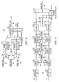
- FIG. 5 illustrates a block diagram of a telecommunication apparatus 60 in accordance with an embodiment of the present invention which generates sequential frames of data protected by nested hierarchical parity bits.
- User data is received on communication channel 62.
- Other types of data may be received as inputs on communication channels 64 and 66.
- Selectors (multiplexers) 68 and 70 select one of two inputs to feed via communication channels 72 and 74 to the active multilevel processor 76 and the standby multilevel processor 78, respectively.
- the labels "active" and “standby” refer to a given time of operation and that the roles of the multilevel processors can alternate between active and standby.
- the active label normally designates the multilevel processor which is actively receiving user data, processing the data and transmitting the user data on an output channel to interface circuit 82.
- the interface circuit receives clock inputs from clock 84 as does the active and standby processors.
- Interface circuit 82 selects whether to transmit output frames generated by the active or standby processors on output channel 88 to receiving equipment connected to output channel 88.
- Each of the processors 76 and 78 may comprise an apparatus such as shown in FIG. 1 which generates or builds frames based on input data. Assume active multilevel processor 76 is receiving user data from channel 62 via selector 68 and channel 72, while standby multilevel processor 78 receives other data from channel 66 by selector 70 and input channel 74. In this condition the processor 76 generates frames carrying the user data which are transmitted to interface circuit 82 which then couples the frames to output 88 for transmission to appropriate receiving apparatus. While this activity proceeds, standby multilevel processor 78 may receive test or maintenance data which is utilized to exercise or test the functions of the processor 78. Processor 78 generates output frames based on the test data and transmits these frames on output channel 81 to interface circuit 82.
- Interface circuit 82 selects between one of its inputs to process.
- input 80 is selected to be processed by interface circuit 82 and a resulting output transmitted on channel 88.
- Input on channel 81 representing the testing of processor 78 is not transmitted by the interface circuit to channel 88, but can be routed to other circuitry associated with such testing (not shown).
- user data 62 will be selected by both selectors 68 and 70 to provide concurrent inputs on channels 72 and 74 to both processor 76 and 78, respectively, prior to the desired time of transition.
- user data is routed to the standby processor 78 for a sufficient number of frames before the actual switch over is made to transmit data generated by standby processor 78.
- At least one frame of user data will have been forwarded to and processed by the standby processor 78 prior to the desired frame at which the transition is to occur.
- FIG. 6 illustrates a block diagram of an interface circuit 82 in accordance with an embodiment of the present invention.
- Registers 90 and 92 are associated with the active and standby processors 76 and 78, respectively, and receive frames generated from the processors on input channels 80 and 81.
- a first frame of data is generated by both of the processors and transmitted to interface circuit 82 on lines 80 and 81, respectively.
- Inversion circuits 94 and 96 process these frames stored in registers 90 and 92, respectively.
- the inversion circuits are used to selectively invert or change the polarity (state) of the lowest rank parity bit 26; the remainder of the frame is unchanged.
- a comparison circuit 98 compares parity bit 26 of the standby frame with the corresponding parity bit 26 of the corresponding active frame and provides control signals on output lines 100 to the inversion circuits. Comparison circuit 98 sends an output signal on line 100 to inversion circuit 96 to control whether parity bit 26 is to be inverted based upon whether it is equal to the corresponding parity bit in the active side of the same frame. Once this decision has been made, the comparison circuit 98 also transmits the comparison decision by path 101 to comparison circuit 106. In all succeeding frames the inversion circuit 96 will either invert or not invert the parity bit 26 based on the decision made during the current frame by comparison circuit 98.
- Inversion circuit 94 may have been inverting or not inverting the active side parity bit 26 prior to the first frame; the inversion choice of circuit 94 (the active side) remains unchanged during the active-to-standby changeover.
- Inversion circuits 102 and 104 receive the frames as processed by inversion circuits 94 and 96, respectively, and store predetermined parity inversion patterns (sequences) which are selected.
- the inversion circuits 102 and 104 invert or do not invert parity bit 38 depending upon the results of the comparison made by comparison circuit 106 and the prior inversion decision made by comparison circuit 98.
- the comparison circuit 106 determines whether the parity bit of the second rank (parity bit 38) of the standby frame is equal to the corresponding parity bit 38 in the corresponding active frame.
- the decisions by circuits 106 and 98 are transmitted on path 107 to comparison circuit 114.
- the output signals on control lines 108 from comparison circuit 106 are used to control inversion circuits 102 and 104.
- the inversion circuit 104 will receive and implement the inversion or non-inversion sequence as determined by the signal on line 108 from comparison circuit 106 during the current frame. This permits the state of the lower rank parity bit 26 previously determined by comparison circuit 98 and implemented by inversion circuit 96 to be used as part of the inversion determination of each bit in parity byte 38. The state of inversion or non-inversion of bits of the byte 38 by the active side circuit 102 is not changed. Circuits 102 and 104 do not change data in the processed frame except for the parity bits in the byte 38.
- Inversion circuits 110 and 112 receive the frames from circuits 102 and 104, respectively, and store predetermined sequences of inversions which are applied during the changeover from the active to standby apparatus.
- the inversion decision implemented by circuit 112 depends on whether comparison circuit 114 determines if the corresponding standby parity bit 58 is equal to the corresponding parity bit 58 in the active side during the same frame and on prior inversion decisions made by circuits 98 and 106. In accordance with the illustrative embodiment, this determination is implemented by control signals on output lines 116 from comparison circuit. This decision is made for each frame, but as explained above, will not vary once parity bit alignment is achieved. The state of inversion or non-inversion of active side bit 58 by circuit 110 is not changed.
- the frame output from inversion circuits 110 and 112 are received as inputs by shift registers 118 and 120 which each store a frame of data.
- the frame output on lines 122 and 124 from registers 118 and 120, respectively, provide inputs to comparator 126 which provides a bit-by-bit comparison of these frames.
- the true/false result of the complete frame comparison is provided on output line 128 and provides a means by which a determination is made that the standby side frame is in parity synchronization (alignment) with the active side frame, i.e. all parity bits in the standby side frame are equal to corresponding parity bits in the active side frame prior to making the transition.
- the frame output on lines 122 and 124 from the registers is also provided as inputs to selector 130 which selects either the active or standby frame of data to be coupled to the data output line 88 from interface circuit 82.
- a select control signal carried on line 132 determines which of the frames are selected.
- a system controller (not shown) receives the true/false signal from line 128 and is utilized to provide a control signal on select line 132 which prevents a transition from the active to the passive data stream until a true signal is received on line 128.
- a frame of data is processed by the standby processor 78 in parallel with the active processor 76 in order to enable the comparison circuits 98, 106, and 114 to make decisions as to whether the corresponding standby inversion circuits 96, 104, and 112 are to implement an appropriate inversion sequence of the parity bits 26, 38, and 58, respectively.
- the standby processor 78 In accordance with a preferred embodiment of the present invention, at least one frame is processed prior to the actual transition of transmitting frames processed by the standby processor 78.
- processor 76 is then the standby side and processor 78 is the active side.
- a subsequent active to standby transition causes the decisions made by comparison circuits 98, 106, 114 to result in corresponding inversion decisions to be implemented by the then standby inversion circuits 94, 102, and 110, respectively, while the decisions implemented by circuits 96, 104, and 112 remain unchanged.
- FIG. 7 illustrates a flow diagram in accordance with an exemplary embodiment of the present invention which illustrates steps which may be implemented by the apparatus shown in FIG. 6.
- a determination is made by step 152 of whether the lowest ranked parity bit in the standby side is equal to the corresponding parity bit in the active side, i.e. is B3 A -B3 S ? Where "B" represents a parity bit, "3" indicates rank, and the subscripts specify A(ctive) or S(tandby) association.
- the B3 parity bit inversion is first determined.
- a NO determination by step 152 results in the lowest ranked parity bit on the standby side (B3 S ) being inverted as indicated in step 154.
- the decision to invert or not invert the lowest parity bit is made during each frame.
- the notations B3, B2, and B1 correspond to the lowest, intermediate, and highest ranked parity bits 26, 38, and 58, as shown in FIGs. 2, 3, and 4. It will also be appreciated that the steps described for Fig. 7 are made on a bit by bit basis for each corresponding parity bit of the three parity bytes.
- a YES decision by determination step 152 leads to a further determination by determination step 156.
- a NO determination by step 156 results in step 158 causing an inversion decision for the parity bit 38 (B2 S ).
- This decision is stored and implemented, i.e. B2 S is to be inverted.
- a YES determination by step 156 results in a decision not to invert the second ranked parity bit.
- step 152 an inversion determination for the second ranked parity bit proceeds as follows.
- step 160 a determination is made in step 160 to apply an inversion sequence to the second order parity bit, wherein the sequence consists of inverting the second ranked parity bit during frames of even number. That is, during frame numbers 2, 4, 6,...., the second ranked parity bit 38 (B2 S (N)) is inverted; it is not inverted during odd numbered frames.
- a NO determination by step 162 results in step 164 implementing an inversion to be made of each second parity bit B2 S .
- step 164 the highest parity bit will be inverted in accordance with the sequence determined in step 166 where Bi S is inverted for frame numbers 3, 4, 7, 8, 11, 12, .... That is, inversions will be made in pairs of two with non-inversion being made in intermediate pairs of two. This indefinite sequence is continued in accordance with step 166.
- a YES determination by step 168 will result in the highest rank frame B1 S being inverted in accordance with a frame sequence of 2, 3, 6, 7, 10, 11,...., as indicated in step 168. If step 158 was executed, the highest ranked parity bit B1 S will be inverted in accordance with even numbered frames as indicated in step 170. That is, the highest order parity bit B1 S will be inverted during frames 2, 4, 6,....
- step 156 If the determination step 156 resulted in a YES determination, no preceding inversions of the third or second parity bits will have been initiated.
- a NO determination by step 172 results in the highest order parity bit B1 S being inverted in accordance with step 174.
- a YES determination by step 172 results in the termination of the alignment process at END 176.
- the inversion decisions made for B3 S , B2 S , and B1 S are made sequentially and implemented for all frames until the next active-to-standby transition.
- steps 160, 166, 168, and 170 involve the implementation of a predetermined bit inversion sequence based on the frame number (position) relative to a first beginning frame. It is believed to be apparent to those skilled in the art that such repeating sequences can be implemented in various ways including state machines, logic circuits, and software processes. In accordance with the preferred embodiment of the present invention, in order to enhance the processing speed, it is preferred that inversion decisions and bit inversions be implemented in hardware. It is believed to be apparent to those skilled in the art that this exemplary technique explained with regard to three levels of priority can be utilized to handle various levels of nested parity bits including parity ranks of 2, 3, and greater than 3.
- predetermined inversion sequences of the parity bits are utilized depending upon the comparisons of the standby-to-active parity bits and depending upon the prior history of inversion decisions made with regard to lower ranked parity bits. This section provides an explanation of why the particular inversion patterns defined in steps 160, 166, 168, and 170 are used to achieve parity bit alignment.
- frame 1 corresponds to the first frame in which the active and standby apparatus are processing equivalent data.
- the parity inserted in frame 1 by the active and standby sides may be different since the two sides were processing different data prior to frame 1.
- B3(N+1) is the B3 parity bit 26 inserted in frame N+1, where D3(N) includes all of the corresponding payload 22 and header 24 data bits in subframe 20 of frame N in FIG. 2, except the B3 parity bit, which may be different between the active and standby sides and is shown separately as B3(N).
- B2(N+1) is the B2 parity bit 38 inserted in frame N+1, where D2(N) includes all of the corresponding payload 22 and header data bits 24 and 26 in subframe 34 of frame N in FIG.
- B1(N+1) is the B1 parity bit 58 inserted in frame N+1, where D1(N) includes all of the corresponding payload 22 and header data bits 24, 36, and 56 in subframe 54 of frame N in FIG. 2, except the B3, B2, and B1 parity bits 26, 38, and 58, which may be different between the active and standby sides and are shown separately as B3(N), B2(N), and B1(N), respectively.
- parity and data corresponding to the active and standby sides are designated by the subscripts A and S, respectively (e.g. B3 A ,B3 S ).
- B 3 ( N ⁇ 1 ) D 3 ( N ⁇ 2 ) + B 3 ( N ⁇ 2 )
- B 3 ( N ) D 3 ( N ⁇ 1 ) + B 3 ( N ⁇ 1 )
- B 3 ( N + 1 ) D 3 ( N ) + B 3 ( N )
- B3 A (1) B3 S (1)
- B3 A (1) B3 S (1)
- B3 S (1) B3 S (1)
- B3 S and B3 A parity bits will be equal in all subsequent frames.
- B3 A (1) ⁇ B3 S (1) B3 S will be the inverse of B3 A in all subsequent frames.
- B3 S can be made equal to B3 A by comparing their values in corresponding frames and if not equal introducing an inversion in the parity for the standby side as shown in FIG. 7.
- B 2 ( N ⁇ 1 ) D 2 ( N ⁇ 2 ) + B 3 ( N ⁇ 2 ) + B 2 ( N ⁇ 2 )
- B 2 ( N ) D 2 ( N ⁇ 1 ) + B 3 ( N ⁇ 1 ) + B 2 ( N ⁇ 1 )
- B 2 ( N + 1 ) D 2 ( N ) + B 3 ( N ) + B 2 ( N )
- B 2 ( N + 1 ) [ D 2 ( N ) + D 2 ( N ⁇ 1 ) + ... + D 2 ( 1 ) ] + [ B 3 ( N ) + B 3 ( N ⁇ 1 ) + ... + B 3 ( 1 ) ] + B 2 ( 1 )
- B3 A (1) B3 S (1)
- B2 A (1) B2 S (1)
- the B2 S and B2 A parity bits will be equal in all subsequent frames.
- B2 A (1) ⁇ B2 S (1) B2 S will be the inverse of B2 A in all subsequent frames.
- This relationship taken together with the previous relationship for N even shows that the relationship between B2 S and B2 A for B3 A ⁇ B3 S is the opposite for odd and even frames. This difference can be accounted for by inverting B2 S in every other frame as shown in FIG. 7, after which B2 S will either equal B2 A or its inverse in every frame.
- B 1 A ( N + 1 ) D 1 ( N ) + B 3 A ( N ) + B 2 A ( N ) + B 1 A ( N )
- B 1 S ( N + 1 ) D 1 ( N ) + B 3 S ( N ) + B 2 S ( N ) + B 1 S ( N )
- B 1 ( N ⁇ 1 ) D 1 ( N ⁇ 2 ) + B 3 ( N ⁇ 2 ) + B 2 ( N ⁇ 2 ) + B 1 ( N ⁇ 2 )
- B 1 ( N ) D 1 ( N ⁇ 1 ) + B 3 ( N ⁇ 1 ) + B 2 ( N ⁇ 1 ) + B 1 ( N ⁇ 1 )
- B 1 ( N + 1 ) D 1 ( N ) + B 3 ( N ⁇ 1 ) + B 2 ( N ⁇ 1 ) + B 1 ( N ⁇ 1 )
- B 1 ( N + 1 ) D 1 ( N ) + B 3 ( N ⁇ 1 ) + B 2 ( N
- B1 S and B1 A as determined for Cases 1-4 can be accounted for by introducing the appropriate inversions in B1 S as shown in FIG. 7.
Landscapes
- Engineering & Computer Science (AREA)
- Theoretical Computer Science (AREA)
- Computer Networks & Wireless Communication (AREA)
- Signal Processing (AREA)
- Quality & Reliability (AREA)
- Physics & Mathematics (AREA)
- General Engineering & Computer Science (AREA)
- General Physics & Mathematics (AREA)
- Detection And Prevention Of Errors In Transmission (AREA)
- Detection And Correction Of Errors (AREA)
- Error Detection And Correction (AREA)
- Time-Division Multiplex Systems (AREA)
Claims (10)
- Verfahren zur Synchronisation der Paritätsbits während einer Änderung der Verarbeitung von Rahmen von Daten in einer Telekommunikationsvorrichtung von einer ersten Vorrichtung (76) zu einer zweiten Vorrichtung (78), wobei die erste Vorrichtung (76) aufeinanderfolgende Rahmen von Daten in einer aktiven Betriebsart verarbeitet und die zweite Vorrichtung (78) in einer Bereitschafts-Betriebsart tätig ist, in der sie bereit ist, die Verarbeitung der Rahmen von Daten von der ersten Vorrichtung zu übernehmen, wobei jeder der aufeinanderfolgenden Rahmen von Daten mehrere hierarchisch erzeugte Paritätsbits enthält,
GEKENNZEICHNET DURCHa) Bestimmen (152), ob das niedrigstrangige Paritätsbit in einem ersten Rahmen von Daten, der durch die zweite Vorrichtung (78) verarbeitet wird, die gleiche Polarität wie das niedrigstrangige Paritätsbit aufweist, das während des ersten Rahmens durch die erste Vorrichtung (76) verarbeitet wurde;b) Umkehren (154) der Polarität des niedrigstrangigen Paritätsbits im ersten Rahmen von Daten, der durch die zweite Vorrichtung (78) verarbeitet wird, wenn seine Polarität nicht die gleiche wie die Polarität des entsprechenden Paritätsbits ist, das während des ersten Rahmens durch die erste Vorrichtung (76) verarbeitet wurde;c) Bestimmen (156, 162, 172), für Paritätsbits, die durch die zweite Vorrichtung (76) verarbeitet werden, für jedes Paritätsbit von höherem Rang als dem niedrigstrangigen Paritätsbit, ob eine Polaritätsumkehr eines niedrigerrangigen Paritätsbits aufgetreten ist;d) bei Zutreffen der Bestimmung von Schritt c) für eines der höherrangigen Paritätsbits, Auswählen einer Umkehrabfolge aus einem vorbestimmten Satz von Umkehrabfolgen (158, 170; 160, 168; 160, 164, 166), um Umkehrungen der Parität des einen Paritätsbits in Rahmen von Daten, die durch die zweite Vorrichtung im Anschluss an den ersten Rahmen verarbeitet werden, zu steuern, wobei die Auswahl der einen Umkehrabfolge auf der Anzahl der Umkehrungen von niedrigerrangigen Paritätsbits beruht. - Verfahren nach Anspruch 1, wobei Schritt d) ferner den Schritt der Auswahl der einen Umkehrabfolge auch auf basierend darauf umfasst, ob die Polarität des einen Paritätsbits von höherem Rang, das durch die zweite Vorrichtung (78) verarbeitet wird, nicht die gleiche wie die Polarität des entsprechenden Paritätsbits ist, das durch die erste Vorrichtung (76) verarbeitet wurde.
- Verfahren nach Anspruch 1, ferner umfassend einen auf Schritt d) von Anspruch 1 folgenden Schritt des Bestimmens (172), ob das höchstrangige Paritätsbit in einem Rahmen von Daten, der durch die zweite Vorrichtung verarbeitet wird, die gleiche Polarität wie das höchstrangige Paritätsbit aufweist, das während des entsprechenden Rahmens durch die erste Vorrichtung (76) verarbeitet wurde, und Umkehren (174) der Polarität des höchstrangigen Paritätsbits im Rahmen von Daten, der durch die zweite Vorrichtung (78) verarbeitet wird, wenn seine Polarität nicht die gleiche wie die Polarität des entsprechenden Paritätsbits ist, das während des entsprechenden Rahmens durch die erste Vorrichtung verarbeitet wurde.
- Verfahren nach Anspruch 1, wobei der Auswahlschritt nach Schritt d) von Anspruch 1 während des ersten Rahmens von Daten vorgenommen wird.
- Verfahren nach Anspruch 1, ferner umfassend den Schritt des Bereitstellens von aufeinanderfolgenden Rahmen von Daten im Anschluss an den ersten Rahmen von Daten und des Synchronisierens der Paritätsbits in den Daten für jeden Rahmen durch die zweite Vorrichtung.
- Verfahren nach Anspruch 1, wobei die erste und die zweite Vorrichtung synchron formatierte Daten verarbeiten.
- Verfahren nach Anspruch 1, ferner umfassend den Schritt des Beginnens mit der Verarbeitung der Rahmen von Daten durch die zweite Vorrichtung mit dem ersten Rahmen von Daten, und wobei die zweite Vorrichtung über keinen Zugriff auf die vorherige Geschichte des Zustands der Paritätsbits für Daten verfügt, die vorher durch die erste Vorrichtung verarbeitet wurden.
- Verfahren nach Anspruch 1, ferner umfassend die Schritte des Erzeugens von ersten und zweiten Datenströmen der Rahmen von Daten durch die erste bzw. die zweite Vorrichtung, des Auswählens eines Ausgangsdatenstroms aus dem ersten und dem zweiten Datenstrom, und des Auswählens des zweiten Datenstroms als den Ausgangsdatenstrom nur nachdem alle gereihten Paritätsbits in Rahmen von Daten im zweiten Datenstrom synchronisiert wurden, damit sie die gleichen wie entsprechende Paritätsbits in Rahmen von Daten im ersten Datenstrom sind.
- Telekommunikationsvorrichtung, die eine erste und eine zweite Verarbeitungsvorrichtung (76, 78) aufweist, wobei die erste Vorrichtung (76) aufeinanderfolgende Rahmen von Daten in einer aktiven Betriebsart verarbeitet und die zweite Vorrichtung (78) in einer Bereitschafts-Betriebsart tätig ist, in der sie bereit ist, die Verarbeitung der Rahmen von Daten von der ersten Vorrichtung zu übernehmen, wobei jeder der aufeinanderfolgenden Rahmen von Daten mehrere hierarchisch erzeugte Paritätsbits enthält, GEKENNZEICHNET DURCH ein Mittel, um die Paritätsbits während einer Änderung der Verarbeitung von Rahmen von Daten von der ersten Vorrichtung zur zweiten Vorrichtung zu synchronisieren, umfassend:a) ein erstes Mittel (98), um zu bestimmen, ob das niedrigstrangige Paritätsbit in einem ersten Rahmen von Daten, der durch die zweite Vorrichtung verarbeitet wird, die gleiche Polarität wie das niedrigstrangige Paritätsbit aufweist, das während des ersten Rahmens durch die erste Vorrichtung verarbeitet wurde;b) ein Mittel (94, 96), das auf dieses erste Mittel (98) anspricht, um die Polarität des niedrigstrangigen Paritätsbits im ersten Rahmen von Daten, der durch die zweite Vorrichtung verarbeitet wird, umzukehren, wenn seine Polarität nicht die gleiche wie die Polarität des entsprechenden Paritätsbits ist, das während des ersten Rahmens durch die erste Vorrichtung verarbeitet wurde;c) ein zweites Mittel (106), um für jedes Paritätsbit von höherem Rang als dem niedrigstrangigen Paritätsbit zu bestimmen, ob eine Polaritätsumkehr eines niedrigerrangigen Paritätsbits aufgetreten ist;d) ein Mittel (102, 104), um eine Umkehrabfolge aus einem vorbestimmten Satz von Umkehrabfolgen auszuwählen, um Umkehrungen der Parität eines der höherrangigen Paritätsbits in Rahmen von Daten, die durch die zweite Vorrichtung im Anschluss an den ersten Rahmen verarbeitet werden, zu steuern, wenn die Bestimmung des zweiten Mittels für dieses eine der höherrangigen Paritätsbits zutrifft, wobei das Auswahlmittel die Auswahl auf Basis der Anzahl der Umkehrungen von niedrigerrangigen Paritätsbits vornimmt.
- Vorrichtung nach Anspruch 9, wobei das Auswahlmittel ferner dazu geeignet ist, die eine Umkehrabfolge auf Basis darauf auszuwählen, ob die Polarität des einen Paritätsbits der höherrangigen Paritätsbits, das durch die zweite Vorrichtung verarbeitet wird, nicht die gleiche wie die Polarität des entsprechenden Paritätsbits ist, das durch die erste Vorrichtung verarbeitet wurde.
Applications Claiming Priority (2)
| Application Number | Priority Date | Filing Date | Title |
|---|---|---|---|
| US08/430,627 US5838698A (en) | 1995-04-28 | 1995-04-28 | Alignment of parity bits to eliminate errors in switching from an active to a standby processing circuit |
| US430627 | 1995-04-28 |
Publications (3)
| Publication Number | Publication Date |
|---|---|
| EP0740435A2 EP0740435A2 (de) | 1996-10-30 |
| EP0740435A3 EP0740435A3 (de) | 2000-02-23 |
| EP0740435B1 true EP0740435B1 (de) | 2006-10-11 |
Family
ID=23708364
Family Applications (1)
| Application Number | Title | Priority Date | Filing Date |
|---|---|---|---|
| EP96302686A Expired - Lifetime EP0740435B1 (de) | 1995-04-28 | 1996-04-17 | Synchronisation von Paritätsbits zur Fehlervermeidung beim Umschalten zwischen einem aktiven und einem stand-by Prozessor |
Country Status (6)
| Country | Link |
|---|---|
| US (1) | US5838698A (de) |
| EP (1) | EP0740435B1 (de) |
| JP (1) | JP3263307B2 (de) |
| CA (1) | CA2171225C (de) |
| DE (1) | DE69636613T2 (de) |
| ES (1) | ES2271949T3 (de) |
Families Citing this family (8)
| Publication number | Priority date | Publication date | Assignee | Title |
|---|---|---|---|---|
| KR100233458B1 (ko) * | 1997-05-19 | 1999-12-01 | 윤종용 | 원격 다중 가입자의 호처리 이중화 방법 |
| US6738935B1 (en) * | 2000-02-07 | 2004-05-18 | 3Com Corporation | Coding sublayer for multi-channel media with error correction |
| AU2002326417A1 (en) * | 2001-07-20 | 2003-03-03 | Hill-Rom Services, Inc. | Badge for a locating and tracking system |
| US7385929B1 (en) * | 2001-09-25 | 2008-06-10 | Atheros Communications, Inc. | Method and system for detecting false packets in wireless communications systems |
| WO2010076835A1 (en) | 2008-12-31 | 2010-07-08 | Christophe Laurent | Error correction code for unidirectional memory |
| JP5649855B2 (ja) * | 2010-06-01 | 2015-01-07 | 富士通株式会社 | 伝送装置およびパリティ演算方法 |
| US10734110B2 (en) | 2018-12-05 | 2020-08-04 | Hill-Rom Services, Inc. | Caregiver locating tag having advanced functionality |
| US11411584B2 (en) * | 2020-09-28 | 2022-08-09 | Western Digital Technologies, Inc. | Data storage device channel encoding current data using redundancy bits generated over preceding data |
Family Cites Families (6)
| Publication number | Priority date | Publication date | Assignee | Title |
|---|---|---|---|---|
| US4546475A (en) * | 1982-12-06 | 1985-10-08 | At&T Bell Laboratories | Parity checking arrangement |
| US4543651A (en) * | 1983-09-12 | 1985-09-24 | At&T Bell Laboratories | Duplicated time division switching system |
| JPH03198544A (ja) * | 1989-12-27 | 1991-08-29 | Nec Corp | パリティ計数回路 |
| US5392424A (en) * | 1992-06-11 | 1995-02-21 | Allen-Bradley Company, Inc. | Apparatus for detecting parity errors among asynchronous digital signals |
| DE4226599C2 (de) * | 1992-08-11 | 1994-08-04 | Siemens Ag | Verfahren zur Fehlererkennung in digitalen Kommunikationssystemen |
| FI96078C (fi) * | 1994-05-09 | 1996-04-25 | Nokia Telecommunications Oy | Menetelmä yksikönvaihdon suorittamiseksi pakettimuotoista dataa välittävässä tietoliikennesolmussa |
-
1995
- 1995-04-28 US US08/430,627 patent/US5838698A/en not_active Expired - Fee Related
-
1996
- 1996-03-07 CA CA002171225A patent/CA2171225C/en not_active Expired - Fee Related
- 1996-04-17 DE DE69636613T patent/DE69636613T2/de not_active Expired - Fee Related
- 1996-04-17 EP EP96302686A patent/EP0740435B1/de not_active Expired - Lifetime
- 1996-04-17 ES ES96302686T patent/ES2271949T3/es not_active Expired - Lifetime
- 1996-04-26 JP JP10658296A patent/JP3263307B2/ja not_active Expired - Fee Related
Also Published As
| Publication number | Publication date |
|---|---|
| US5838698A (en) | 1998-11-17 |
| EP0740435A3 (de) | 2000-02-23 |
| CA2171225A1 (en) | 1996-10-29 |
| DE69636613D1 (de) | 2006-11-23 |
| ES2271949T3 (es) | 2007-04-16 |
| JP3263307B2 (ja) | 2002-03-04 |
| EP0740435A2 (de) | 1996-10-30 |
| CA2171225C (en) | 1999-12-28 |
| JPH0983497A (ja) | 1997-03-28 |
| DE69636613T2 (de) | 2007-08-09 |
Similar Documents
| Publication | Publication Date | Title |
|---|---|---|
| US6212660B1 (en) | Methods and apparatuses for identification of the position of data packets which are located in a serial received data stream | |
| US4712215A (en) | CRC calculation machine for separate calculation of checkbits for the header packet and data packet | |
| EP0443754A2 (de) | Verfahren und Gerät zur Wahrnehmung eines Rahmenausrichtungswortes in einem Datenstrom | |
| EP0310110A2 (de) | (1+N)störungsfreies Kanalumschaltungssystem | |
| US7287176B2 (en) | Apparatus, method and storage medium for carrying out deskew among multiple lanes for use in division transmission of large-capacity data | |
| EP0419805A2 (de) | Parallele Architektur zur schnellen Flag-Erkennung und Paketidentifizierung | |
| EP0740435B1 (de) | Synchronisation von Paritätsbits zur Fehlervermeidung beim Umschalten zwischen einem aktiven und einem stand-by Prozessor | |
| EP0371593B1 (de) | Verfahren zur Initialisierung oder Synchronisierung einer Übertragungsleitung | |
| US4567595A (en) | Multiline error detection circuit | |
| JPH01206750A (ja) | ブロック同期方式 | |
| JP3263671B2 (ja) | 誤り検出装置 | |
| US4837848A (en) | Apparatus for selecting a reference line for image data compression | |
| JPH01302946A (ja) | コード・バイオレーション検出回路 | |
| JPS63274248A (ja) | 伝送エラ−検出部の診断方法 | |
| JPS61283241A (ja) | デ−タ通信受信装置 | |
| JP2774318B2 (ja) | 伝送制御信号検出装置およびその制御方法 | |
| JP2624210B2 (ja) | 装置内監視回路 | |
| EP1480370A1 (de) | Übertragungsdatenrahmensynchronisationsverfahren und übertragungsdatenrahmensynchronisationsschaltung | |
| JP2573560B2 (ja) | フレ−ム同期方式 | |
| JPS58162152A (ja) | ル−プ伝送方式 | |
| JPH1084334A (ja) | データ伝送方式 | |
| JPS60219852A (ja) | コ−ド処理方式 | |
| JPH0964848A (ja) | 巡回冗長符号誤り検査方式 | |
| JPH01185040A (ja) | 情報伝送方法および伝送装置 | |
| JPH06303246A (ja) | 障害個所検索方式 |
Legal Events
| Date | Code | Title | Description |
|---|---|---|---|
| PUAI | Public reference made under article 153(3) epc to a published international application that has entered the european phase |
Free format text: ORIGINAL CODE: 0009012 |
|
| AK | Designated contracting states |
Kind code of ref document: A2 Designated state(s): DE ES FR GB IT |
|
| PUAL | Search report despatched |
Free format text: ORIGINAL CODE: 0009013 |
|
| AK | Designated contracting states |
Kind code of ref document: A3 Designated state(s): DE ES FR GB IT |
|
| 17P | Request for examination filed |
Effective date: 20000811 |
|
| GRAP | Despatch of communication of intention to grant a patent |
Free format text: ORIGINAL CODE: EPIDOSNIGR1 |
|
| GRAS | Grant fee paid |
Free format text: ORIGINAL CODE: EPIDOSNIGR3 |
|
| GRAA | (expected) grant |
Free format text: ORIGINAL CODE: 0009210 |
|
| AK | Designated contracting states |
Kind code of ref document: B1 Designated state(s): DE ES FR GB IT |
|
| PG25 | Lapsed in a contracting state [announced via postgrant information from national office to epo] |
Ref country code: IT Free format text: LAPSE BECAUSE OF FAILURE TO SUBMIT A TRANSLATION OF THE DESCRIPTION OR TO PAY THE FEE WITHIN THE PRE;WARNING: LAPSES OF ITALIAN PATENTS WITH EFFECTIVE DATE BEFORE 2007 MAY HAVE OCCURRED AT ANY TIME BEFORE 2007. THE CORRECT EFFECTIVE DATE MAY BE DIFFERENT FROM THE ONE RECORDED.SCRIBED TIME-LIMIT Effective date: 20061011 |
|
| REG | Reference to a national code |
Ref country code: GB Ref legal event code: FG4D |
|
| REF | Corresponds to: |
Ref document number: 69636613 Country of ref document: DE Date of ref document: 20061123 Kind code of ref document: P |
|
| REG | Reference to a national code |
Ref country code: ES Ref legal event code: FG2A Ref document number: 2271949 Country of ref document: ES Kind code of ref document: T3 |
|
| ET | Fr: translation filed | ||
| PLBE | No opposition filed within time limit |
Free format text: ORIGINAL CODE: 0009261 |
|
| STAA | Information on the status of an ep patent application or granted ep patent |
Free format text: STATUS: NO OPPOSITION FILED WITHIN TIME LIMIT |
|
| 26N | No opposition filed |
Effective date: 20070712 |
|
| PGFP | Annual fee paid to national office [announced via postgrant information from national office to epo] |
Ref country code: ES Payment date: 20080429 Year of fee payment: 13 Ref country code: DE Payment date: 20080418 Year of fee payment: 13 |
|
| PGFP | Annual fee paid to national office [announced via postgrant information from national office to epo] |
Ref country code: FR Payment date: 20080412 Year of fee payment: 13 |
|
| PGFP | Annual fee paid to national office [announced via postgrant information from national office to epo] |
Ref country code: GB Payment date: 20080421 Year of fee payment: 13 |
|
| GBPC | Gb: european patent ceased through non-payment of renewal fee |
Effective date: 20090417 |
|
| REG | Reference to a national code |
Ref country code: FR Ref legal event code: ST Effective date: 20091231 |
|
| PG25 | Lapsed in a contracting state [announced via postgrant information from national office to epo] |
Ref country code: DE Free format text: LAPSE BECAUSE OF NON-PAYMENT OF DUE FEES Effective date: 20091103 |
|
| PG25 | Lapsed in a contracting state [announced via postgrant information from national office to epo] |
Ref country code: GB Free format text: LAPSE BECAUSE OF NON-PAYMENT OF DUE FEES Effective date: 20090417 Ref country code: FR Free format text: LAPSE BECAUSE OF NON-PAYMENT OF DUE FEES Effective date: 20091222 |
|
| REG | Reference to a national code |
Ref country code: ES Ref legal event code: FD2A Effective date: 20090418 |
|
| PG25 | Lapsed in a contracting state [announced via postgrant information from national office to epo] |
Ref country code: ES Free format text: LAPSE BECAUSE OF NON-PAYMENT OF DUE FEES Effective date: 20090418 |