EP0745975A2 - System und Verfahren zur gleichzeitigen Nachprüfung von optischen Aufzeichnung von Daten und dazu verwendbares optisches Datenaufzeichnungsmedium - Google Patents
System und Verfahren zur gleichzeitigen Nachprüfung von optischen Aufzeichnung von Daten und dazu verwendbares optisches Datenaufzeichnungsmedium Download PDFInfo
- Publication number
- EP0745975A2 EP0745975A2 EP96303859A EP96303859A EP0745975A2 EP 0745975 A2 EP0745975 A2 EP 0745975A2 EP 96303859 A EP96303859 A EP 96303859A EP 96303859 A EP96303859 A EP 96303859A EP 0745975 A2 EP0745975 A2 EP 0745975A2
- Authority
- EP
- European Patent Office
- Prior art keywords
- writing
- film
- data writing
- light
- state
- Prior art date
- Legal status (The legal status is an assumption and is not a legal conclusion. Google has not performed a legal analysis and makes no representation as to the accuracy of the status listed.)
- Granted
Links
Images


Classifications
-
- G—PHYSICS
- G11—INFORMATION STORAGE
- G11B—INFORMATION STORAGE BASED ON RELATIVE MOVEMENT BETWEEN RECORD CARRIER AND TRANSDUCER
- G11B7/00—Recording or reproducing by optical means, e.g. recording using a thermal beam of optical radiation by modifying optical properties or the physical structure, reproducing using an optical beam at lower power by sensing optical properties; Record carriers therefor
- G11B7/24—Record carriers characterised by shape, structure or physical properties, or by the selection of the material
- G11B7/241—Record carriers characterised by shape, structure or physical properties, or by the selection of the material characterised by the selection of the material
- G11B7/252—Record carriers characterised by shape, structure or physical properties, or by the selection of the material characterised by the selection of the material of layers other than recording layers
- G11B7/258—Record carriers characterised by shape, structure or physical properties, or by the selection of the material characterised by the selection of the material of layers other than recording layers of reflective layers
-
- G—PHYSICS
- G11—INFORMATION STORAGE
- G11B—INFORMATION STORAGE BASED ON RELATIVE MOVEMENT BETWEEN RECORD CARRIER AND TRANSDUCER
- G11B7/00—Recording or reproducing by optical means, e.g. recording using a thermal beam of optical radiation by modifying optical properties or the physical structure, reproducing using an optical beam at lower power by sensing optical properties; Record carriers therefor
- G11B7/08—Disposition or mounting of heads or light sources relatively to record carriers
-
- G—PHYSICS
- G11—INFORMATION STORAGE
- G11B—INFORMATION STORAGE BASED ON RELATIVE MOVEMENT BETWEEN RECORD CARRIER AND TRANSDUCER
- G11B7/00—Recording or reproducing by optical means, e.g. recording using a thermal beam of optical radiation by modifying optical properties or the physical structure, reproducing using an optical beam at lower power by sensing optical properties; Record carriers therefor
- G11B7/004—Recording, reproducing or erasing methods; Read, write or erase circuits therefor
- G11B7/0045—Recording
-
- G—PHYSICS
- G11—INFORMATION STORAGE
- G11B—INFORMATION STORAGE BASED ON RELATIVE MOVEMENT BETWEEN RECORD CARRIER AND TRANSDUCER
- G11B7/00—Recording or reproducing by optical means, e.g. recording using a thermal beam of optical radiation by modifying optical properties or the physical structure, reproducing using an optical beam at lower power by sensing optical properties; Record carriers therefor
- G11B7/004—Recording, reproducing or erasing methods; Read, write or erase circuits therefor
- G11B7/0045—Recording
- G11B7/00454—Recording involving phase-change effects
-
- G—PHYSICS
- G11—INFORMATION STORAGE
- G11B—INFORMATION STORAGE BASED ON RELATIVE MOVEMENT BETWEEN RECORD CARRIER AND TRANSDUCER
- G11B7/00—Recording or reproducing by optical means, e.g. recording using a thermal beam of optical radiation by modifying optical properties or the physical structure, reproducing using an optical beam at lower power by sensing optical properties; Record carriers therefor
- G11B7/004—Recording, reproducing or erasing methods; Read, write or erase circuits therefor
- G11B7/0045—Recording
- G11B7/00458—Verification, i.e. checking data during or after recording
-
- G—PHYSICS
- G11—INFORMATION STORAGE
- G11B—INFORMATION STORAGE BASED ON RELATIVE MOVEMENT BETWEEN RECORD CARRIER AND TRANSDUCER
- G11B7/00—Recording or reproducing by optical means, e.g. recording using a thermal beam of optical radiation by modifying optical properties or the physical structure, reproducing using an optical beam at lower power by sensing optical properties; Record carriers therefor
- G11B7/004—Recording, reproducing or erasing methods; Read, write or erase circuits therefor
- G11B7/005—Reproducing
-
- G—PHYSICS
- G11—INFORMATION STORAGE
- G11B—INFORMATION STORAGE BASED ON RELATIVE MOVEMENT BETWEEN RECORD CARRIER AND TRANSDUCER
- G11B7/00—Recording or reproducing by optical means, e.g. recording using a thermal beam of optical radiation by modifying optical properties or the physical structure, reproducing using an optical beam at lower power by sensing optical properties; Record carriers therefor
- G11B7/004—Recording, reproducing or erasing methods; Read, write or erase circuits therefor
- G11B7/0055—Erasing
- G11B7/00557—Erasing involving phase-change media
-
- G—PHYSICS
- G11—INFORMATION STORAGE
- G11B—INFORMATION STORAGE BASED ON RELATIVE MOVEMENT BETWEEN RECORD CARRIER AND TRANSDUCER
- G11B7/00—Recording or reproducing by optical means, e.g. recording using a thermal beam of optical radiation by modifying optical properties or the physical structure, reproducing using an optical beam at lower power by sensing optical properties; Record carriers therefor
- G11B7/24—Record carriers characterised by shape, structure or physical properties, or by the selection of the material
-
- G—PHYSICS
- G11—INFORMATION STORAGE
- G11B—INFORMATION STORAGE BASED ON RELATIVE MOVEMENT BETWEEN RECORD CARRIER AND TRANSDUCER
- G11B7/00—Recording or reproducing by optical means, e.g. recording using a thermal beam of optical radiation by modifying optical properties or the physical structure, reproducing using an optical beam at lower power by sensing optical properties; Record carriers therefor
- G11B7/24—Record carriers characterised by shape, structure or physical properties, or by the selection of the material
- G11B7/241—Record carriers characterised by shape, structure or physical properties, or by the selection of the material characterised by the selection of the material
- G11B7/242—Record carriers characterised by shape, structure or physical properties, or by the selection of the material characterised by the selection of the material of recording layers
- G11B7/243—Record carriers characterised by shape, structure or physical properties, or by the selection of the material characterised by the selection of the material of recording layers comprising inorganic materials only, e.g. ablative layers
-
- G—PHYSICS
- G11—INFORMATION STORAGE
- G11B—INFORMATION STORAGE BASED ON RELATIVE MOVEMENT BETWEEN RECORD CARRIER AND TRANSDUCER
- G11B7/00—Recording or reproducing by optical means, e.g. recording using a thermal beam of optical radiation by modifying optical properties or the physical structure, reproducing using an optical beam at lower power by sensing optical properties; Record carriers therefor
- G11B7/24—Record carriers characterised by shape, structure or physical properties, or by the selection of the material
- G11B7/241—Record carriers characterised by shape, structure or physical properties, or by the selection of the material characterised by the selection of the material
- G11B7/242—Record carriers characterised by shape, structure or physical properties, or by the selection of the material characterised by the selection of the material of recording layers
- G11B7/243—Record carriers characterised by shape, structure or physical properties, or by the selection of the material characterised by the selection of the material of recording layers comprising inorganic materials only, e.g. ablative layers
- G11B2007/24302—Metals or metalloids
- G11B2007/24312—Metals or metalloids group 14 elements (e.g. Si, Ge, Sn)
-
- G—PHYSICS
- G11—INFORMATION STORAGE
- G11B—INFORMATION STORAGE BASED ON RELATIVE MOVEMENT BETWEEN RECORD CARRIER AND TRANSDUCER
- G11B7/00—Recording or reproducing by optical means, e.g. recording using a thermal beam of optical radiation by modifying optical properties or the physical structure, reproducing using an optical beam at lower power by sensing optical properties; Record carriers therefor
- G11B7/24—Record carriers characterised by shape, structure or physical properties, or by the selection of the material
- G11B7/241—Record carriers characterised by shape, structure or physical properties, or by the selection of the material characterised by the selection of the material
- G11B7/242—Record carriers characterised by shape, structure or physical properties, or by the selection of the material characterised by the selection of the material of recording layers
- G11B7/243—Record carriers characterised by shape, structure or physical properties, or by the selection of the material characterised by the selection of the material of recording layers comprising inorganic materials only, e.g. ablative layers
- G11B2007/24302—Metals or metalloids
- G11B2007/24314—Metals or metalloids group 15 elements (e.g. Sb, Bi)
-
- G—PHYSICS
- G11—INFORMATION STORAGE
- G11B—INFORMATION STORAGE BASED ON RELATIVE MOVEMENT BETWEEN RECORD CARRIER AND TRANSDUCER
- G11B7/00—Recording or reproducing by optical means, e.g. recording using a thermal beam of optical radiation by modifying optical properties or the physical structure, reproducing using an optical beam at lower power by sensing optical properties; Record carriers therefor
- G11B7/24—Record carriers characterised by shape, structure or physical properties, or by the selection of the material
- G11B7/241—Record carriers characterised by shape, structure or physical properties, or by the selection of the material characterised by the selection of the material
- G11B7/242—Record carriers characterised by shape, structure or physical properties, or by the selection of the material characterised by the selection of the material of recording layers
- G11B7/243—Record carriers characterised by shape, structure or physical properties, or by the selection of the material characterised by the selection of the material of recording layers comprising inorganic materials only, e.g. ablative layers
- G11B2007/24302—Metals or metalloids
- G11B2007/24316—Metals or metalloids group 16 elements (i.e. chalcogenides, Se, Te)
-
- G—PHYSICS
- G11—INFORMATION STORAGE
- G11B—INFORMATION STORAGE BASED ON RELATIVE MOVEMENT BETWEEN RECORD CARRIER AND TRANSDUCER
- G11B7/00—Recording or reproducing by optical means, e.g. recording using a thermal beam of optical radiation by modifying optical properties or the physical structure, reproducing using an optical beam at lower power by sensing optical properties; Record carriers therefor
- G11B7/24—Record carriers characterised by shape, structure or physical properties, or by the selection of the material
- G11B7/241—Record carriers characterised by shape, structure or physical properties, or by the selection of the material characterised by the selection of the material
- G11B7/252—Record carriers characterised by shape, structure or physical properties, or by the selection of the material characterised by the selection of the material of layers other than recording layers
- G11B7/253—Record carriers characterised by shape, structure or physical properties, or by the selection of the material characterised by the selection of the material of layers other than recording layers of substrates
- G11B7/2533—Record carriers characterised by shape, structure or physical properties, or by the selection of the material characterised by the selection of the material of layers other than recording layers of substrates comprising resins
- G11B7/2534—Record carriers characterised by shape, structure or physical properties, or by the selection of the material characterised by the selection of the material of layers other than recording layers of substrates comprising resins polycarbonates [PC]
-
- G—PHYSICS
- G11—INFORMATION STORAGE
- G11B—INFORMATION STORAGE BASED ON RELATIVE MOVEMENT BETWEEN RECORD CARRIER AND TRANSDUCER
- G11B7/00—Recording or reproducing by optical means, e.g. recording using a thermal beam of optical radiation by modifying optical properties or the physical structure, reproducing using an optical beam at lower power by sensing optical properties; Record carriers therefor
- G11B7/24—Record carriers characterised by shape, structure or physical properties, or by the selection of the material
- G11B7/241—Record carriers characterised by shape, structure or physical properties, or by the selection of the material characterised by the selection of the material
- G11B7/252—Record carriers characterised by shape, structure or physical properties, or by the selection of the material characterised by the selection of the material of layers other than recording layers
- G11B7/254—Record carriers characterised by shape, structure or physical properties, or by the selection of the material characterised by the selection of the material of layers other than recording layers of protective topcoat layers
- G11B7/2542—Record carriers characterised by shape, structure or physical properties, or by the selection of the material characterised by the selection of the material of layers other than recording layers of protective topcoat layers consisting essentially of organic resins
-
- G—PHYSICS
- G11—INFORMATION STORAGE
- G11B—INFORMATION STORAGE BASED ON RELATIVE MOVEMENT BETWEEN RECORD CARRIER AND TRANSDUCER
- G11B7/00—Recording or reproducing by optical means, e.g. recording using a thermal beam of optical radiation by modifying optical properties or the physical structure, reproducing using an optical beam at lower power by sensing optical properties; Record carriers therefor
- G11B7/24—Record carriers characterised by shape, structure or physical properties, or by the selection of the material
- G11B7/241—Record carriers characterised by shape, structure or physical properties, or by the selection of the material characterised by the selection of the material
- G11B7/252—Record carriers characterised by shape, structure or physical properties, or by the selection of the material characterised by the selection of the material of layers other than recording layers
- G11B7/258—Record carriers characterised by shape, structure or physical properties, or by the selection of the material characterised by the selection of the material of layers other than recording layers of reflective layers
- G11B7/2585—Record carriers characterised by shape, structure or physical properties, or by the selection of the material characterised by the selection of the material of layers other than recording layers of reflective layers based on aluminium
-
- G—PHYSICS
- G11—INFORMATION STORAGE
- G11B—INFORMATION STORAGE BASED ON RELATIVE MOVEMENT BETWEEN RECORD CARRIER AND TRANSDUCER
- G11B7/00—Recording or reproducing by optical means, e.g. recording using a thermal beam of optical radiation by modifying optical properties or the physical structure, reproducing using an optical beam at lower power by sensing optical properties; Record carriers therefor
- G11B7/24—Record carriers characterised by shape, structure or physical properties, or by the selection of the material
- G11B7/241—Record carriers characterised by shape, structure or physical properties, or by the selection of the material characterised by the selection of the material
- G11B7/252—Record carriers characterised by shape, structure or physical properties, or by the selection of the material characterised by the selection of the material of layers other than recording layers
- G11B7/258—Record carriers characterised by shape, structure or physical properties, or by the selection of the material characterised by the selection of the material of layers other than recording layers of reflective layers
- G11B7/2595—Record carriers characterised by shape, structure or physical properties, or by the selection of the material characterised by the selection of the material of layers other than recording layers of reflective layers based on gold
-
- Y—GENERAL TAGGING OF NEW TECHNOLOGICAL DEVELOPMENTS; GENERAL TAGGING OF CROSS-SECTIONAL TECHNOLOGIES SPANNING OVER SEVERAL SECTIONS OF THE IPC; TECHNICAL SUBJECTS COVERED BY FORMER USPC CROSS-REFERENCE ART COLLECTIONS [XRACs] AND DIGESTS
- Y10—TECHNICAL SUBJECTS COVERED BY FORMER USPC
- Y10S—TECHNICAL SUBJECTS COVERED BY FORMER USPC CROSS-REFERENCE ART COLLECTIONS [XRACs] AND DIGESTS
- Y10S430/00—Radiation imagery chemistry: process, composition, or product thereof
- Y10S430/146—Laser beam
Definitions
- the present invention relates to an optical disk writing system and a method for writing, with which writing and reading of data is made by utilizing a phase transition optical disk. More particularly, the invention relates to a system and a method for simultaneously verifying a data written on an optical data writing medium, with which the data in high density is written, read and erased by using light. The invention also relates to an optical data writing medium in which there are changes in structures and optical characteristics between a crystal state and an amorphous state depending on differences in a temperature rise due to light irradiation and a thermal hysteresis due to a temperature fall. Thus, the invention relates to a phase transition optical disk and a simultaneous writing verifying method.
- a plurality of beam spots are formed.
- diffraction grating is used as disclosed in Japanese Patent Application Kokai Publication No. Hei 2-9024 or Japanese Patent Application Kokai Publication No. Hei 3-41632, or a plurality of light sources are used. The verification is made using one or two of these beam spots.
- optical disk writing system using laser light makes it possible to perform a large volume data writing and a non-contact high speed access, and thus the practical use thereof as a large volume memory is increasing.
- the optical disks are grouped into a reading dedicated type which is known as a compact disk and a laser disk, a write once read many type in which a user can carry out writing, and a rewritable type in which a user can write and erase repeatedly.
- the write once read many type disk and the rewritable type disk are used as external memories of computers or document/image files.
- the rewritable type disk includes a phase transition type optical disk which utilizes a phase transition of a writing film and a magnet optical disk which utilizes a magnetization direction transition of a vertical magnetic film.
- the phase transition type optical disk does not require an external magnetic field and, moreover, since the overwrite can be made easily, the optical disk of this type is expected to become a leading type of rewritable type optical disk.
- a rewritable type optical disk i.e., a phase transition type optical disk utilizing a writing film in which the transition is caused to occur between a crystal state and an amorphous state by the laser light irradiation.
- the writing is made by irradiating on the writing film a high power laser spot corresponding to the data to be written and locally raising a writing film temperature thereby causing the crystal/amorphous transition to occur, and the reading is made, using a low power laser light, by reading the changes in the resulting optical constant as an intensity difference of the reflected light or a phase transition.
- the writing is made by rotating the disk, irradiating the laser light on the writing film formed on the disk, raising the temperature of the writing film to above the melting point and, after the laser light has passed, rapidly cooling the writing film so as to change it to an amorphous state.
- the writing film temperature is held for a time sufficient to allow the crystallization under a crystallization permitting temperature range which is above the crystallization temperature and below the melting point, whereby the writing film is crystallized.
- the known method for this purpose is a method in which the light irradiated is in an oblong shape extending along the laser advancing direction.
- an oblong laser for erasing is positioned for irradiation ahead of a circular laser for the writing.
- one laser beam focused into a circular shape is used.
- a change to a crystal state or an amorphous state is effected by changes between two levels of the laser light power. That is, by irradiating on the writing film a laser light having a power allowing the writing film temperature to rise above the melting point, most portions thereof are changed to an amorphous state when cooled and, on the other hand, the portions which are irradiated by the laser light having a power for the writing film temperature to rise above the crystallization temperature or to reach a temperature below the melting point are changed to a crystal state.
- the materials used include GeSbTe system, InSbTe system, InSe system, InTe system, AsTeGe system, TeOx-GeSn system, TeSeSn system, SbSeBi system, and BiSeGe system which are chalcogenide type materials.
- Film formation methods for all these materials include a resistive heating vacuum vapor deposition method, an electron beam vacuum vapor deposition method, and a sputtering method.
- the state of the writing film immediately after the film formation is a kind of amorphous state and, for forming an amorphous state portion on the film upon writing, a formatting process is carried out for the entire writing film to be preset to a crystal state. The writing is achieved by forming an amorphous portion in the film of the crystal state.
- the verification carried out during the writing that is, the simultaneous writing verifying operation is effective.
- a change in the amount of the reflected light from the medium during the writing is monitored so as to detect the written state of the data from the reproduced wave shapes.
- the detection can be made because, by the writing, there occurs a shape change such as a change by formation of a hole in the write once and read many time medium, and the amount of the reflected light changes accordingly.
- the magneto optical disk it has been proposed, as disclosed in the Japanese Patent Application Kokai Publication No. Hei 3-207040, that the amount of the reflected light is monitored and, from a change in the Kerr rotation angle of the optical beam caused by the writing, the verifying signal is detected and the verifying is effected at the same time as the writing.
- the present invention seeks to provide an optical disk writing system and a method for writing, which utilizes an optical data writing medium of a type in which there is a transition in reflectivity or optical phase in a writing film when light is irradiated thereon, and which enables the writing operation and the verification to be effected concurrently by a single beam spot.
- the present invention seeks to provide a medium which is suited to the simultaneous verifying operation during the writing on the phase transition type optical disk. Also, it aims to provide a writing/reading method which excels in the simultaneous verification operation during the writing. A further aim of the invention is to provide a medium in which reflectivities in the melt state, crystal state and amorphous state are distinctly different and a method which is suited to the simultaneous verification during the writing.
- an optical disk writing system in which a predetermined data is written on an optical data writing medium and the written data is verified, the system comprising:
- a method for writing data using the above optical disk includes a step of verifying the written data essentially simultaneously with the writing of the data on the optical data writing medium, the verifying step including a step of detecting a timing of the light irradiated on the optical data writing medium, the verifying being effected by measuring return light doses at a rise and a fall of the light irradiated on the optical data writing medium and comparing the doses thereof with predetermined reference values.
- an optical data writing medium which uses a phase transition reversible between a crystal state and an amorphous state for writing/reading/erasing of data on a data writing film, and which comprises:
- a method for verifying an optical data writing medium simultaneously with writing as explained above includes a step of detecting a reflected light from the optical data writing medium when the data writing film formed on the optical data writing medium is changed to the melted state during the data writing by light irradiation.
- the invention also provides a method of manufacturing a medium according to the second aspect, in which the thickness of said first protective film is selected based on data correlating the reflectivity of the data writing film in each state to said first protective film thickness.
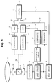
- Fig. 1 is referred to for describing a system and a method embodied in the optical disk writing system and the method for writing according to this aspect of the invention.
- Fig. 1 diagrammatically shows the optical disk writing system.
- the optical disk system shown in Fig. 1 is constituted by a laser light source 1, lenses 2 and 4, a beam splitter 3, a phase transition optical disk 5, a laser driver 6, a differentiation circuit 8, a delay circuit 9, comparators 10, 11, 15 and 16, AND circuits 17 and 18, and a pulse count circuit 21.
- the laser light source 1 constitutes a light source system which emits laser beam to produce a beam spot for writing/reading data on the phase transition optical disk 5.
- the laser light source 1 is driven by the laser driver 6.
- the lenses 2 and 4 constitute a collector which focuses the laser light emitted from the laser light source 1 as a laser beam spot on the phase transition optical disk 5.
- the beam splitter 3 constitutes a laser beam divider, which is disposed in the optical axis of the incident and divides and extracts the return light from the optical disk.
- the light emitted from the laser light source 1 is allowed to advance linearly, and the reflected light from the phase transition optical disk 5 is divided and reflected after being refracted 90°.
- the phase transition optical disk 5 is an optical disk for writing data by the irradiation of the laser light.
- the writing of data is carried out by causing the states of the writing film of the optical disk to undergo transition in response to a local temperature rise due to light absorption of the laser light.
- the laser driver 6 is a circuit portion for driving the laser light source 1 and causing the laser light to be generated.
- the differentiation circuit 8 is a circuit for extracting a 0/1 state transition point of an output signal from the laser driver 6 that drives the laser light source 1.
- the delay circuit 9 is a signal delay circuit portion for timings between the driving signal and the reflection signal.
- the comparators 10, 11, 15 and 16 constitute a comparison device for comparing the signal to be compared and the predetermined value. In this embodiment, by using these comparators, the transition states of the driving signal and the reflection signal are represented by pulse signals.
- the AND circuits 17 and 18 constitute a logical product circuitry, which finds transition states of the driving signal of the laser driver 6, the laser light emitted from the laser light source 1, and the reflection light from the phase transition optical disk 5.
- the transition states make it possible to confirm, that is to verify, the emission of the laser light and the execution of the writing.
- the pulse count circuit 21 is a circuit portion for confirming whether the write confirmation signal and the read confirmation signal are correctly present. By this confirmation, the reliability of the verification can be enhanced.
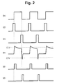
- Fig. 2 shows, in timing charts, timings of verifying operations.
- the charts show respectively timings of the signals indicated in Fig. 1.
- the output signal 57 of the AND circuit 17 is a logical product signal of the gate signal 52 with the waveform as shown in Fig. 2 and the comparator signal 55 with the waveform as shown in Fig. 2, and is represented by a symbol VL in the explanation given below.
- the output signal 58 of the AND circuit 18 is a logical product signal of the gate signal 53 with the waveform as shown in Fig. 2 and the comparator signal 56 with the waveform as shown in Fig. 2, and is represented by a symbol VT in the explanation given below.
- the delayed writing signal 61 is made a gate signal, and the number of the pulses of the output signals 57 of the AND circuit 17 and the output signals 58 of the AND circuit 18, which are generated in the gate, are counted. In this counting, when both the two pulses, namely, one pulse of the signal VL and one pulse of the signal VT, are counted, it confirms that the writing has been correctly been made.
- the writing signal is delayed because the time for the laser light rising and the time necessary for the writing film to melt are taken into account.
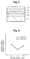
- the phase transition optical disk 5 of this example is structured as shown in Fig. 3.
- the structure was obtained by depositing ZnS-SiO 2 102 to 150 nm, Ge 2 Sb 2 Te 5 103 to 20 nm, ZnS-SiO 2 104 to 20 nm, and Al 105 to 60 nm in this sequence by sputtering on a polycarbonate substrate 101.
- (2-7)-modulated random data was written by rotating this phase transition optical disk 5 at a linear speed of 7.5 m/s and setting the writing pulse width to 50 ns.
- the writing power Pw was set to 14 to 16 mW
- the erasing power Pe was set to 7 mW
- the reading power Pr was set to 1 mW.
- the reflectivities of the writing film were 25% when the film was in the crystal state, and 8% when in the amorphous state.
- the return light dose Ic from the phase transition optical disk 5 in a crystal state of the writing film during the reading was 1.5 V
- the return light dose IA from the phase transition optical disk 5 in an amorphous state was 0.48 V.
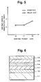
- the writing error signal generating times during the writing when CLV was set to (0.9 ⁇ Ic ⁇ Pw)/Pr while CTV was set to 0.5 ⁇ (IC+IA) ⁇ (PE)/Pr are shown in Fig. 4. Shown in Fig. 4 are results of the checking of writing errors by reading the written area after the writing as in the prior art. As is noted from Fig. 4, the detected number of writing error generation times in this example is in accord with that in the prior art example.
- the verifying was carried out by varying the reference voltage CLV and the reference voltage CTV, and the checking was made as to the optimum values of the reference voltages CLV and CTV.
- the writing error generating times detected were in accord with those in the prior art example when the condition (0.7 ⁇ Ic ⁇ Pw)/Pr ⁇ CLV(Ic ⁇ Pw)/Pr was satisfied.
- the writing error generating times detected were in accord with those in the prior art example when the condition (IA ⁇ PE)/Pr ⁇ CTV ⁇ (Ic ⁇ PE)/Pr was satisfied.
- the phase transition optical disk 5 of this example employs a structure which is obtained by depositing ZnS-SiO 2 102 to 100 nm, Ge 1 Sb 2 Te 4 103 to 25 nm, ZnS-SiO 2 104 to 20 nm, and Al 105 to 60 nm in this sequence by sputtering on a polycarbonate substrate 101.
- (2-7)-modulated random data was written by rotating the disk at a linear speed of 7.5 m/s and setting the writing pulse width of 50 ns.
- the writing power Pw was set to 16 to 18 mW
- the erasing power Pe was set to 8 mW
- the reading power Pr was set to 1 mW.
- the reflectivities of the writing film were 20% when the film was in the crystal state, and 6% when in the amorphous state.
- the return light dose Ic from the phase transition optical disk 5 in a crystal state of the writing film during the reading was 1.2 V
- the return light dose IA from the phase transition optical disk 5 in an amorphous state was 0.36 V.
- the writing error signal generating times with respect to the writing power during the writing when the reference voltage CLV was set to (0.8 ⁇ Ic ⁇ Pw)/Pr while the reference voltage CTV was set to 0.4 ⁇ (Ic+IA) ⁇ (Pe)/Pr are shown in Fig. 5. Shown in Fig. 5 are results of the checking of writing errors by reading the written area after the writing as in the prior art. As is noted from Fig. 5, the detected number of writing error generation times in this example is in accord with that in the prior art example.
- the verifying was carried out by varying the reference voltage CLV and the reference voltage CTV, and the checking was made as to the optimum values of the reference voltages CLV and CTV.
- the writing error generating times detected were in accord with those in the prior art example when the condition (0.7 ⁇ Ic ⁇ Pw)/Pr ⁇ CLV ⁇ (Ic ⁇ Pw)/Pr was satisfied.
- the writing error generating times detected were in accord with those in the prior art example when the condition (IA ⁇ PE)/Pr ⁇ CTV ⁇ (Ic ⁇ PE)/Pr was satisfied.
- the phase transition optical disk 5 of this example is structured as shown in Fig. 6.
- the structure was obtained by depositing Au 112 to 10 nm, ZnS-SiO 2 113 to 150 nm, Ge 2 Sb 2 Te 5 114 to 20 nm, ZnS-SiO 2 115 to 45 nm, and Al 116 to 100 nm in this sequence by sputtering on a polycarbonate substrate 111.
- (2-7)-modulated random data was written by rotating the disk at a linear speed of 7.5 m/s and setting the writing pulse width of 50 ns.
- the writing power Pw was set to 18 to 20 mW
- the erasing power Pe was set to 9 mW
- the reading power Pr was set to 1 mW.
- the reflectivity in the amorphous state is higher, and the reflectivity when the writing film was in the crystal state was 10% and that when the writing film was in the amorphous state was 30%.
- the return light dose Ic from the phase transition optical disk 5 in a crystal state of the writing film during the reading was 0.6 V, and the return light dose IA from the phase transition optical disk 5 in the amorphous state was 1.8 V.
- the verifying was carried out by varying the reference voltage CLV and the reference voltage CTV, and the checking was made as to the optimum values of the reference voltages CLV and CTV.
- the writing error generating times detected were in accord with those in the prior art example when the condition (0.7 ⁇ Ic ⁇ Pw)/Pr ⁇ CLV ⁇ (Ic ⁇ Pw)/Pr was satisfied.
- the writing error generating times detected were in accord with those in the prior art example when the condition (Ic ⁇ PE)/Pr ⁇ CTV ⁇ (IA ⁇ PE)/Pr was satisfied.
- the intensity monitor output IL of the return light from the optical disk at the rise of the writing signal may be checked.
- the light dose monitor output IT of the return light from the optical disk at the fall of the writing signal may be checked.
- the relation among the reflectivities to be satisfied is Rc>Rm>Ra
- the relation among the reflectivities to be satisfied is Rc ⁇ Rm ⁇ Ra
- Rc is a reflectivity of the writing film when it is in a crystal state
- Ra is a reflectivity when the same is in an amorphous state
- Rm is a reflectivity when the same is in a melted state.
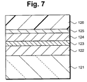
- Fig. 7 shows in a sectional view a structure of an optical data writing medium according to the invention.
- a transparent substrate 121 there are deposited a first protective film 122, a writing film 123, a second protective film 124 and a reflection film 125.
- a reflection film 125 On the reflection film 125, ultraviolet-setting resin 126 is coated for protective purpose.
- the substrate 121 employs glass or plastic in a disk shape.
- the first protective film 122 and the second protective film 124 employ such dielectric materials as SiO 2 , Si 3 N 4 , AlN, TiC 2 , ZnS, and Zns-SiO 2 .
- the writing film 123 employs GeSbTe, InSbTe, InSe, InTe, AsTeGe, TeOx-GeSn, TeSeSn, SbSeBi, BiSeGe, etc. of chalcogenide system.
- Si and Ge are used in particular.
- a metal film is used as the reflection film 125
- Al, Au or alloys of AlTi or alloys of AuPd, etc. can be used.
- the feature of this second aspect of the invention resides in that fact that, of three reflectivities of the data writing film respectively in a crystal state, in an amorphous state, and in a melted state, the reflectivity in the crystal state and the reflectivity in the melted state are different from each other, and the reflectivity in the amorphous state and the reflectivity in the melted state are different from each other.
- Figs. 8A, 8B and 8C are for use in explaining a writing/reading method, particularly a verifying operation during writing, by using an optical data writing medium according to the invention.
- the writing film 133 is heated to above the melting point.
- the numeral 131 in Fig. 8C indicates a region where the writing film has been heated to above the melting point.
- the monitored signals of the reflection light doses then obtained are divided into two kinds in their states as shown respectively in Fig. 8A and Fig. 8B. That is, the state in Fig.
- FIG. 8A is a state wherein the reflectivity of the melt region 131 of the writing film is higher than that of the region 132 that immediately precedes the melt region 131
- the state shown in Fig. 8B is a state wherein the reflectivity of the melt region 131 is lower than that of the region 132 that immediately precedes the melt region 131.
- the reasons for the monitor signals resulting in the waveforms as shown in Figs. 8A and 8B are that, with the writing power irradiation, the light reflection dose becomes higher during the time period corresponding to the writing pulse irradiation, that there is a time lag between the writing power irradiation start time and the melt start time, and that the laser light 130 has a constant beam diameter.
- Fig. 9 is a graph showing the reflectivities obtained for an amorphous state, a crystal state and a melt state with respect to one structure of the optical data writing medium according to the invention.
- the structure includes a transparent substrate 121, a first protective film 122 formed on the transparent substrate 121, a phase transition type data writing film 123 formed on the first protective film 122, a second protective film 124 formed on the writing film 123, and a reflection film 125 of a high refraction dielectric formed on the second protective film 124. It also includes a layer of ultraviolet-setting resin 126.
- As the high refraction dielectric reflection film 125 Si is used in this structure. A wavelength is 690 nm.
- the transparent substrate employs polycarbonate
- the first protective film employs ZnS-SiO 2 .
- the thickness of the phase transition type data writing film of GeSbTe is 10 nm
- that of the second protective film of ZnS-SiO 2 is 18 nm
- that of the reflective film of Si is 60 nm.
- a ZnS-SiO 2 layer of 120 nm thick as an interference layer and an ultraviolet-setting resin layer of 10 ⁇ m are formed on the resulting structure.
- the reflectivity of the crystal state and that of the melt state become essentially the same as each other so that it is difficult to distinguish one from the other.
- the reflectivities respectively of the three states namely, the crystal, amorphous and melt states, are distinctly different from one another, thereby making it possible to distinguish the melt state from the other states.
- Fig. 10 is a graph showing the reflectivities obtained for an amorphous state, a crystal state and a melt state with respect to another structure of the optical data writing medium according to the invention.
- the structure includes a transparent substrate 121, a first protective film 122 formed on the transparent substrate 121, a phase transition type data writing film 123 formed on the first protective film 122, a second protective film 124 formed on the writing film, and a reflection film 125 of a metal formed on the second protective film 124. It also includes a layer of ultraviolet-setting resin 126.
- Al is used in this structure.
- a wavelength is 690 nm.
- the transparent substrate employs polycarbonate
- the first protective film employs ZnS-SiO 2 .
- the thickness of the phase transition type data writing film of GeSbTe is 12 nm
- that of the second protective film of ZnS-SiO 2 is 20 nm
- that of the reflective film of Al is 60 nm.
- an ultraviolet-setting resin layer of 10 ⁇ m is formed on the resulting structure.
- the reflectivities in the three states that is, crystal, amorphous and melt states, are distinctly different one another in the neighborhood of 130 nm, of 210 nm and of 300 nm of the thicknesses of the first protective film, and this enables the confirmation of the melt state.
- Fig. 11 is a graph showing the reflectivities obtained for an amorphous state, a crystal state and a melt state with respect to still another structure of the optical data writing medium according to the invention.
- the structure includes a transparent substrate 121, a first protective film 122 formed on the transparent substrate 121, a phase transition type data writing film 123 formed on the first protective film 122, a second protective film 124 formed on the writing film 123, and a reflection film 125 of a metal formed on the second protective film 124. It also includes a layer of ultraviolet-setting resin 126.
- As the metal reflection film 125 a thin film of Au is used in this structure. A wavelength is 690 nm.
- the transparent substrate employs polycarbonate
- the first protective film employs ZnS-SiO 2 .
- the thickness of the phase transition type data writing film of GeSbTe is 40 nm
- that of the second protective film of ZnS-SiO 2 is 140 nm
- that of the reflective film of Au is 10 nm.
- an ultraviolet-setting resin layer of 10 ⁇ m is formed on the resulting structure.
- the reflectivities in the amorphous and melt states are approximately the same and not distinguishable in the neighborhood of 100 nm and 260 nm of the thicknesses of the first protective film, but the reflectivities in the three states are significantly different from one another where the first protective film has thicknesses other than above thicknesses, thus enabling the confirmation of the melt state.
- the optical data writing medium for this test is prepared as follows:
- the transparent substrate employs a polycarbonate substrate having preformed grooves and having a diameter of 130 mm and a thickness of 1.2 mm.
- a ZnS-SiO 2 film of 150 nm thick as a first protective film By sputtering, there are formed a ZnS-SiO 2 film of 150 nm thick as a first protective film, a Ge 2 Sb 2 Te 5 film of 10 nm thick as a writing film, a ZnS-SiO 2 film of 18 nm thick as a second protective film, and an Si reflection film of 60 nm thick as a reflection film. Also, a ZnS-SiO 2 film of 120 nm thick is formed as an interference layer. Further, by spin coating, an ultraviolet-setting resin film of 10 ⁇ m thick is deposited.
- the overwrite is carried out and the reproduced waveforms during the writing are monitored.
- the reproduced waveforms during the writing have shown changes in the reflectivity in the melt portion, thus enabling the confirmation of the writing state as being in order.
- the optical data writing medium for this comparison test is prepared as follows:
- the transparent substrate employs a polycarbonate substrate having preformed-grooves and having a diameter of 130 mm and a thickness of 1.2 mm.
- a ZnS-SiO 2 film of 100 nm thick as a first protective film By sputtering, there are formed a ZnS-SiO 2 film of 100 nm thick as a first protective film, a Ge 2 Sb 2 Te 5 film of 10 nm thick as a writing film, a ZnS-SiO 2 film of 18 nm thick as a second protective film, and an Si film of 60 nm thick as a reflection film. Also, a ZnS-SiO 2 film of 120 nm thick is formed as an interference layer. Further, by spin coating, an ultraviolet-setting resin film of 10 ⁇ m thick is deposited.
- the overwrite is carried out and the reproduced waveforms during the writing are monitored. From these reproduced waveforms, it has not been possible to observe a distinction between the melt portion and the crystal portion, that is, it has not been possible to confirm the propriety of the writing state.
- the optical data writing medium for this test is prepared as follows:
- the transparent substrate employs a polycarbonate substrate having preformed-grooves and having a diameter of 130 mm and a thickness of 1.2 mm.
- a ZnS-SiO 2 film of 130 nm thick as a first protective film By sputtering, there are formed a ZnS-SiO 2 film of 130 nm thick as a first protective film, a Ge 2 Sb 2 Te 5 film of 12 nm thick as a writing film, a ZnS-SiO 2 film of 20 nm thick as a second protective film, and an Al film of 60 nm thick as a reflection film.
- an ultraviolet-setting resin film of 10 ⁇ m thick is deposited.
- the overwrite is carried out and the reproduced waveforms during the writing are monitored.
- the reproduced waveforms during the writing have shown an increase in the reflectivity in the melt portion as compared with that in the crystal portion, thus enabling the confirmation of the writing state as being in order.
- the optical data writing medium for this comparison test is prepared as follows:
- the transparent substrate employs a polycarbonate substrate having preformed-grooves and having a diameter of 130 mm and a thickness of 1.2 mm.
- a ZnS-SiO 2 film of 180 nm thick as a first protective film By sputtering, there are formed a ZnS-SiO 2 film of 180 nm thick as a first protective film, a Ge 2 Sb 2 Te 5 film of 12 run thick as a writing film, a ZnS-SiO 2 film of 20 nm thick as a second protective film, and an Al film of 60 nm thick as a reflection film. Further, by spin coating, an ultraviolet-setting resin film of 10 ⁇ m thick is deposited.
- the overwrite is carried out and the reproduced waveforms during the writing are monitored. From these reproduced waveforms, it has not been possible to observe a distinction between the melt portion and the crystal portion, that is, it has not been possible to confirm the propriety of the writing state.
- the optical data writing medium for this test is prepared as follows:
- the transparent substrate employs a polycarbonate substrate having preformed-grooves and having a diameter of 130 mm and a thickness of 1.2 mm.
- a ZnS-SiO 2 film of 180 nm thick as a first protective film By sputtering, there are formed a ZnS-SiO 2 film of 180 nm thick as a first protective film, a Ge 2 Sb 2 Te 5 film of 40 nm thick as a writing film, a ZnS-SiO 2 film of 140 nm thick as a second protective film, and an Au film of 10 nm thick as a reflection film. Further, by spin coating, an ultraviolet-setting resin film of 10 ⁇ m thick is deposited.
- the overwrite is carried out and the reproduced waveforms during the writing are monitored.
- the reproduced waveforms during the writing have shown a decrease in the reflectivity in the melt portion as compared with that in the amorphous portion, thus enabling the confirmation of the writing state as being in order.
- the optical data writing medium for this comparison test is prepared as follows:
- the transparent substrate employs a polycarbonate substrate having preformed-grooves and having a diameter of 130 mm and a thickness of 1.2 mm.
- a ZnS-SiO 2 film of 110 nm thick as a first protective film By sputtering, there are formed a ZnS-SiO 2 film of 110 nm thick as a first protective film, a Ge 2 Sb 2 Te 5 film of 40 nm thick as a writing film, a ZnS-SiO 2 film of 140 nm thick as a second protective film, and an Au film of 10 nm thick as a reflection film. Further, by spin coating, an ultraviolet-setting resin film of 10 ⁇ m thick is deposited.
- the overwrite is carried out and the reproduced waveforms during the writing are monitored. From these reproduced waveforms, it has not been possible to observe a distinction between the melt portion and the amorphous portion, that is, it has not been possible to confirm the propriety of the writing state.
- the optical data writing medium for this test is prepared by using Ge for the reflection film instead of Si used in Example 4 with the remaining being the same as in Example 4.
- the overwrite is carried out and the reproduced waveforms during the writing are monitored.
- the reproduced waveforms during the writing have shown changes in the reflectivity in the melt portion, thus enabling the confirmation of the writing state as being in order.
- the optical data writing medium for this test is prepared by using Al-Ti for the reflection film instead of Al used in Example 5 with the remaining being the same as in Example 5.
- the overwrite is carried out and the reproduced waveforms during the writing are monitored.
- the reproduced waveforms during the writing have shown an increase in the reflectivity in the melt portion as compared with that in the crystal portion, thus enabling the confirmation of the writing state as being in order.
- a judgment circuit illustrated in Fig. 12 has been used.
- a comparator 144 receives a reading signal 141 during the writing and a comparator level 142, and it outputs a comparator output signal 143.
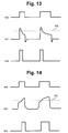
- the comparator input level with respect to the reading signal during the writing has been set as shown by 142 in Fig. 13.
- Fig. 13 shows the waveforms obtained when the writing is made under the crystal state, the waveform 140 showing the writing signal, the waveform 141 showing the reading signal during the writing, and the waveform 142 showing the verifying comparator level.
- the comparator output pulses are as shown by the waveform 143.
- the crystal state and the melt state can be distinguished from each other whereby a desired verifying output can be obtained.
- Fig. 14 shows the waveforms obtained when the writing is made under the amorphous state, the waveform 140 showing the writing signal, the waveform 141 showing the reading signal during the writing, and the waveform 142 showing the verifying comparator level.
- the comparator output pulses are as shown by the waveform 143.
- the crystal state and the melt state can be distinguished from each other whereby a desired verifying output can be obtained.
- the invention provides the structure of the medium which is suited for the simultaneous writing verifying operations of the phase transition type disk, and it also provides a writing/reading method which is featured in simultaneous writing verifying operations.
- the invention since it is possible to realize the structure of the medium in which the reflectivities in the melt, crystal and amorphous states are distinctly different from one another and the simultaneous writing verifying procedures which are suited for such medium, there is a great advantage that the data rewriting operation can be effected at a high speed. The great advantage is that the overwrite operation can be completed within one disk rotation.
- the optical disk writing system disclosed is one in which a data written on an optical data writing medium is verified essentially simultaneously with the writing on the medium.
- the written data is verified by detecting a timing of the light irradiated on the medium and by measuring return light doses at a rise and a fall of the light irradiated on the medium and comparing the doses thereof with predetermined reference values.
- the medium used is one which uses a phase transition reversible between a crystal state and an amorphous state for writing/reading/erasing of data on a data writing film includes, a first protective film (122), a phase transition type data writing film (123), a second protective film (124), a reflection film (125) formed in this order on a transparent substrate (121).
- the thickness of the first protective film is set such that, of three reflectivities of the data writing film respectively in crystal, amorphous and melted states, the reflectivity in the crystal state and the reflectivity in the melted state are made different from each other, and the reflectivity in the amorphous state and the reflectivity in the melted state are made different from each other, and the reflectivity in the amorphous state and the reflectivity in the melted state are made different from each other.
- a high speed writing operation can be carried out and an overwrite operation can be completed in one time disk rotation.
Landscapes
- Chemical & Material Sciences (AREA)
- Inorganic Chemistry (AREA)
- Optical Recording Or Reproduction (AREA)
- Optical Record Carriers And Manufacture Thereof (AREA)
Applications Claiming Priority (6)
| Application Number | Priority Date | Filing Date | Title |
|---|---|---|---|
| JP7130215A JP2770780B2 (ja) | 1995-05-29 | 1995-05-29 | 光ディスクの記録装置および記録方法 |
| JP13021595 | 1995-05-29 | ||
| JP130215/95 | 1995-05-29 | ||
| JP22932195 | 1995-09-06 | ||
| JP7229321A JPH0973660A (ja) | 1995-09-06 | 1995-09-06 | 光学的情報記録媒体ならびに記録中ベリファイ方法 |
| JP229321/95 | 1995-09-06 |
Publications (3)
| Publication Number | Publication Date |
|---|---|
| EP0745975A2 true EP0745975A2 (de) | 1996-12-04 |
| EP0745975A3 EP0745975A3 (de) | 1998-02-04 |
| EP0745975B1 EP0745975B1 (de) | 2003-09-24 |
Family
ID=26465413
Family Applications (1)
| Application Number | Title | Priority Date | Filing Date |
|---|---|---|---|
| EP96303859A Expired - Lifetime EP0745975B1 (de) | 1995-05-29 | 1996-05-29 | System und Verfahren zur gleichzeitigen Nachprüfung von optischen Aufzeichnungen von Daten |
Country Status (3)
| Country | Link |
|---|---|
| US (2) | US5798993A (de) |
| EP (1) | EP0745975B1 (de) |
| KR (1) | KR960042568A (de) |
Cited By (4)
| Publication number | Priority date | Publication date | Assignee | Title |
|---|---|---|---|---|
| EP0793223A1 (de) * | 1996-02-27 | 1997-09-03 | Ricoh Company, Ltd | Optisches Aufzeichnungsmedium |
| EP0829867A3 (de) * | 1996-09-13 | 1998-11-04 | Nec Corporation | Optisches Aufzeichnungsmedium vom Phasenwechsel-Typ und Verfahren zur Aufzeichnung mit diesem Medium |
| EP1207525A3 (de) * | 2000-11-15 | 2005-03-09 | Ricoh Company, Ltd. | Optisches Informationsaufzeichnungsverfahren mit einem verbesserten Schema zur Aufzeichnungsleistungssteuerung |
| EP1100079A4 (de) * | 1999-04-26 | 2006-08-02 | Sony Corp | Optische platte und herstellungsverfahren |
Families Citing this family (7)
| Publication number | Priority date | Publication date | Assignee | Title |
|---|---|---|---|---|
| JPH0944904A (ja) * | 1995-07-31 | 1997-02-14 | Sony Corp | 光学ディスクとその製法 |
| US6768707B1 (en) * | 1996-09-13 | 2004-07-27 | Nec Corporation | Phase-change type optical recording medium and method of optically recording with the same |
| KR100509752B1 (ko) * | 1997-08-30 | 2005-10-28 | 엘지전자 주식회사 | 기록과검증을동시에수행하는광기록/재생방법및장치 |
| JP3734621B2 (ja) * | 1998-07-03 | 2006-01-11 | 株式会社リコー | 光情報記録方法及びその装置 |
| US6537721B2 (en) * | 1999-02-15 | 2003-03-25 | Tdk Corporation | Optical recording medium and method for its initialization |
| US20070231427A1 (en) * | 2006-03-29 | 2007-10-04 | Wm Wrigley Jr. Company | Spray-formed confectionery product, apparatus and method |
| US7752585B2 (en) * | 2007-10-15 | 2010-07-06 | International Business Machines Corporation | Method, apparatus, and computer program product for stale NDR detection |
Family Cites Families (13)
| Publication number | Priority date | Publication date | Assignee | Title |
|---|---|---|---|---|
| JPS5935090B2 (ja) * | 1978-12-27 | 1984-08-27 | 株式会社日立製作所 | 情報記録装置 |
| JPS5792438A (en) * | 1980-11-28 | 1982-06-09 | Ricoh Co Ltd | Recording method by laser beam |
| JPS60145537A (ja) * | 1984-01-10 | 1985-08-01 | Nec Corp | 光学式情報記録方式及びその装置 |
| US4680594A (en) * | 1986-04-02 | 1987-07-14 | Optotech, Inc. | Single beam direct read during write and write protect system for use in an optical data storage system |
| JPH029024A (ja) * | 1988-06-28 | 1990-01-12 | Mitsubishi Electric Corp | 光学式情報記録再生装置 |
| JPH0341632A (ja) * | 1989-07-07 | 1991-02-22 | Matsushita Electric Ind Co Ltd | 光ディスク装置 |
| JP2574911B2 (ja) * | 1990-01-10 | 1997-01-22 | シャープ株式会社 | 光磁気記録方法 |
| US5242784A (en) * | 1990-07-13 | 1993-09-07 | International Business Machines Corporation | System and method for optical phase change recording |
| JPH05144112A (ja) * | 1991-11-15 | 1993-06-11 | Canon Inc | 情報記録再生装置 |
| US5517471A (en) * | 1992-01-06 | 1996-05-14 | Canon Kabushiki Kaisha | Method and apparatus for verifying recording data and for determining recording error using a detected light amount |
| JP3287648B2 (ja) * | 1993-06-07 | 2002-06-04 | 株式会社リコー | 相変化型情報記録媒体の記録同時ベリファイ方法及び相変化型情報記録ドライブ装置 |
| JPH08147744A (ja) * | 1994-11-16 | 1996-06-07 | Canon Inc | 光記録装置 |
| JP2783179B2 (ja) * | 1995-02-27 | 1998-08-06 | 日本電気株式会社 | 光学情報の記録・再生方法及び記録・再生装置 |
-
1996
- 1996-05-22 US US08/651,301 patent/US5798993A/en not_active Expired - Lifetime
- 1996-05-28 KR KR1019960018304A patent/KR960042568A/ko not_active Ceased
- 1996-05-29 EP EP96303859A patent/EP0745975B1/de not_active Expired - Lifetime
-
1998
- 1998-07-01 US US09/108,914 patent/US5906908A/en not_active Expired - Fee Related
Cited By (6)
| Publication number | Priority date | Publication date | Assignee | Title |
|---|---|---|---|---|
| EP0793223A1 (de) * | 1996-02-27 | 1997-09-03 | Ricoh Company, Ltd | Optisches Aufzeichnungsmedium |
| US6221557B1 (en) | 1996-02-27 | 2001-04-24 | Ricoh Company, Ltd. | Optical information recording medium |
| EP0829867A3 (de) * | 1996-09-13 | 1998-11-04 | Nec Corporation | Optisches Aufzeichnungsmedium vom Phasenwechsel-Typ und Verfahren zur Aufzeichnung mit diesem Medium |
| EP1100079A4 (de) * | 1999-04-26 | 2006-08-02 | Sony Corp | Optische platte und herstellungsverfahren |
| EP1207525A3 (de) * | 2000-11-15 | 2005-03-09 | Ricoh Company, Ltd. | Optisches Informationsaufzeichnungsverfahren mit einem verbesserten Schema zur Aufzeichnungsleistungssteuerung |
| US7019273B2 (en) | 2000-11-15 | 2006-03-28 | Ricoh Company, Ltd. | Optical information recording employing improved recording power control scheme |
Also Published As
| Publication number | Publication date |
|---|---|
| EP0745975B1 (de) | 2003-09-24 |
| EP0745975A3 (de) | 1998-02-04 |
| US5798993A (en) | 1998-08-25 |
| KR960042568A (ko) | 1996-12-21 |
| US5906908A (en) | 1999-05-25 |
Similar Documents
| Publication | Publication Date | Title |
|---|---|---|
| US6987720B2 (en) | Information recording and/or reproducing apparatus, information recording and/or reproducing method, and phase-change recording medium for use in the apparatus and the methods | |
| US5646924A (en) | Recording and simultaneous verifying method of phase-changing type of information recording medium | |
| US6222814B1 (en) | Recording/reproducing apparatus and method for phase-change optical disc | |
| EP0446892B1 (de) | Verfahren zur optischen Aufzeichnung von Daten auf einem Medium | |
| EP0729136B1 (de) | Verfahren und Vorrichtung zur Aufzeichnung und Wiedergabe von optischen Informationen unter Verwendung eines optischen Phasenwechselmediums | |
| EP0745975B1 (de) | System und Verfahren zur gleichzeitigen Nachprüfung von optischen Aufzeichnungen von Daten | |
| US6333913B1 (en) | Optical recording medium and optical recording method | |
| EP0683485A1 (de) | Optische Platte vom Phasenwechseltyp | |
| US5459711A (en) | Optical recording element and driving system | |
| EP0630007A1 (de) | Optisches Informationsaufzeichnungsmedium | |
| EP0335486A2 (de) | Optische Informationsaufzeichnungsmethode | |
| US5504732A (en) | Null inflection detection and pulse expand latch in an optical recording system | |
| US6456576B1 (en) | Optical recording method | |
| US6165579A (en) | Optical information recording medium and recording/reproduction method | |
| KR100298972B1 (ko) | 상변화형광기록매체및광기록매체에광학적으로기록하는방법 | |
| US5862122A (en) | Phase change optical disk and a method for recording and playbacking optical information on or from an optical disk | |
| JPH11144336A (ja) | 記録媒体の初期化方法 | |
| JP2000076653A (ja) | 情報記録装置 | |
| JP2770780B2 (ja) | 光ディスクの記録装置および記録方法 | |
| JP3220020B2 (ja) | 相変化型光ディスク媒体と情報の記録・再生方法 | |
| JPH0973660A (ja) | 光学的情報記録媒体ならびに記録中ベリファイ方法 | |
| JP2803245B2 (ja) | 情報記録再生方法 | |
| JPS63183624A (ja) | 情報の記録および消去方法 | |
| JPH06195713A (ja) | 光記録の記録方法 | |
| JP2602245B2 (ja) | 情報の記録・再生方法 |
Legal Events
| Date | Code | Title | Description |
|---|---|---|---|
| PUAI | Public reference made under article 153(3) epc to a published international application that has entered the european phase |
Free format text: ORIGINAL CODE: 0009012 |
|
| AK | Designated contracting states |
Kind code of ref document: A2 Designated state(s): GB NL |
|
| PUAL | Search report despatched |
Free format text: ORIGINAL CODE: 0009013 |
|
| 17P | Request for examination filed |
Effective date: 19971110 |
|
| AK | Designated contracting states |
Kind code of ref document: A3 Designated state(s): GB NL |
|
| 17Q | First examination report despatched |
Effective date: 20020308 |
|
| RTI1 | Title (correction) |
Free format text: SYSTEM AND METHOD FOR SIMULTANEOUSLY VERIFYING OPTICAL DATA WRITING |
|
| GRAH | Despatch of communication of intention to grant a patent |
Free format text: ORIGINAL CODE: EPIDOS IGRA |
|
| GRAS | Grant fee paid |
Free format text: ORIGINAL CODE: EPIDOSNIGR3 |
|
| GRAA | (expected) grant |
Free format text: ORIGINAL CODE: 0009210 |
|
| AK | Designated contracting states |
Kind code of ref document: B1 Designated state(s): GB NL |
|
| REG | Reference to a national code |
Ref country code: GB Ref legal event code: FG4D |
|
| PLBE | No opposition filed within time limit |
Free format text: ORIGINAL CODE: 0009261 |
|
| STAA | Information on the status of an ep patent application or granted ep patent |
Free format text: STATUS: NO OPPOSITION FILED WITHIN TIME LIMIT |
|
| 26N | No opposition filed |
Effective date: 20040625 |
|
| PGFP | Annual fee paid to national office [announced via postgrant information from national office to epo] |
Ref country code: GB Payment date: 20100329 Year of fee payment: 15 |
|
| PGFP | Annual fee paid to national office [announced via postgrant information from national office to epo] |
Ref country code: NL Payment date: 20100518 Year of fee payment: 15 |
|
| REG | Reference to a national code |
Ref country code: NL Ref legal event code: V1 Effective date: 20111201 |
|
| GBPC | Gb: european patent ceased through non-payment of renewal fee |
Effective date: 20110529 |
|
| PG25 | Lapsed in a contracting state [announced via postgrant information from national office to epo] |
Ref country code: NL Free format text: LAPSE BECAUSE OF NON-PAYMENT OF DUE FEES Effective date: 20111201 |
|
| PG25 | Lapsed in a contracting state [announced via postgrant information from national office to epo] |
Ref country code: GB Free format text: LAPSE BECAUSE OF NON-PAYMENT OF DUE FEES Effective date: 20110529 |