EP0630007A1 - Optisches Informationsaufzeichnungsmedium - Google Patents
Optisches Informationsaufzeichnungsmedium Download PDFInfo
- Publication number
- EP0630007A1 EP0630007A1 EP19940109224 EP94109224A EP0630007A1 EP 0630007 A1 EP0630007 A1 EP 0630007A1 EP 19940109224 EP19940109224 EP 19940109224 EP 94109224 A EP94109224 A EP 94109224A EP 0630007 A1 EP0630007 A1 EP 0630007A1
- Authority
- EP
- European Patent Office
- Prior art keywords
- layer
- recording
- reflectivity
- thickness
- crystalline state
- Prior art date
- Legal status (The legal status is an assumption and is not a legal conclusion. Google has not performed a legal analysis and makes no representation as to the accuracy of the status listed.)
- Granted
Links
- 230000003287 optical effect Effects 0.000 title claims abstract description 104
- 239000010410 layer Substances 0.000 claims abstract description 153
- 238000002310 reflectometry Methods 0.000 claims abstract description 76
- 239000011241 protective layer Substances 0.000 claims abstract description 54
- 239000000758 substrate Substances 0.000 claims abstract description 29
- 239000000126 substance Substances 0.000 claims abstract description 15
- 230000001419 dependent effect Effects 0.000 claims abstract description 3
- 239000002356 single layer Substances 0.000 claims abstract description 3
- VYPSYNLAJGMNEJ-UHFFFAOYSA-N Silicium dioxide Chemical compound O=[Si]=O VYPSYNLAJGMNEJ-UHFFFAOYSA-N 0.000 claims description 35
- 229910052681 coesite Inorganic materials 0.000 claims description 19
- 229910052906 cristobalite Inorganic materials 0.000 claims description 19
- 229910052682 stishovite Inorganic materials 0.000 claims description 19
- 229910052905 tridymite Inorganic materials 0.000 claims description 19
- 239000000377 silicon dioxide Substances 0.000 claims description 16
- 235000012239 silicon dioxide Nutrition 0.000 claims description 16
- PBCFLUZVCVVTBY-UHFFFAOYSA-N tantalum pentoxide Inorganic materials O=[Ta](=O)O[Ta](=O)=O PBCFLUZVCVVTBY-UHFFFAOYSA-N 0.000 claims description 7
- 229920005989 resin Polymers 0.000 claims description 6
- 239000011347 resin Substances 0.000 claims description 6
- 229910052751 metal Inorganic materials 0.000 claims description 5
- 239000002184 metal Substances 0.000 claims description 5
- 239000000203 mixture Substances 0.000 claims description 4
- 229910052782 aluminium Inorganic materials 0.000 claims description 3
- 229910052737 gold Inorganic materials 0.000 claims description 3
- 229910052581 Si3N4 Inorganic materials 0.000 claims description 2
- 239000000654 additive Substances 0.000 claims description 2
- 230000000996 additive effect Effects 0.000 claims description 2
- 239000000956 alloy Substances 0.000 claims description 2
- 229910045601 alloy Inorganic materials 0.000 claims description 2
- 150000004770 chalcogenides Chemical class 0.000 claims description 2
- 229910052804 chromium Inorganic materials 0.000 claims description 2
- 150000001875 compounds Chemical class 0.000 claims description 2
- 230000001747 exhibiting effect Effects 0.000 claims description 2
- -1 for example Inorganic materials 0.000 claims description 2
- 150000002739 metals Chemical class 0.000 claims description 2
- 229910052750 molybdenum Inorganic materials 0.000 claims description 2
- 150000004767 nitrides Chemical class 0.000 claims description 2
- SBIBMFFZSBJNJF-UHFFFAOYSA-N selenium;zinc Chemical compound [Se]=[Zn] SBIBMFFZSBJNJF-UHFFFAOYSA-N 0.000 claims description 2
- 239000004065 semiconductor Substances 0.000 claims description 2
- LIVNPJMFVYWSIS-UHFFFAOYSA-N silicon monoxide Inorganic materials [Si-]#[O+] LIVNPJMFVYWSIS-UHFFFAOYSA-N 0.000 claims description 2
- 229910052715 tantalum Inorganic materials 0.000 claims description 2
- 229910052719 titanium Inorganic materials 0.000 claims description 2
- 229910052721 tungsten Inorganic materials 0.000 claims description 2
- 229920005668 polycarbonate resin Polymers 0.000 claims 2
- 239000004431 polycarbonate resin Substances 0.000 claims 2
- 230000000052 comparative effect Effects 0.000 description 20
- 238000000034 method Methods 0.000 description 15
- 238000010586 diagram Methods 0.000 description 12
- 239000011159 matrix material Substances 0.000 description 9
- 230000001965 increasing effect Effects 0.000 description 8
- 238000004519 manufacturing process Methods 0.000 description 7
- 239000004417 polycarbonate Substances 0.000 description 7
- 229920000515 polycarbonate Polymers 0.000 description 7
- 238000004544 sputter deposition Methods 0.000 description 5
- 238000005259 measurement Methods 0.000 description 4
- 238000001816 cooling Methods 0.000 description 2
- 230000002708 enhancing effect Effects 0.000 description 2
- 230000006978 adaptation Effects 0.000 description 1
- 230000015556 catabolic process Effects 0.000 description 1
- 238000006731 degradation reaction Methods 0.000 description 1
- 230000000694 effects Effects 0.000 description 1
- 230000004927 fusion Effects 0.000 description 1
- 239000011521 glass Substances 0.000 description 1
- 238000002360 preparation method Methods 0.000 description 1
- 238000003860 storage Methods 0.000 description 1
- 238000002834 transmittance Methods 0.000 description 1
Images




Classifications
-
- G—PHYSICS
- G11—INFORMATION STORAGE
- G11B—INFORMATION STORAGE BASED ON RELATIVE MOVEMENT BETWEEN RECORD CARRIER AND TRANSDUCER
- G11B7/00—Recording or reproducing by optical means, e.g. recording using a thermal beam of optical radiation by modifying optical properties or the physical structure, reproducing using an optical beam at lower power by sensing optical properties; Record carriers therefor
- G11B7/24—Record carriers characterised by shape, structure or physical properties, or by the selection of the material
- G11B7/241—Record carriers characterised by shape, structure or physical properties, or by the selection of the material characterised by the selection of the material
- G11B7/252—Record carriers characterised by shape, structure or physical properties, or by the selection of the material characterised by the selection of the material of layers other than recording layers
- G11B7/253—Record carriers characterised by shape, structure or physical properties, or by the selection of the material characterised by the selection of the material of layers other than recording layers of substrates
- G11B7/2533—Record carriers characterised by shape, structure or physical properties, or by the selection of the material characterised by the selection of the material of layers other than recording layers of substrates comprising resins
- G11B7/2534—Record carriers characterised by shape, structure or physical properties, or by the selection of the material characterised by the selection of the material of layers other than recording layers of substrates comprising resins polycarbonates [PC]
-
- G—PHYSICS
- G11—INFORMATION STORAGE
- G11B—INFORMATION STORAGE BASED ON RELATIVE MOVEMENT BETWEEN RECORD CARRIER AND TRANSDUCER
- G11B7/00—Recording or reproducing by optical means, e.g. recording using a thermal beam of optical radiation by modifying optical properties or the physical structure, reproducing using an optical beam at lower power by sensing optical properties; Record carriers therefor
- G11B7/004—Recording, reproducing or erasing methods; Read, write or erase circuits therefor
- G11B7/0055—Erasing
- G11B7/00557—Erasing involving phase-change media
-
- G—PHYSICS
- G11—INFORMATION STORAGE
- G11B—INFORMATION STORAGE BASED ON RELATIVE MOVEMENT BETWEEN RECORD CARRIER AND TRANSDUCER
- G11B7/00—Recording or reproducing by optical means, e.g. recording using a thermal beam of optical radiation by modifying optical properties or the physical structure, reproducing using an optical beam at lower power by sensing optical properties; Record carriers therefor
- G11B7/24—Record carriers characterised by shape, structure or physical properties, or by the selection of the material
-
- G—PHYSICS
- G11—INFORMATION STORAGE
- G11B—INFORMATION STORAGE BASED ON RELATIVE MOVEMENT BETWEEN RECORD CARRIER AND TRANSDUCER
- G11B7/00—Recording or reproducing by optical means, e.g. recording using a thermal beam of optical radiation by modifying optical properties or the physical structure, reproducing using an optical beam at lower power by sensing optical properties; Record carriers therefor
- G11B7/24—Record carriers characterised by shape, structure or physical properties, or by the selection of the material
- G11B7/241—Record carriers characterised by shape, structure or physical properties, or by the selection of the material characterised by the selection of the material
- G11B7/242—Record carriers characterised by shape, structure or physical properties, or by the selection of the material characterised by the selection of the material of recording layers
- G11B7/243—Record carriers characterised by shape, structure or physical properties, or by the selection of the material characterised by the selection of the material of recording layers comprising inorganic materials only, e.g. ablative layers
-
- G—PHYSICS
- G11—INFORMATION STORAGE
- G11B—INFORMATION STORAGE BASED ON RELATIVE MOVEMENT BETWEEN RECORD CARRIER AND TRANSDUCER
- G11B7/00—Recording or reproducing by optical means, e.g. recording using a thermal beam of optical radiation by modifying optical properties or the physical structure, reproducing using an optical beam at lower power by sensing optical properties; Record carriers therefor
- G11B7/24—Record carriers characterised by shape, structure or physical properties, or by the selection of the material
- G11B7/241—Record carriers characterised by shape, structure or physical properties, or by the selection of the material characterised by the selection of the material
- G11B7/252—Record carriers characterised by shape, structure or physical properties, or by the selection of the material characterised by the selection of the material of layers other than recording layers
- G11B7/258—Record carriers characterised by shape, structure or physical properties, or by the selection of the material characterised by the selection of the material of layers other than recording layers of reflective layers
-
- G—PHYSICS
- G11—INFORMATION STORAGE
- G11B—INFORMATION STORAGE BASED ON RELATIVE MOVEMENT BETWEEN RECORD CARRIER AND TRANSDUCER
- G11B7/00—Recording or reproducing by optical means, e.g. recording using a thermal beam of optical radiation by modifying optical properties or the physical structure, reproducing using an optical beam at lower power by sensing optical properties; Record carriers therefor
- G11B7/24—Record carriers characterised by shape, structure or physical properties, or by the selection of the material
- G11B7/241—Record carriers characterised by shape, structure or physical properties, or by the selection of the material characterised by the selection of the material
- G11B7/242—Record carriers characterised by shape, structure or physical properties, or by the selection of the material characterised by the selection of the material of recording layers
- G11B7/243—Record carriers characterised by shape, structure or physical properties, or by the selection of the material characterised by the selection of the material of recording layers comprising inorganic materials only, e.g. ablative layers
- G11B2007/24302—Metals or metalloids
- G11B2007/24316—Metals or metalloids group 16 elements (i.e. chalcogenides, Se, Te)
-
- G—PHYSICS
- G11—INFORMATION STORAGE
- G11B—INFORMATION STORAGE BASED ON RELATIVE MOVEMENT BETWEEN RECORD CARRIER AND TRANSDUCER
- G11B7/00—Recording or reproducing by optical means, e.g. recording using a thermal beam of optical radiation by modifying optical properties or the physical structure, reproducing using an optical beam at lower power by sensing optical properties; Record carriers therefor
- G11B7/24—Record carriers characterised by shape, structure or physical properties, or by the selection of the material
- G11B7/241—Record carriers characterised by shape, structure or physical properties, or by the selection of the material characterised by the selection of the material
- G11B7/252—Record carriers characterised by shape, structure or physical properties, or by the selection of the material characterised by the selection of the material of layers other than recording layers
- G11B7/254—Record carriers characterised by shape, structure or physical properties, or by the selection of the material characterised by the selection of the material of layers other than recording layers of protective topcoat layers
- G11B7/2542—Record carriers characterised by shape, structure or physical properties, or by the selection of the material characterised by the selection of the material of layers other than recording layers of protective topcoat layers consisting essentially of organic resins
-
- G—PHYSICS
- G11—INFORMATION STORAGE
- G11B—INFORMATION STORAGE BASED ON RELATIVE MOVEMENT BETWEEN RECORD CARRIER AND TRANSDUCER
- G11B7/00—Recording or reproducing by optical means, e.g. recording using a thermal beam of optical radiation by modifying optical properties or the physical structure, reproducing using an optical beam at lower power by sensing optical properties; Record carriers therefor
- G11B7/24—Record carriers characterised by shape, structure or physical properties, or by the selection of the material
- G11B7/241—Record carriers characterised by shape, structure or physical properties, or by the selection of the material characterised by the selection of the material
- G11B7/252—Record carriers characterised by shape, structure or physical properties, or by the selection of the material characterised by the selection of the material of layers other than recording layers
- G11B7/258—Record carriers characterised by shape, structure or physical properties, or by the selection of the material characterised by the selection of the material of layers other than recording layers of reflective layers
- G11B7/2585—Record carriers characterised by shape, structure or physical properties, or by the selection of the material characterised by the selection of the material of layers other than recording layers of reflective layers based on aluminium
-
- G—PHYSICS
- G11—INFORMATION STORAGE
- G11B—INFORMATION STORAGE BASED ON RELATIVE MOVEMENT BETWEEN RECORD CARRIER AND TRANSDUCER
- G11B7/00—Recording or reproducing by optical means, e.g. recording using a thermal beam of optical radiation by modifying optical properties or the physical structure, reproducing using an optical beam at lower power by sensing optical properties; Record carriers therefor
- G11B7/24—Record carriers characterised by shape, structure or physical properties, or by the selection of the material
- G11B7/241—Record carriers characterised by shape, structure or physical properties, or by the selection of the material characterised by the selection of the material
- G11B7/252—Record carriers characterised by shape, structure or physical properties, or by the selection of the material characterised by the selection of the material of layers other than recording layers
- G11B7/258—Record carriers characterised by shape, structure or physical properties, or by the selection of the material characterised by the selection of the material of layers other than recording layers of reflective layers
- G11B7/2595—Record carriers characterised by shape, structure or physical properties, or by the selection of the material characterised by the selection of the material of layers other than recording layers of reflective layers based on gold
-
- Y—GENERAL TAGGING OF NEW TECHNOLOGICAL DEVELOPMENTS; GENERAL TAGGING OF CROSS-SECTIONAL TECHNOLOGIES SPANNING OVER SEVERAL SECTIONS OF THE IPC; TECHNICAL SUBJECTS COVERED BY FORMER USPC CROSS-REFERENCE ART COLLECTIONS [XRACs] AND DIGESTS
- Y10—TECHNICAL SUBJECTS COVERED BY FORMER USPC
- Y10S—TECHNICAL SUBJECTS COVERED BY FORMER USPC CROSS-REFERENCE ART COLLECTIONS [XRACs] AND DIGESTS
- Y10S428/00—Stock material or miscellaneous articles
- Y10S428/913—Material designed to be responsive to temperature, light, moisture
-
- Y—GENERAL TAGGING OF NEW TECHNOLOGICAL DEVELOPMENTS; GENERAL TAGGING OF CROSS-SECTIONAL TECHNOLOGIES SPANNING OVER SEVERAL SECTIONS OF THE IPC; TECHNICAL SUBJECTS COVERED BY FORMER USPC CROSS-REFERENCE ART COLLECTIONS [XRACs] AND DIGESTS
- Y10—TECHNICAL SUBJECTS COVERED BY FORMER USPC
- Y10S—TECHNICAL SUBJECTS COVERED BY FORMER USPC CROSS-REFERENCE ART COLLECTIONS [XRACs] AND DIGESTS
- Y10S430/00—Radiation imagery chemistry: process, composition, or product thereof
- Y10S430/146—Laser beam
-
- Y—GENERAL TAGGING OF NEW TECHNOLOGICAL DEVELOPMENTS; GENERAL TAGGING OF CROSS-SECTIONAL TECHNOLOGIES SPANNING OVER SEVERAL SECTIONS OF THE IPC; TECHNICAL SUBJECTS COVERED BY FORMER USPC CROSS-REFERENCE ART COLLECTIONS [XRACs] AND DIGESTS
- Y10—TECHNICAL SUBJECTS COVERED BY FORMER USPC
- Y10T—TECHNICAL SUBJECTS COVERED BY FORMER US CLASSIFICATION
- Y10T428/00—Stock material or miscellaneous articles
- Y10T428/21—Circular sheet or circular blank
-
- Y—GENERAL TAGGING OF NEW TECHNOLOGICAL DEVELOPMENTS; GENERAL TAGGING OF CROSS-SECTIONAL TECHNOLOGIES SPANNING OVER SEVERAL SECTIONS OF THE IPC; TECHNICAL SUBJECTS COVERED BY FORMER USPC CROSS-REFERENCE ART COLLECTIONS [XRACs] AND DIGESTS
- Y10—TECHNICAL SUBJECTS COVERED BY FORMER USPC
- Y10T—TECHNICAL SUBJECTS COVERED BY FORMER US CLASSIFICATION
- Y10T428/00—Stock material or miscellaneous articles
- Y10T428/31504—Composite [nonstructural laminate]
- Y10T428/31678—Of metal
Definitions
- This invention relates to an optical information-recording medium for recording information by utilizing changes in optical properties thereof induced by different thermal histories of a rise and a fall of temperature caused by irradiation of a laser beam thereon, i.e. a phase change optical disk.
- phase change optical disk is adapted to perform recording and erasing by a change in the optical properties thereof induced by a thermal history of a rise and a fall of temperature caused by irradiation of a laser beam thereon.
- this type of optical disk is adapted to record information or overwrite new information on old one, by modulating optical energy irradiated thereon between two intensity levels correspondent to two states thereof which can be optically discriminated from each other.
- the higher level will be referred to as a recording power level, while the lower level as an erasing power level.
- Reproduction of information is performed normally by detecting changes in reflectivity or transmittance between the two states.
- a recording medium used in the phase change optical disk is generally higher in absorptivity when it is in the amorphous state than when it is in the crystalline state, and therefore, in performing overwriting by the mark edge recording method, the length or position of each recording mark recorded varies depending on whether the recording mark is recorded on the amorphous state or on the crystalline state, and this results in degraded overwriting characteristics, such as increased recording jitter, and a lower erasability resulting from modulation of an overwriting signal, which occurs in dependence on the existing or recorded information.
- the layer structure of a phase change optical disk should be designed such that absorptivity in the crystalline state becomes higher than one in the amorphous state.
- Fig. 1 shows the relationship between the thickness of a single Au layer formed on a glass substrate and reflectivity of the layer exhibited in reflecting light irradiated on the substrate.
- the invention disclosed in Japanese Unexamined Patent Publication (Kokai) No. 1-149238 obtains desired effects by reducing the thickness of the Au layer as the reflective layer to 20 nm, thereby lowering the reflectivity of the reflective layer.
- the resulting reflectivity largely depends on the layer thickness, when the layer thickness is so small as 20 nm or has a value close thereto. Therefore, if the layer thickness is largely deviated from a specified value, this causes a large undesirable change in the reflectivity of the reflective layer, resulting in a large amount of deviation from the desired optical properties of the recording medium.
- the manufacturing tolerance of the thickness of the reflective layer is so strict or close. Further, when the thickness of the reflective layer is small, the cooling rate of the medium becomes low, and hence thermal load thereon becomes large, which can cause a problem of degraded characteristics occurring with repetition of recording and erasing.
- the difference in reflectivity between the amorphous state and the crystalline state is detected for reproduction of information, and to increase the signal strength, it is required to increase the difference in reflectivity between the amorphous state and the crystalline state.
- the recording medium is more often used after being crystallized. Therefore, the reflectivity in the crystalline state is set to a higher value, and the absorptivity of the crystalline state is set to a lower value when the disk is arranged to include a reflective layer.
- the present invention provides an optical information-recording medium including a substrate, and a lower protective layer, a recording layer, an upper protective layer and a reflective layer, formed on the substrate, the recording layer exhibiting different optical properties dependent on different thermal histories of a rise and a fall in temperature caused by irradiation of a laser beam on the substrate, wherein the optical information-recording medium has a layer structure constructed such that reflectivity of the optical information-recording medium and a phase of light reflected therefrom vary with the change in the optical properties of the recording layer, with absorptivity of light of the recording layer being larger when the recording layer is in a crystalline state than when the recording layer is in an amorphous state, and at the same time, reflectivity exhibited when the recording layer is in the crystalline state being 10 % or higher; and wherein the reflective layer has a thickness set such that a value of reflectivity of the reflective layer exhibited in the form of a single layer is 90% or more of a value of reflectivity of a
- the optical information-recording medium of the present invention is constructed such that the reflectivity of the medium and the phase of reflected light change with a change in the optical properties of the recording layer, and therefore, it is possible to obtain a high-quality signal without increasing the difference in reflectivity between the crystalline state and the amorphous state. Therefore, the absorptivity of the recording layer exhibited when the recording layer is in the crystalline state can be enhanced more easily, which provides excellent overwriting characteristics in mark edge recording. Further, the reflectivity exhibited in the crystalline state of the recording layer is high, and hence the servo-mechanism is stabilized.
- the thickness of the reflective layer is set to such a range as indicated by the arrows in Fig. 1, in which the reflectivity of the reflective layer exhibits a value of 90% or higher of the reflectivity of a bulk form of the substance used for the reflective layer. Therefore, the reflectivity of the reflective layer is not easily changed, while permitting a large manufacturing tolerance of the reflective layer.
- a transparent substrate 1 On a transparent substrate 1, there are formed a lower protective layer 2, a recording layer 3, an upper protective layer 4 and a reflective layer 5.
- the recording layer 3 is formed of a substance which has its optical properties changed depending on different thermal histories of a rise and a fall of temperature caused by irradiation of a laser beam thereto at different energy levels, e.g. a compound containing a chalcogen-series atom, for example, Se and Te.
- the lower protective layer 2 and the upper protective layer 4 are layers for protecting the recording layer from heat, and at the same time used for optical interference.
- the lower protective layer 2 and the upper protective layer 4 are formed of a single substance selected from nitrides, for example, Si3N4 and AlN, which are transparent, oxides, for example, SiO, SiO2 and Ta2O5, and chalcogenides, for example, ZnS, ZnSe, and MnS, or a mixture thereof.
- the reflective layer 5 may be formed of a single substance selected from metals, for example, Al, Au, Ti, Cr, Mo, W and Ta.
- a mixture of such a substance and an additive, or an alloy of such a substance may be used for control of the reflectivity and thermal diffusivity of the reflective layer 5, and for enhancing adherence of the same to adjacent layers.
- semiconductors for example, Si and Ge, which are high in refractive index, can be used as well.
- Reflectivity and the optical phase difference between the reflected lights can be determined from optical constants of the recording layer, the protective layers, and the reflective layer, and thicknesses of the layers, by a matrix method (refer, for example, to Masao Tsuruta, "Applied Optics II", Applied Physics Engineering Selections Vol. 2, Baifu-kan, 1990, Chapter 4).
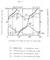
- the optical constants of the lower protective layer and the upper protective layer were 2.2-i0.0, and the optical constant of the recording layer was 5.89-i3.47 in the crystalline state, and 4.60-i1.06 in the amorphous state, and that of the reflective layer was 2.83-i7.75.
- the thickness of the lower protective layer was within a range of 43 nm to 137 nm, and a range of 232 nm to 300 nm, absorptivity was higher in the crystalline state than in the amorphous state, with reflectivity in the crystalline state being 10% or higher. Further, in this range, the optical phase difference between reflected light from the crystalline state and reflected light from the amorphous state was large, with the absolute value thereof being equal to 90° or larger.
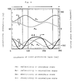
- Specimens of the recording medium were prepared in the same manner as in Example 1 with the exception that the thickness of the recording layer was set to 15 nm. Results of calculations are shown in Fig. 4. As indicated by arrows in Fig. 4, when the thickness of the lower protective layer was within a range of 5 nm to 67 nm, a range of 102 nm to 256 nm, and a range of 291 nm to 300 nm, the absorptivity was higher in the crystalline state than in the amorphous state, with reflectivity in the crystalline state being 10 % or higher.
- Specimens of the recording medium were prepared in the same manner as in Example 1 with the exception that the thickness of the recording layer was set to 25 nm. Results of calculations are shown in Fig. 5. As indicated by arrows in Fig. 5, when the thickness of the lower protective layer was within a range of 56 nm to 107 nm and a range of 244 nm to 296 nm, absorptivity was higher in the crystalline state than in the amorphous state, with reflectivity in the crystalline state being 10 % or higher.
- Specimens of the recording medium were prepared in the same manner as in Example 1 with the exception that the thickness of the recording layer was set to 30 nm. Results of calculations are shown in Fig. 6. As indicated by arrows in Fig. 6, when the thickness of the lower protective layer was within a range of 42 nm to 122 nm and a range of 230 nm to 300 nm, absorptivity was higher in the crystalline state than in the amorphous state, with reflectivity in the crystalline state being 10 % or higher.
- Specimens of the recording medium were prepared in the same manner as in Example 1 with the exception that the thickness of the recording layer was set to 40 nm. Results of calculations are shown in Fig. 7. As indicated by arrows in Fig. 7, when the thickness of the lower protective layer was within a range of 35 nm to 118 nm and a range of 222 nm to 300 nm, absorptivity was higher in the crystalline state than in the amorphous state, with reflectivity in the crystalline state being 10 % or higher.
- Reflectivity of light irradiated on the substrate was 11.6% in the amorphous state, and 13.5% in the crystalline state.
- Optical calculations by the matrix method show that absorptivity was 67.7% in the amorphous state, and 80.5% in the crystalline state, and the optical phase difference between reflected light from the crystalline and reflected light from the amorphous state was -151.8°.
- a specimen of the recording medium was prepared in the same manner as in Example 6 with the exception that the thickness of the lower protective layer of ZnS-20at%SiO2 was set to 130 nm. Reflectivity of light irradiated on the substrate was 9.2% in the amorphous state, and 22.6% in the crystalline state. Optical calculations by the matrix method show that absorptivity was 69.5% in the amorphous state, and 72.1% in the crystalline state, and the optical phase difference between reflected light from the crystalline and reflected light from the amorphous state was -107.6°.
- a specimen of a recording medium as Comparative Example 1 was prepared, which had a large difference in reflectivity between the crystalline state and the amorphous state, and a small optical phase difference between reflected light from the crystalline state and reflected light from the amorphous state, and exhibited a higher absorptivity in the amorphous state than in the crystalline state, in the same manner as in Example 6 with the exception that the thickness of a lower protective layer of ZnS-20at%Si02 was set to 180 nm. Reflectivity of light irradiated on the substrate was 4.2% in the amorphous state, and 33.9% in the crystalline state.
- Example 6 in which reflectivity in the crystalline state was the smallest, reflectivity was equal to 13.5%, i.e. a value higher than 10%, so that there did not arise a problem of unstable servo-mechanism.
- Fig. 8 shows results of measurement of jitter in cases where after a signal of 3.7 MHz was once recorded, and then a signal of 2.12 MHz was overwritten thereon. It is recognized that compared with Comparative Example 1, the jitter became smaller in the order of Example 7, and Example 6.
- Example 6 and Example 7 however, the rate of temperature rise in the crystalline sate and that of temperature rise in the amorphous state were made equal to each other to thereby reduce variation in the recording conditions, which contributed to reduction of the difference between the leading edge jitter and the trailing edge jitter.
- Example 6 and Comparative Example 2 The overwriting characteristics were measured under the following conditions: a linear velocity of 11.3 m/s; a recording frequency of 3.7 MHz; duty for writing pulse of 45%; and recording power of 12 mW and erasing power of 6.5 mW for Example 6, and recording power of 11 mW and erasing power of 6 mW for Comparative Example 2. Results of measurement are shown in Fig. 9. In the case of Example 6, even after overwriting performed 106 times, jitter was not increased, whereas in the case of Comparative Example 2, jitter started to increase from a time point at which overwriting was performed approximately 104 times.
- the thickness of the reflective layer was as thin as 20 nm, and hence the cooling rate was low, resulting in an increased thermal load on the medium, which more readily caused degradation of the characteristics of the recording medium when recording and erasing were repeatedly carried out.
- Comparative Example 2 there were prepared specimens of a disk, with exception that the thickness of a reflective layer is varied, and then reliability in repetition of overwriting was measured.
- the relationship between the thickness of the reflective layer and the amount of increase in jitter detected after overwriting was repeatedly performed 106 times is shown in Fig. 10. It is understood that if the reflective layer had a thickness of 40 nm or larger, jitter did not increase even after overwriting was performed 106 times.
- a specimen of a disk was prepared as Comparative Example 3, which had such a layer arrangement as exhibits very little difference in reflectivity and a large optical phase difference between reflected light from the crystalline state and reflected light from the amorphous state, as disclosed in Japanese Unexamined Patent Publication (Kokai) No. 2-73537, Japanese Unexamined Patent Publication (Kokai) No. 2-113451, and Japanese Unexamined Patent Publication (Kokai) No. 3-41638.
- Reflectivity of light irradiated on the substrate was 5.8% in the amorphous state, and 13.6% in the crystalline state.
- Optical calculations by the matrix method show that absorptivity was 79.8% in the amorphous state, and 78.9% in the crystalline state, and the optical phase difference between reflected light from the crystalline state and reflected light from the amorphous state was -85.5°.
- Optical constants used in the optical calculations were 1.96-i0.0 for Ta2O5 of the lower protective layer and the upper protective layer, 4.60-i1.60 for Ge1Sb4Te7 of the recording layer in the amorphous state, and 5.70-i3.52 for the same in the crystalline state.
- Example 9 As to the specimen of Example 9, a signal of 3.7 MHz was recorded, and then a signal of 2.12 MHz was overwritten thereon. Measurement of jitter was performed, obtaining more excellent results than those obtained with Comparative Example 1, similarly to Example 3. Jitter did not increase even after overwriting was performed 106 times.
- the present invention is very effective in reducing overwriting jitter occurring with a phase change optical disk.
- the adaptation of a light source such that it emits a laser beam having a reduced wavelength is effective, since it permits reduction of the diameter of the laser beam.
- specimens of Example 10 were prepared by forming, on a substrate of polycarbonate, one upon another in the order mentioned hereafter, a lower protective layer of ZnS-20at%Si02 with a thickness in a range of 100 nm to 300 nm, a recording layer of Ge2Sb2Te5 with a thickness of 15 nm, an upper protective layer of ZnS-20at%SiO2 with a thickness of 20 nm, and a reflective layer of Al with a thickness of 60 nm.
- Optical constants of the lower protective layer and the upper protective layer were 2.1-i0.0 for the wavelength of 690 nm, and an optical constant of the recording layer 4.03-i3.87 in the crystalline state, and 3.79-i1.36 in the amorphous state, and an optical constant of the reflective layer 1.73-i7.96.
- the thickness of the lower protective layer was within a range of 210 nm to 277 nm, absorptivity was higher in the crystalline state than in the amorphous state, with reflectivity in the crystalline state being 10% or higher.
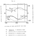
- Specimens of the recording medium were prepared in the same manner as in Example 10 with the exception that the thickness of the upper protective layer was set to 30 nm. Results of calculations are shown in Fig. 12. As indicated by arrows in Fig. 12, when the thickness of the lower protective layer was within a range of 210 nm to 265 nm, absorptivity was higher in the crystalline state than in the amorphous state, with reflectivity in the crystalline state being 10 % or higher. Further, in this range, the optical phase difference between reflected light from the crystalline state and reflected light from the amorphous state is large, assuming a value of 90°.
- Reflectivity of light irradiated on the substrate was 13.6% in the amorphous state, and 14.9% in the crystalline state.
- Optical calculations by the matrix method show that absorptivity was 74.2% in the amorphous state, and 81.0% in the crystalline state, and the optical phase difference between reflected light from the crystalline state and reflected light from the amorphous state was -105.2°.
- a specimen of a recording medium as Comparative Example 4 was prepared, which had a large difference in reflectivity, and a small optical phase difference between reflected light from the crystalline state and reflected light from the amorphous state, and exhibited a higher absorptivity in the amorphous state than in the crystalline state, in the same manner as in Example 12 with the exception that the thickness of the lower protective layer of ZnS-20at%Si02 was set to 160 nm. Reflectivity of light irradiated on the substrate was 11.9% in the amorphous state, and 32.5% in the crystalline state.
- Example 12 and Comparative Example 4 Overwriting characteristics of Example 12 and Comparative Example 4 were evaluated. Each of specimens in the form of a disk was rotated at a speed of 9.42 m/s. An optical head used in recording and erasing had an numerical aperture (NA) for the objective lens of 0.55, through which a laser beam having a wavelength of 690 nm was emitted. The reproducing power was set to 1.0 mW. The specimens were exposed to the laser beam in advance before recording to thereby change the recording layer from the amorphous state, in which it had been immediately after preparation of the laminate of layers, to the crystalline state.
- NA numerical aperture
- Example 12 Even in Example 12, in which reflectivity in the crystalline state was relatively small, the reflectivity was equal to 14.9%, which is a value higher than 10%, so that there did not arise a problem of unstable servo-mechanism. Jitter was measured, after a signal of 2.90 MHz was once recorded and then a signal of 1.81 MHz was overwritten thereon.
- leading edge jitter detected for first recording was 1.3 ns
- trailing edge jitter detected for the same was 1.2 ns
- leading edge jitter detected for overwriting was 2.0 ns
- trailing edge jitter for the same was 1.90 ns, showing that amounts of increase in jitter caused by overwriting were small.
- the optical information-recording medium of the present invention is constructed such that reflectivity and phase of reflected light change with a change in the optical properties of a recording layer, which enables a highquality signal to be obtained without increasing the difference in reflectivity between the crystalline state and the amorphous state. Therefore, the absorptivity of the recording layer exhibited when the recording layer is in the crystalline state can be enhanced more easily, which provides excellent overwriting characteristics in mark edge recording. Further, since reflectivity exhibited in the crystalline state of the recording layer is high, the servo-mechanism can be stabilized.
- the thickness of the reflective layer is set to such a range as indicated by the arrows in Fig. 1, in which the reflectivity of the reflective layer is 90% or higher of the reflectivity of a bulk form of the substance used for the reflective layer. Therefore, the reflectivity of the reflective layer is not readily varied, permitting a large manufacturing tolerance of the reflective layer.
- the manufacturing tolerance of layers in respect of thickness thereof becomes large, and at the same time excellent overwriting characteristics in mark edge recording can be obtained, with a high reliability in repetition of recording and erasing.
Landscapes
- Chemical & Material Sciences (AREA)
- Inorganic Chemistry (AREA)
- Optical Record Carriers And Manufacture Thereof (AREA)
- Thermal Transfer Or Thermal Recording In General (AREA)
Applications Claiming Priority (6)
| Application Number | Priority Date | Filing Date | Title |
|---|---|---|---|
| JP145299/93 | 1993-06-17 | ||
| JP14529993 | 1993-06-17 | ||
| JP14529993 | 1993-06-17 | ||
| JP1187294A JP2812181B2 (ja) | 1993-06-17 | 1994-02-03 | 光学的情報記録媒体 |
| JP1187294 | 1994-02-03 | ||
| JP11872/94 | 1994-02-03 |
Publications (2)
| Publication Number | Publication Date |
|---|---|
| EP0630007A1 true EP0630007A1 (de) | 1994-12-21 |
| EP0630007B1 EP0630007B1 (de) | 2000-10-25 |
Family
ID=26347392
Family Applications (1)
| Application Number | Title | Priority Date | Filing Date |
|---|---|---|---|
| EP19940109224 Expired - Lifetime EP0630007B1 (de) | 1993-06-17 | 1994-06-15 | Optisches Informationsaufzeichnungsmedium |
Country Status (4)
| Country | Link |
|---|---|
| US (1) | US5506022A (de) |
| EP (1) | EP0630007B1 (de) |
| JP (1) | JP2812181B2 (de) |
| DE (1) | DE69426171T2 (de) |
Cited By (13)
| Publication number | Priority date | Publication date | Assignee | Title |
|---|---|---|---|---|
| EP0706176A4 (de) * | 1994-03-25 | 1996-09-25 | Toray Industries | Optisches aufzeichnungsmedium und verfahren zu dessen herstellung |
| EP0779614A1 (de) * | 1995-12-11 | 1997-06-18 | Teijin Limited | Optisches Aufzeichnungsmedium mit Phasenänderung |
| EP0793223A1 (de) * | 1996-02-27 | 1997-09-03 | Ricoh Company, Ltd | Optisches Aufzeichnungsmedium |
| EP0737967A3 (de) * | 1995-03-28 | 1997-09-24 | Toray Industries | Optische Aufzeichnungsmedien und Verfahren zur Aufzeichnung darauf |
| US5719006A (en) * | 1994-10-19 | 1998-02-17 | Nec Corporation | Optical information recording medium |
| EP0847049A2 (de) * | 1996-12-05 | 1998-06-10 | Mitsubishi Chemical Corporation | Optisches Informationsaufzeichnungsmedium |
| EP0706177A4 (de) * | 1994-03-25 | 1998-09-02 | Toray Industries | Optisches aufzeichnungsmedium |
| EP0883116A3 (de) * | 1997-06-03 | 1999-02-10 | Nec Corporation | Optische Aufzeichnungsmedien |
| EP0919996A2 (de) * | 1997-11-25 | 1999-06-02 | Samsung Electronics Co., Ltd. | Optische Phasenwechselplatte mit einer reflektierenden Schicht aus Edelmetal sowie optisches Aufzeichnungssystem |
| EP0867868A3 (de) * | 1997-03-27 | 1999-10-06 | Mitsubishi Chemical Corporation | Optisches Informationsaufzeichnugsmedium |
| EP0887791A4 (de) * | 1996-02-28 | 1999-10-06 | Asahi Chemical Ind | Verfahren zum entwurf eines optischen aufzeichnungsmediums vom phasenwechseltyp sowie optisches aufzeichnungsmedium vom phasenwechseltyp |
| US6300039B1 (en) | 1994-03-25 | 2001-10-09 | Toray Industries, Inc. | Optical recording medium |
| RU2174715C1 (ru) * | 2000-11-01 | 2001-10-10 | Лапин Юрий Константинович | Носитель информации оптического запоминающего устройства и способ записи оптической информации на него |
Families Citing this family (5)
| Publication number | Priority date | Publication date | Assignee | Title |
|---|---|---|---|---|
| JP3138661B2 (ja) * | 1996-10-24 | 2001-02-26 | 日本電気株式会社 | 相変化型光ディスク |
| US5972459A (en) * | 1997-04-25 | 1999-10-26 | Sony Corporation | Optical recording medium and optical disk apparatus |
| JPH11203725A (ja) * | 1998-01-16 | 1999-07-30 | Nec Corp | 相変化光ディスク |
| US6426936B1 (en) | 1998-01-27 | 2002-07-30 | Ricoh Company, Ltd. | Phase-change medium usable in phase-difference tracking |
| US6191384B1 (en) | 1998-05-05 | 2001-02-20 | Tapematic S.P.A. | Apparatus for trimming dye coated on a recordable disc substrate and related method |
Citations (4)
| Publication number | Priority date | Publication date | Assignee | Title |
|---|---|---|---|---|
| EP0319037A2 (de) * | 1987-12-04 | 1989-06-07 | Matsushita Electric Industrial Co., Ltd. | Optisches Informationsaufzeichnungsmedium |
| JPH0273537A (ja) * | 1988-09-09 | 1990-03-13 | Matsushita Electric Ind Co Ltd | 光学的情報記録媒体 |
| EP0360466A1 (de) * | 1988-09-09 | 1990-03-28 | Matsushita Electric Industrial Co., Ltd. | Optischer Datenaufzeichnungsträger sowie zugehöriges Aufzeichnungs- und Wiedergabeverfahren |
| JPH02113451A (ja) * | 1988-10-21 | 1990-04-25 | Matsushita Electric Ind Co Ltd | 光学的情報記録媒体 |
Family Cites Families (5)
| Publication number | Priority date | Publication date | Assignee | Title |
|---|---|---|---|---|
| JPH0746442B2 (ja) * | 1986-06-30 | 1995-05-17 | 松下電器産業株式会社 | 光学情報記録媒体 |
| JPH01113451A (ja) * | 1987-10-27 | 1989-05-02 | Dainippon Toryo Co Ltd | 塗料用樹脂組成物 |
| DE68921325T2 (de) * | 1988-12-28 | 1995-09-21 | Matsushita Electric Ind Co Ltd | Medium für Datenspeicherung. |
| JPH07109654B2 (ja) * | 1989-07-07 | 1995-11-22 | 松下電器産業株式会社 | 光学的情報記録媒体およびその情報記録再生方法 |
| JPH03224790A (ja) * | 1990-01-31 | 1991-10-03 | Toshiba Corp | 情報記録媒体 |
-
1994
- 1994-02-03 JP JP1187294A patent/JP2812181B2/ja not_active Expired - Fee Related
- 1994-06-15 DE DE69426171T patent/DE69426171T2/de not_active Expired - Fee Related
- 1994-06-15 EP EP19940109224 patent/EP0630007B1/de not_active Expired - Lifetime
- 1994-06-16 US US08/260,827 patent/US5506022A/en not_active Expired - Lifetime
Patent Citations (5)
| Publication number | Priority date | Publication date | Assignee | Title |
|---|---|---|---|---|
| EP0319037A2 (de) * | 1987-12-04 | 1989-06-07 | Matsushita Electric Industrial Co., Ltd. | Optisches Informationsaufzeichnungsmedium |
| JPH01149238A (ja) * | 1987-12-04 | 1989-06-12 | Matsushita Electric Ind Co Ltd | 光学的情報記録媒体 |
| JPH0273537A (ja) * | 1988-09-09 | 1990-03-13 | Matsushita Electric Ind Co Ltd | 光学的情報記録媒体 |
| EP0360466A1 (de) * | 1988-09-09 | 1990-03-28 | Matsushita Electric Industrial Co., Ltd. | Optischer Datenaufzeichnungsträger sowie zugehöriges Aufzeichnungs- und Wiedergabeverfahren |
| JPH02113451A (ja) * | 1988-10-21 | 1990-04-25 | Matsushita Electric Ind Co Ltd | 光学的情報記録媒体 |
Cited By (21)
| Publication number | Priority date | Publication date | Assignee | Title |
|---|---|---|---|---|
| EP0706176A4 (de) * | 1994-03-25 | 1996-09-25 | Toray Industries | Optisches aufzeichnungsmedium und verfahren zu dessen herstellung |
| US6300039B1 (en) | 1994-03-25 | 2001-10-09 | Toray Industries, Inc. | Optical recording medium |
| US5840466A (en) * | 1994-03-25 | 1998-11-24 | Toray Industries, Inc. | Optical recording media and their production methods |
| EP0706177A4 (de) * | 1994-03-25 | 1998-09-02 | Toray Industries | Optisches aufzeichnungsmedium |
| US5900347A (en) * | 1994-10-19 | 1999-05-04 | Nec Corporation | Optical information recording medium |
| US5719006A (en) * | 1994-10-19 | 1998-02-17 | Nec Corporation | Optical information recording medium |
| US6140011A (en) * | 1994-10-19 | 2000-10-31 | Nec Corporation | Optical information recording medium |
| EP0737967A3 (de) * | 1995-03-28 | 1997-09-24 | Toray Industries | Optische Aufzeichnungsmedien und Verfahren zur Aufzeichnung darauf |
| EP0779614A1 (de) * | 1995-12-11 | 1997-06-18 | Teijin Limited | Optisches Aufzeichnungsmedium mit Phasenänderung |
| US5912103A (en) * | 1995-12-11 | 1999-06-15 | Teijin Limited | Phase change optical recording medium |
| EP0793223A1 (de) * | 1996-02-27 | 1997-09-03 | Ricoh Company, Ltd | Optisches Aufzeichnungsmedium |
| US6221557B1 (en) | 1996-02-27 | 2001-04-24 | Ricoh Company, Ltd. | Optical information recording medium |
| US6149999A (en) * | 1996-02-28 | 2000-11-21 | Asahi Kasei Kogyo Kabushiki Kaisha | Method of designing a phase-change optical recording medium, and a phase-change optical recording medium |
| EP0887791A4 (de) * | 1996-02-28 | 1999-10-06 | Asahi Chemical Ind | Verfahren zum entwurf eines optischen aufzeichnungsmediums vom phasenwechseltyp sowie optisches aufzeichnungsmedium vom phasenwechseltyp |
| EP0847049A2 (de) * | 1996-12-05 | 1998-06-10 | Mitsubishi Chemical Corporation | Optisches Informationsaufzeichnungsmedium |
| EP0867868A3 (de) * | 1997-03-27 | 1999-10-06 | Mitsubishi Chemical Corporation | Optisches Informationsaufzeichnugsmedium |
| EP1396851A3 (de) * | 1997-03-27 | 2004-03-17 | Mitsubishi Chemical Corporation | Optisches Informationsaufzeichnungsmedium |
| US6117511A (en) * | 1997-06-03 | 2000-09-12 | Nec Corporation | Optical recording media |
| EP0883116A3 (de) * | 1997-06-03 | 1999-02-10 | Nec Corporation | Optische Aufzeichnungsmedien |
| EP0919996A2 (de) * | 1997-11-25 | 1999-06-02 | Samsung Electronics Co., Ltd. | Optische Phasenwechselplatte mit einer reflektierenden Schicht aus Edelmetal sowie optisches Aufzeichnungssystem |
| RU2174715C1 (ru) * | 2000-11-01 | 2001-10-10 | Лапин Юрий Константинович | Носитель информации оптического запоминающего устройства и способ записи оптической информации на него |
Also Published As
| Publication number | Publication date |
|---|---|
| EP0630007B1 (de) | 2000-10-25 |
| DE69426171D1 (de) | 2000-11-30 |
| JPH0793804A (ja) | 1995-04-07 |
| JP2812181B2 (ja) | 1998-10-22 |
| DE69426171T2 (de) | 2001-04-05 |
| US5506022A (en) | 1996-04-09 |
Similar Documents
| Publication | Publication Date | Title |
|---|---|---|
| EP0630007B1 (de) | Optisches Informationsaufzeichnungsmedium | |
| EP0265971B1 (de) | Verfahren zur optischen Informationsaufzeichnung | |
| US5900347A (en) | Optical information recording medium | |
| EP0888616B1 (de) | Optisches aufzeichnungsmedium mit phasenwechsel-aufzeichnungsschicht | |
| US20040157158A1 (en) | Optical recording medium | |
| EP0319037B1 (de) | Optisches Informationsaufzeichnungsmedium | |
| US6333913B1 (en) | Optical recording medium and optical recording method | |
| JPH0778354A (ja) | 情報記録媒体およびそれを用いた記録方法 | |
| US5631895A (en) | Optical information recording medium | |
| JP3080739B2 (ja) | 光学的情報記録媒体および光学的情報記録消去再生方法 | |
| US5273861A (en) | Optical information recording medium, method of making an optical information recording medium and method of recording/reproducing optical information | |
| JPH07105574A (ja) | 光情報記録媒体 | |
| JP3180813B2 (ja) | 光学的情報記録媒体 | |
| EP1302934A2 (de) | Optisches Aufzeichnungsmedium, Methode zu dessen Messung und Methode zur optischen Aufzeichnung/ zum optischen Abspielen von Information | |
| US5862122A (en) | Phase change optical disk and a method for recording and playbacking optical information on or from an optical disk | |
| US6117511A (en) | Optical recording media | |
| JP2663843B2 (ja) | 光学情報記録媒体 | |
| JPH05151574A (ja) | 光学的情報記録消去方式 | |
| JP3087598B2 (ja) | 光記録媒体 | |
| JPH11144319A (ja) | 光学的情報記録媒体及び記録再生方法 | |
| JP2803245B2 (ja) | 情報記録再生方法 | |
| JP2982329B2 (ja) | 情報光記録媒体とその記録再生方法 | |
| KR20020000630A (ko) | 소거가능성이 증가되는 광 기록 매체 | |
| JPH09265658A (ja) | 光記録媒体 | |
| JPH09265657A (ja) | 光記録媒体 |
Legal Events
| Date | Code | Title | Description |
|---|---|---|---|
| PUAI | Public reference made under article 153(3) epc to a published international application that has entered the european phase |
Free format text: ORIGINAL CODE: 0009012 |
|
| 17P | Request for examination filed |
Effective date: 19941005 |
|
| AK | Designated contracting states |
Kind code of ref document: A1 Designated state(s): DE FR GB NL |
|
| 17Q | First examination report despatched |
Effective date: 19980512 |
|
| GRAG | Despatch of communication of intention to grant |
Free format text: ORIGINAL CODE: EPIDOS AGRA |
|
| GRAG | Despatch of communication of intention to grant |
Free format text: ORIGINAL CODE: EPIDOS AGRA |
|
| GRAG | Despatch of communication of intention to grant |
Free format text: ORIGINAL CODE: EPIDOS AGRA |
|
| GRAH | Despatch of communication of intention to grant a patent |
Free format text: ORIGINAL CODE: EPIDOS IGRA |
|
| GRAH | Despatch of communication of intention to grant a patent |
Free format text: ORIGINAL CODE: EPIDOS IGRA |
|
| GRAA | (expected) grant |
Free format text: ORIGINAL CODE: 0009210 |
|
| AK | Designated contracting states |
Kind code of ref document: B1 Designated state(s): DE FR GB NL |
|
| REF | Corresponds to: |
Ref document number: 69426171 Country of ref document: DE Date of ref document: 20001130 |
|
| ET | Fr: translation filed | ||
| PLBE | No opposition filed within time limit |
Free format text: ORIGINAL CODE: 0009261 |
|
| STAA | Information on the status of an ep patent application or granted ep patent |
Free format text: STATUS: NO OPPOSITION FILED WITHIN TIME LIMIT |
|
| 26N | No opposition filed | ||
| REG | Reference to a national code |
Ref country code: GB Ref legal event code: IF02 |
|
| PGFP | Annual fee paid to national office [announced via postgrant information from national office to epo] |
Ref country code: NL Payment date: 20090615 Year of fee payment: 16 |
|
| PGFP | Annual fee paid to national office [announced via postgrant information from national office to epo] |
Ref country code: GB Payment date: 20090610 Year of fee payment: 16 Ref country code: DE Payment date: 20090615 Year of fee payment: 16 |
|
| REG | Reference to a national code |
Ref country code: NL Ref legal event code: V1 Effective date: 20110101 |
|
| GBPC | Gb: european patent ceased through non-payment of renewal fee |
Effective date: 20100615 |
|
| REG | Reference to a national code |
Ref country code: FR Ref legal event code: ST Effective date: 20110228 |
|
| PG25 | Lapsed in a contracting state [announced via postgrant information from national office to epo] |
Ref country code: DE Free format text: LAPSE BECAUSE OF NON-PAYMENT OF DUE FEES Effective date: 20110101 |
|
| PG25 | Lapsed in a contracting state [announced via postgrant information from national office to epo] |
Ref country code: FR Free format text: LAPSE BECAUSE OF NON-PAYMENT OF DUE FEES Effective date: 20100630 Ref country code: NL Free format text: LAPSE BECAUSE OF NON-PAYMENT OF DUE FEES Effective date: 20110101 |
|
| PG25 | Lapsed in a contracting state [announced via postgrant information from national office to epo] |
Ref country code: GB Free format text: LAPSE BECAUSE OF NON-PAYMENT OF DUE FEES Effective date: 20100615 |
|
| PGFP | Annual fee paid to national office [announced via postgrant information from national office to epo] |
Ref country code: FR Payment date: 20090611 Year of fee payment: 16 |