EP0746144A2 - Halbleiterbildsensor des Types CCD - Google Patents
Halbleiterbildsensor des Types CCD Download PDFInfo
- Publication number
- EP0746144A2 EP0746144A2 EP96108795A EP96108795A EP0746144A2 EP 0746144 A2 EP0746144 A2 EP 0746144A2 EP 96108795 A EP96108795 A EP 96108795A EP 96108795 A EP96108795 A EP 96108795A EP 0746144 A2 EP0746144 A2 EP 0746144A2
- Authority
- EP
- European Patent Office
- Prior art keywords
- vertical shift
- output register
- photo
- horizontal output
- signal charges
- Prior art date
- Legal status (The legal status is an assumption and is not a legal conclusion. Google has not performed a legal analysis and makes no representation as to the accuracy of the status listed.)
- Withdrawn
Links
Images







Classifications
-
- H—ELECTRICITY
- H10—SEMICONDUCTOR DEVICES; ELECTRIC SOLID-STATE DEVICES NOT OTHERWISE PROVIDED FOR
- H10F—INORGANIC SEMICONDUCTOR DEVICES SENSITIVE TO INFRARED RADIATION, LIGHT, ELECTROMAGNETIC RADIATION OF SHORTER WAVELENGTH OR CORPUSCULAR RADIATION
- H10F39/00—Integrated devices, or assemblies of multiple devices, comprising at least one element covered by group H10F30/00, e.g. radiation detectors comprising photodiode arrays
- H10F39/10—Integrated devices
- H10F39/12—Image sensors
- H10F39/15—Charge-coupled device [CCD] image sensors
-
- H—ELECTRICITY
- H04—ELECTRIC COMMUNICATION TECHNIQUE
- H04N—PICTORIAL COMMUNICATION, e.g. TELEVISION
- H04N25/00—Circuitry of solid-state image sensors [SSIS]; Control thereof
- H04N25/70—SSIS architectures; Circuits associated therewith
- H04N25/71—Charge-coupled device [CCD] sensors; Charge-transfer registers specially adapted for CCD sensors
- H04N25/73—Charge-coupled device [CCD] sensors; Charge-transfer registers specially adapted for CCD sensors using interline transfer [IT]
Definitions
- the present invention relates to a charge coupled device (CCD)type solid state image pickup device.
- CCD charge coupled device
- a prior art CCD type solid state image pickup device includes two-dimensionally arranged photo/electro conversion portions, a plurality of vertical shift registers each connected to one column of the photo/electro conversion portions, and a horizontal output register connected to the vertical shift registers, signal charges of every two of each column of the photo/electro conversion portions are mixed within the vertical shift registers, to creat a mixed signal charge. Then, the mixed signal charge corresponding to two of the photo/electro conversion portions is transferred within the horizontal output register. Thus, one scanning line is formed by every two rows of the photo/electro conversion portions. This will be explained later in detail.
- a CCD type solid state image pickup device including two-dimensionally arranged photo/electro conversion portions, a plurality of vertical shift registers each connected to one column of the photo/electro conversion portions, and a horizontal output register connected to the vertical shift registers
- signal charges of every four of each column of the photo/electro conversion portions are mixed within the vertical shift registers or within the vertical shift registers and the horizontal output register, to create a mixed signal charge.
- the mixed signal charge corresponding to four of the photo/electro conversion portions is transferred within the horizontal output register.
- one scanning line is formed by every four rows of the photo/electro conversion portions. This increases the ratio of a width to a length of transfer electrodes of the vertical shift registers.
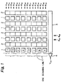
- Fig. 1 is a plan view illustrating a prior art CCD type solid state image pickup device
- light is incident to two-dimensionally arranged photo/electro conversion portions 1 formed by photo diodes, and as a result, signal charges obtained by the photo/electro conversion portions 1 are transferred to vertical shift registers 2.
- the signal charges are further transferred via a horizontal output register 3 to a signal charge output register 4 which generates an output voltage V out .
- the vertical shift registers 2 are operated by four-phase transfer pulse signals ⁇ V1 , ⁇ V2 , ⁇ V3 and ⁇ V4
- the horizontal output register 3 is operated by two-phase transfer pulse signals ⁇ H1 and ⁇ H2 .
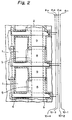
- each of the photo/electro conversion portions 1 includes a P + -type impurity diffusion region and an N-type impurity diffusion region formed on a P-type well region of a N-type semiconductor substrate.
- the vertical shift registers 2 include N-type buried channels formed on the P-type well region.
- read gate regions 5 Provided between the photo/electro conversion portions 1 and the vertical shift registers 2 are read gate regions 5. Every column of the photo/electro portions 1 and the vertical shift registers 2 are isolated from the other columns by a P + -type channel stopper region 6.
- the transfer electrodes 8 and 9 are provided for each column of the photo/electro conversion portions 1.
- the transfer electrodes 8 also serve as read gates for the read gate regions 5.
- the transfer electrodes 9 are made of a first polycrystalline silicon layer, and the transfer electrodes 8 are made of a second polycrystalline silicon layer.
- bus lines 10-1, 10-2, 10-3 and 10-4 made of aluminum are provided and connected to the transfer electrodes 8 and 9.
- the transfer pulse signals ⁇ V1 , ⁇ V2 , ⁇ V3 and ⁇ V4 are supplied to the bus lines 10-1, 10-2, 10-3 and 10-4, respectively.
- the operation of the device of Fig. 1 is interlaced scanning.
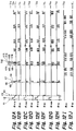
- the transfer pulse signals ⁇ V1 , ⁇ V2 , ⁇ V3 and ⁇ V4 are V L , V M , V H and V L , respectively, as shown in Figs. 3A, 3B, 3C and 3D.
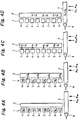
- the signal charges Q A , Q C , Q E and Q G are read out to the vertical shift register 2 as shown in Fig. 4B.
- the transfer pulse signals ⁇ V1 , ⁇ V2 , ⁇ V3 and ⁇ V4 are V H , V L , V L and V M , respectively, as shown in Figs. 3A, 3B, 3C and 3D.
- the signal charges Q E , Q D , Q F and Q H are read out to the vertical shift register 2 as shown in Fig. 4C.
- the charges Q B , Q D , Q F and Q H are added to the charges Q A , Q C , Q E and Q G , respectively, to form signal charges Q A + Q B , Q C + Q D , Q E + Q F and Q G + Q H .
- the transfer pulse signals ⁇ V1 , ⁇ V2 , ⁇ V3 and ⁇ V4 are V M , V M , V M and V L , respectively, as shown in Figs. 3A, 3B, 3C and 3D, and as a result, the potential wells are deep as shaded at time t1 in Fig. 5.
- the transfer pulse signals ⁇ V1 , ⁇ V2 , ⁇ V3 and ⁇ V4 are V L , V M , V M and V L , respectively, as shown in Figs. 3A, 3B, 3C and 3D, and as a result, the potential wells are deep as shaded at time t2 in Fig. 5.
- the transfer pulse signals ⁇ V1 , ⁇ V2 , ⁇ V3 and ⁇ V4 are V L , V L , V M and V M , respectively, as shown in Figs. 3A, 3B, 3C and 3D, and as a result, the potential wells are deep as shaded at time t3 in Fig. 5.
- the transfer pulse signals ⁇ V1 , ⁇ V2 , ⁇ V3 and ⁇ V4 are V M , V L , V L and V M , respectively, as shown in Figs.
- the transfer pulse signals ⁇ V1 , ⁇ V2 , ⁇ V3 and ⁇ V4 are V M , V M , V L and V L , respectively, as shown in Figs. 3A, 3B, 3C and 3D, and as a result, the potential wells are deep as shaded at time t5 in Fig. 5.
- the transfer pulse signals ⁇ V1 , ⁇ V2 , ⁇ V3 and ⁇ V4 are V L , V M , V M and V L , respectively, as shown in Figs. 3A, 3B, 3C and 3D, and as a result, the potential wells are deep as shaded at time t6 in Fig. 5.
- the vertical shift register 2 carries out a one-pixel vertical shift operation, so that the signal charge Q A + Q B is transferred to the horizontal output register 3 as shown in Fig. 4D.
- the transfer pulse signals ⁇ V1 , ⁇ V2 , ⁇ V3 and ⁇ V4 are changed at times t7, t8, t9 and t10 in the same way as at times t3, t4, t5 and t6 as shown in Figs. 3A, 3B, 3C and 3D.
- the vertical shift register 2 carries out another one-pixel vertical shift operation, so that the signal charge Q C + Q D is transferred to the horizontal output register 3.
- the transfer pulse signals ⁇ H1 and ⁇ H2 are changed as shown in Figs. 3E and 3F, so that the horizontal output register 3 performs a one-horizontal line shift operation upon the signal charge Q C + Q D and the like.
- the transfer pulse signals ⁇ V1 , ⁇ V2 , ⁇ V3 and ⁇ V4 are V L , V M , V H and V L , respectively, as shown in Figs. 6A, 6B, 6C and 6D.
- the signal charges Q A , Q C , Q E and Q G arde read out to the vertical shift register 2 as shown in Fig. 7B.
- the transfer pulse signals ⁇ V1 , ⁇ V2 , ⁇ V3 and ⁇ V4 are V H , V L , V L and V M , respectively, as shown in Figs. 6A, 6B, 6C and 6D.
- the signal charges Q B , Q D , Q F and Q H arde read out to the vertical shift register 2 as shown in Fig.4C.
- the charges Q B , Q D and Q F are added to the charges Q C , Q E and Q G , respectively, to form signal charges Q B + Q C , Q D + Q E and Q F + Q G .
- the transfer pulse signals ⁇ V1 , ⁇ V2 , ⁇ V3 and ⁇ V4 are V M , V M , V M and V L , respectively, as shown in Figs. 6A, 6B, 6C and 6D, and as a result, the potential wells are deep as shaded at time t1 in Fig. 8.
- the transfer pulse signals ⁇ V1 , ⁇ V2 , ⁇ V3 and ⁇ V4 are V L , V M , V M and V L , respectively, as shown in Figs. 6A, 6B, 6C and 6D, and as a result, the potential wells are deep as shaded at time t2 in Fig. 8.
- the transfer pulse signals ⁇ V1 , ⁇ V2 , ⁇ V3 and ⁇ V4 are V L , V L , V M and V M , respectively, as shown in Figs. 6A, 6B, 6C and 6D, and as a result, the potential wells are deep as shaded at time t3 in Fig. 8.
- the transfer pulse signals ⁇ V1 , ⁇ V2 , ⁇ V3 and ⁇ V4 are V M , V L , V L and V M , respectively, as shown in Figs.
- the transfer-pulse signals ⁇ V1 , ⁇ V2 , ⁇ V3 and ⁇ V4 are V M , V M , V L and V L , respectively, as shown in Figs. 6A, 6B, 6C and 6D, and as a result, the potential wells are deep as shaded at time t5 in Fig. 8A.
- the transfer pulse signals ⁇ V1 , ⁇ V2 , ⁇ V3 and ⁇ V4 are V L , V M , V M and V L , respectively, as shown in Figs. 6A, 6B, 6C and 6D, and as a result, the potential wells are deep as shaded at time t6 in Fig. 8A.
- the vertical shift register 2 carries out a one-pixel vertical shift operation, so that the signal charge Q A is transferred to the horizontal output register 3 as shown in Fig. 7D.
- the transfer pulse signals ⁇ V1 , ⁇ V2 , ⁇ V3 and ⁇ V4 are changed at times t7, t8, t9 and t10 in the same way as at times t3, t4, t5 and t6 as shown in Figs. 6A, 6B, 6C and 6D.
- the vertical shift register 2 carries out another one-pixel vertical shift operation, so that the signal charge Q B + Q C is transferred to the horizontal output register 3 as shown in Fig. 7E.
- the transfer pulse signals ⁇ H1 and ⁇ H2 are changed as shown in Figs. 6E and 6F, so that the horizontal output register 3 performs a one-horizontal line shift operation upon the signal charge Q B + Q C and the like.
- Fig. 8B which illustrates a first embodiment of the present invention
- every four of the photo/electro conversion portions 1 form one scanning line.
- the vertical shift registers 2 may be operated by eight-phase transfer pulse signals; however, the vertical shift registers 2 are operated by six-phase transfer pulse signals ⁇ V1A , ⁇ V2 , ⁇ V3A , ⁇ V4 , ⁇ V1B and ⁇ V3B . Therefore, as illustrated in Fig. 9, six bus lines 10-1, 10-2, 10-3, 10-4, 10-5 and 10-6 made of aluminum are provided and connected to the transfer electrodes 8 and 9.
- the transfer pulse signals ⁇ V1A , ⁇ V2 , ⁇ V3A , ⁇ V4 , ⁇ V1B and ⁇ V3B are supplied to the bus lines 10-1, 10-2, 10-3, 10-4, 10-5 and 10-6, respectively.
- the operation of the device of Fig. 8B is interlaced scanning.
- the transfer pulse signals ⁇ V1A , ⁇ V2 , ⁇ V3A , ⁇ V4 , ⁇ V1B , ⁇ V2 , ⁇ V3B , ⁇ V2 , ⁇ V3B and ⁇ V4 are V H , V M , V H , V L , V H , V M , V H and V L , respectively, as shown in Figs. 10A through 10H.
- the signal charges Q A , Q B , Q C , Q D , Q E , Q F , Q G and Q H are read out to the vertical shift register 2.
- the transfer pulse signals ⁇ V1A , ⁇ V2 , ⁇ V3A , ⁇ V4 , ⁇ V1B , ⁇ V2 , ⁇ V3B , ⁇ V2 , ⁇ V3B and ⁇ V4 are V M , V M , V M , V L , V M , V M , V M and V L , respectively, as shown in Figs. 10A through 10H.
- the potential wells are deep as shaded at time t2 in Fig.
- the charges Q B , Q D , Q F and Q H are added to the charges Q A , Q C , Q E and Q G , respectively, to form signal charges Q A + Q B , Q C + Q D , Q E + Q F and Q G + Q H .
- the transfer pulse signals ⁇ V1A , ⁇ V2 , ⁇ V3A , ⁇ V4 , ⁇ V1B , ⁇ V2 , ⁇ V3B , ⁇ V2 , ⁇ V3B and ⁇ V4 are V L , V M , V M , V L , V L , V M , V M and V L , respectively, as shown in Figs. 10A through 10H.
- the potential wells are deep as shaded at time t3 in Fig. 11.
- the transfer pulse signals ⁇ V1A , ⁇ V2 , ⁇ V3A , ⁇ V4 , ⁇ V1B , ⁇ V2 , ⁇ V3B , ⁇ V2 , ⁇ V3B and ⁇ V4 are V L , V L , V M , V M , V L , V L , V M and V M , respectively, as shown in Figs. 10A through 10H.
- the potential wells are deep as shaded at time t4 in Fig. 11.
- the transfer pulse signals ⁇ V1A , ⁇ V2 , ⁇ V3A , ⁇ V4 , ⁇ V1B , ⁇ V2 , ⁇ V3B , ⁇ V2 , ⁇ V3B and ⁇ V4 are V M , V L , V L , V M , V M , V L , V L and V M , respectively, as shown in Figs. 10A through 10H.
- the potential wells are deep as shaded at time t5 in Fig. 11.
- the transfer pulse signals ⁇ V1A , ⁇ V2 , ⁇ V3A , ⁇ V4 , ⁇ V1B , ⁇ V2 , ⁇ V3B , ⁇ V2 , ⁇ V3B and ⁇ V4 are V M , V M , V L , V L , V M , V M , V L and V L , respectively, as shown in Figs. 10A through 10H.
- the potential wells are deep as shaded at time t6 in Fig. 11.
- the transfer pulse signals ⁇ V1A , ⁇ V2 , ⁇ V3A , ⁇ V4 , ⁇ V1B , ⁇ V2 , ⁇ V3B , ⁇ V2 , ⁇ V3B and ⁇ V4 are V L , V M , V M , V L , V L , V M , V M and V L , respectively, as shown in Figs. 10A through 10H.
- the potential wells are deep as shaded at time t7 in Fig. 11.
- the transfer pulse signals ⁇ V1A , ⁇ V2 , ⁇ V3A , ⁇ V4 , ⁇ V1B , ⁇ V2 , ⁇ V3B , ⁇ V2 , ⁇ V3B and ⁇ V4 are V L , V L , V M , V M , V L , V L , V M and V M , respectively, as shown in Figs. 10A through 10H.
- the potential wells are deep as shaded at time t8 in Fig. 11. In this state, the signal charge Q A + Q B is completely transferred to the horizontal output register 3.
- the transfer pulse signals ⁇ V1A , ⁇ V2 , ⁇ V3A , ⁇ V4 , ⁇ V1B , ⁇ V2 , ⁇ V3B and ⁇ V4 are changed at times t9, t10, t11 and t12 in the same way as at times t5, t6, t7 and t8 as shown in Figs. 10A through 10H.
- the signal charge Q C + Q D is also completely transferred to the horizontal output register 3. Therefore, the signal charge Q C + Q D is added to the signal charge Q A + Q B in the horizontal output register 3.
- the transfer pulse signals ⁇ V1A , ⁇ V2 , ⁇ V3A , ⁇ V4 , ⁇ V1B , ⁇ V2 , ⁇ V3B and ⁇ V4 are changed in the same way as at times t5, t6, t7 and t8 as shown in Figs. 12A through 12H.
- the signal charge Q C + Q D is completely transferred to the horizontal output register 3 as shown in Fig. 13.
- the transfer pulse signals ⁇ V1A , ⁇ V2 , ⁇ V3A , ⁇ V4 , ⁇ V1B , ⁇ V2 , ⁇ V3B and ⁇ V4 are changed in the same way as at times t5, t6, t7 and t8 as shown in Figs. 12A through 12H.
- the signal charge Q E + Q F is also completely transferred to the horizontal output register 3 as shown in Fig. 13. Therefore, the signal charge Q E + Q F is added to the signal charge Q C + Q D in the horizontal output register 3.
- the horizontal output register 3 is designed to process every four rows of the photo/electro coversion portions 1, in other words, the width of the horizontal output register 3 is twice as compared with the prior art.
- the requirement of size of the horizontal output register 3 is lenient as compared with the vertical shift registers 2.
- the ratio of a width W to a length L of the transfer twice electrodes 8 and 9 can be as compared with the prior art. Therefore, the electric field within the vertical shift registers 2 along the vertical shift direction can be twice as compared with the prior art, and accordingly, the efficiency of charge transfer can be enhanced.
- Fig. 14 which illustrates a second embodiment of the present invention
- every four of the photo/electro conversion portions 1 form one scanning line.
- the vertical shift registers 2 are operated by eight-phase transfer pulse signals ⁇ V1A , ⁇ V2A , ⁇ V3A , ⁇ V4A , ⁇ V1B ⁇ V2B , ⁇ V3B and ⁇ V4B . Therefore, as illustrated in Fig. 15, eight bus lines 10-1, 10-2, 10-3, 10-4, 10-5, 10-6, 10-7 and 10-8 made of aluminum are provided and connected to the transfer electrodes 8 and 9.
- the transfer pulse signals ⁇ V1A , ⁇ V2A , ⁇ V3A , ⁇ V4A , ⁇ V1B , ⁇ V2B , ⁇ V3B and ⁇ V4B are supplied to the bus lines 10-1, 10-2, 10-3, 10-4, 10-5, 10-6, 10-7 and 10-8 respectively.
- the operation of the device of Fig. 14 is interlaced scanning.
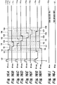
- the transfer pulse signals ⁇ V1A , ⁇ V2 , ⁇ V3A , ⁇ V4A , ⁇ V1B , ⁇ V2B , ⁇ V3B , ⁇ V2B , ⁇ V3B and ⁇ V4B are V H , V M , V H , V M , V H , V M , V H and V L , respectively, as shown in Figs. 16A through 16H.
- the signal charges Q A , Q B , Q C , Q D , Q E , Q F , Q G and Q H are read out to the vertical shift register 2.
- the transfer pulse signals ⁇ V1A , ⁇ V2 , ⁇ V3A , ⁇ V4 , ⁇ V1B , ⁇ V2 , ⁇ V3B , ⁇ V2 , ⁇ V3B and ⁇ V4 are V M , V M , V M , V M , V M , V M and V L , respectively, as shown in Figs. 16A through 16H.
- the potential wells are deep as shaded at time t2 in Fig.
- the charges Q A , Q B , Q C and Q D are combined to generate a signal charge Q A + Q B + Q C + Q D in the vertical shift register 2, and the charges Q E , Q F , Q G and Q H are combined to generate a signal charge Q E + Q F + Q G + Q H .
- the transfer pulse signals ⁇ V1A , ⁇ V2A , ⁇ V3A , ⁇ V4A , ⁇ V1B , ⁇ V2B , ⁇ V3B , ⁇ V2B , ⁇ V3B and ⁇ V4B are V M , V M , V M , V M , V M , V L and V L , respectively, as shown in Figs. 16A through 16H.
- the potential wells are deep as shaded at time t3 in Fig. 17.
- the transfer pulse signals ⁇ V1A , ⁇ V2A , ⁇ V3A , ⁇ V4A , ⁇ V1B , ⁇ V2B , ⁇ V3B , ⁇ V2B , ⁇ V3B and ⁇ V4B are V M , V M , V M , V M , V M , V M and V L , respectively, as shown in Figs. 16A through 16H.
- the potential wells are deep as shaded at time t4 in Fig. 17.
- the transfer pulse signals ⁇ V1A , ⁇ V2 , ⁇ V3A , ⁇ V4A , ⁇ V1B , ⁇ V2B , ⁇ V3B , ⁇ V2B , ⁇ V3B and ⁇ V4B are V L , V M , V M , V M , V M , V M and V L , respectively, as shown in Figs. 16A through 16H.
- the potential wells are deep as shaded at time t5 in Fig. 17.
- the vertical shift register 2 performs a one-pixel vertical shift operation upon the signal charge Q A + Q B + Q C + Q D , the signal charge Q E + Q F + Q G + Q H , ⁇ .
- the transfer pulse signals ⁇ V1A , ⁇ V2A , ⁇ V3A , ⁇ V4A , ⁇ V1B , ⁇ V2B , ⁇ V3B and ⁇ V4B are changed to times t6 and t7, time t8 and t9, times t10 and t11, times t12 and t13, times t14 and t15, t16 and t17, and times t18 and t19, in a similar way to times t4 and t5.
- the signal charge Q A + Q B + Q C + Q D is completely transferred to the horizontal output register 3.
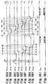
- the transfer pulse signals ⁇ V1A , ⁇ V2 , ⁇ V3A , ⁇ V4A , ⁇ V1B , ⁇ V2B , ⁇ V3B , ⁇ V2B , ⁇ V3B and ⁇ V4B are V H , V M , V H , V L , V H , V M , V H and V M , respectively, as shown in Figs. 18A through 18H.
- the signal charges Q A , Q B , Q C , Q D , Q E , Q F , Q G and Q H are read out to the vertical shift register 2.
- the transfer pulse signals ⁇ V1A , ⁇ V2A , ⁇ V3A , ⁇ V4A , ⁇ V1B , ⁇ V2B , ⁇ V3B , ⁇ V2B , ⁇ V3B and ⁇ V4B are V M , V M , V L , V L , V M , V M , V M and V M , respectively, as shown in Figs. 18A through 18H.
- the potential wells are deep as shaded at time t3 in Fig. 19.
- the transfer pulse signals ⁇ V1A , ⁇ V2A , ⁇ V3A , ⁇ V4A , ⁇ V1B , ⁇ V2B , ⁇ V3B , ⁇ V2B , ⁇ V3B and ⁇ V4B are V M , V M , V L , V M , V M , V M , V M and V M , respectively, as shown in Figs. 18A through 18H.
- the potential wells are deep as shaded at time t4 in Fig. 19.
- the transfer pulse signals ⁇ V1A , ⁇ V2 , ⁇ V3A , ⁇ V4A , ⁇ V1B , ⁇ V2B , ⁇ V3B , ⁇ V2B , ⁇ V3B and ⁇ V4B are V M , V M , V M , V L , V L , V M , V M and V M , respectively, as shown in Figs. 18A through 18H.
- the potential wells are deep as shaded at time t5 in Fig. 19.
- the vertical shift register 2 performs a one-pixel vertical shift operation upon the signal charge Q A + Q B , the signal charge Q L + Q D + Q E + Q F , ⁇ .
- the transfer pulse signals ⁇ V1A , ⁇ V2A , ⁇ V3A , ⁇ V4A , ⁇ V1B , ⁇ V2B , ⁇ V3B and ⁇ V4B are changed to times t6 and t7, time t8 and t9, and times t10, in a similar way to times t4 and t5.
- the signal charge Q A + Q B is completely transferred to the horizontal output register 3.
- the transfer pulse signals ⁇ V1A , ⁇ V2A , ⁇ V3A , ⁇ V4A , ⁇ V1B , ⁇ V2B , ⁇ V3B and ⁇ V4B are changed at times t12 and t13, t14 and t15, t16 and t17, t18 and t19, t20 and t21, t22 and t23, t24 and t25, and t26 and t27, in a similar way to times t4 and t5.
- the signal charge Q C + Q D + Q E + Q F is completely transferred to the horizontal output register 3.
- the horizontal output register 3 is designed to process every four rows of the photo/electro conversion portions 1, in other words, the width of the horizontal output register 3 is twice as compared with the prior art.
- the ratio of a width W to a length L of the transfer electrodes 8 and 9 can be twice as compared with the prior art. Therefore, the electric field within the vertical shift registers 2 along the vertical shift direction can be twice as compared with the prior art, and accordingly, the efficiency of charge transfer can be enhanced.
- the signal charge such as Q A + Q B + Q C + Q D is stored in the potential wells beneath four transfer electrodes within the vertical shift register 2 during a vertical shift operation.
- the signal charge such as Q A + Q B + Q C + Q D are stored in the potential wells beneath six or seven transfer electrodes within the vertical shift register 2 during a vertical shift operation. Therefore, the amount of the signal charge in the second embodiment can be about one and half times as large as the amount of the signal charge in the first embodiment as well as in the prior art. Therefore, in the second embodiment, the register blooming can be avoided to broaden the dynamic range.
- the ratio of width to length of the transfer electrodes of the vertical shift registers can be increased, the efficiency of charge transfer can be enhanced.
Landscapes
- Engineering & Computer Science (AREA)
- Multimedia (AREA)
- Signal Processing (AREA)
- Transforming Light Signals Into Electric Signals (AREA)
- Solid State Image Pick-Up Elements (AREA)
Applications Claiming Priority (2)
| Application Number | Priority Date | Filing Date | Title |
|---|---|---|---|
| JP133697/95 | 1995-05-31 | ||
| JP7133697A JP2865019B2 (ja) | 1995-05-31 | 1995-05-31 | 電荷転送固体撮像装置の駆動方法 |
Publications (2)
| Publication Number | Publication Date |
|---|---|
| EP0746144A2 true EP0746144A2 (de) | 1996-12-04 |
| EP0746144A3 EP0746144A3 (de) | 1998-12-23 |
Family
ID=15110775
Family Applications (1)
| Application Number | Title | Priority Date | Filing Date |
|---|---|---|---|
| EP96108795A Withdrawn EP0746144A3 (de) | 1995-05-31 | 1996-05-31 | Halbleiterbildsensor des Types CCD |
Country Status (5)
| Country | Link |
|---|---|
| US (1) | US5686742A (de) |
| EP (1) | EP0746144A3 (de) |
| JP (1) | JP2865019B2 (de) |
| KR (1) | KR100206692B1 (de) |
| TW (1) | TW305094B (de) |
Cited By (4)
| Publication number | Priority date | Publication date | Assignee | Title |
|---|---|---|---|---|
| EP0896468A3 (de) * | 1997-08-07 | 2000-05-17 | Nec Corporation | Festkörperbildaufnahmevorrichtung und Ansteuermethode dafür |
| GB2370712A (en) * | 2000-10-31 | 2002-07-03 | Hewlett Packard Co | Photosensor array with decreased scan time for decreased resolution |
| RU2187795C1 (ru) * | 2001-06-15 | 2002-08-20 | Ярославский государственный технический университет | Устройство для определения коэффициента газопроницаемости порошков |
| EP1063844A4 (de) * | 1998-02-10 | 2007-07-11 | Nikon Corp | Verfahren und steuerung eines festkörperbildgerätes, bildgerät, ausrichtungsgerät und ausrichtungsverfahren |
Families Citing this family (11)
| Publication number | Priority date | Publication date | Assignee | Title |
|---|---|---|---|---|
| JP3887878B2 (ja) * | 1997-06-03 | 2007-02-28 | ソニー株式会社 | 固体撮像素子の暗信号レベル測定方法及び測定装置 |
| JPH11164205A (ja) * | 1997-11-28 | 1999-06-18 | Sony Corp | 固体撮像装置およびその駆動方法 |
| JP3302927B2 (ja) * | 1998-07-03 | 2002-07-15 | 日本電気株式会社 | 固体撮像装置及びその駆動方法 |
| KR100606408B1 (ko) * | 1998-12-12 | 2006-11-30 | 엘지.필립스 엘시디 주식회사 | 이미지촬영장치 |
| KR100570961B1 (ko) * | 1998-12-12 | 2006-08-30 | 엘지.필립스 엘시디 주식회사 | 이미지촬영장치 |
| JP3967500B2 (ja) * | 1999-09-08 | 2007-08-29 | 富士フイルム株式会社 | 固体撮像装置および信号読出し方法 |
| JP4294810B2 (ja) * | 1999-09-10 | 2009-07-15 | 富士フイルム株式会社 | 固体撮像装置および信号読出し方法 |
| JP2001111026A (ja) * | 1999-10-07 | 2001-04-20 | Fuji Film Microdevices Co Ltd | 固体撮像装置 |
| JP5133293B2 (ja) * | 2009-04-13 | 2013-01-30 | ソニー株式会社 | 固体撮像装置およびその駆動方法並びにカメラシステム |
| JP5133292B2 (ja) * | 2009-04-13 | 2013-01-30 | ソニー株式会社 | 固体撮像装置およびその駆動方法並びにカメラシステム |
| JP5126385B2 (ja) * | 2011-05-02 | 2013-01-23 | ソニー株式会社 | 固体撮像装置およびその駆動方法並びにカメラシステム |
Family Cites Families (5)
| Publication number | Priority date | Publication date | Assignee | Title |
|---|---|---|---|---|
| US4803710A (en) * | 1986-01-09 | 1989-02-07 | General Electric Company | Storage registers with charge packet accumulation capability, as for solid-state imagers |
| JP2853216B2 (ja) * | 1989-11-09 | 1999-02-03 | 日本電気株式会社 | 固体撮像装置 |
| JP2614129B2 (ja) * | 1990-02-16 | 1997-05-28 | 富士写真フイルム株式会社 | 電子スチルカメラ |
| US5396121A (en) * | 1992-10-21 | 1995-03-07 | Sharp Kabushiki Kaisha | Solid-state imaging device and a method for driving the same |
| DE69330617T2 (de) * | 1992-11-20 | 2001-11-29 | Matsushita Electronics Corp., Takatsuki | Festkörper-Bildsensor |
-
1995
- 1995-05-31 JP JP7133697A patent/JP2865019B2/ja not_active Expired - Fee Related
-
1996
- 1996-05-31 US US08/656,470 patent/US5686742A/en not_active Expired - Fee Related
- 1996-05-31 EP EP96108795A patent/EP0746144A3/de not_active Withdrawn
- 1996-05-31 KR KR1019960019042A patent/KR100206692B1/ko not_active Expired - Fee Related
- 1996-06-05 TW TW085106818A patent/TW305094B/zh active
Cited By (9)
| Publication number | Priority date | Publication date | Assignee | Title |
|---|---|---|---|---|
| EP0896468A3 (de) * | 1997-08-07 | 2000-05-17 | Nec Corporation | Festkörperbildaufnahmevorrichtung und Ansteuermethode dafür |
| US6185270B1 (en) | 1997-08-07 | 2001-02-06 | Nec Corporation | Solid state imaging device and method for driving the same |
| CN1133317C (zh) * | 1997-08-07 | 2003-12-31 | 恩益禧电子股份有限公司 | 固态成象器件及其驱动方法 |
| EP1063844A4 (de) * | 1998-02-10 | 2007-07-11 | Nikon Corp | Verfahren und steuerung eines festkörperbildgerätes, bildgerät, ausrichtungsgerät und ausrichtungsverfahren |
| GB2370712A (en) * | 2000-10-31 | 2002-07-03 | Hewlett Packard Co | Photosensor array with decreased scan time for decreased resolution |
| US6765699B1 (en) | 2000-10-31 | 2004-07-20 | Hewlett-Packard Development Company, L.P. | Photosensor array with decreased scan time for decreased optical sampling rates |
| GB2370712B (en) * | 2000-10-31 | 2004-08-25 | Hewlett Packard Co | Photosensor array with decreased scan time for decreased optical sampling rates |
| US6791726B2 (en) | 2000-10-31 | 2004-09-14 | Hewlett-Packard Development Company, L.P. | Photosensor array with decreased scan time for decreased optical sampling rates |
| RU2187795C1 (ru) * | 2001-06-15 | 2002-08-20 | Ярославский государственный технический университет | Устройство для определения коэффициента газопроницаемости порошков |
Also Published As
| Publication number | Publication date |
|---|---|
| US5686742A (en) | 1997-11-11 |
| KR960043789A (ko) | 1996-12-23 |
| JPH08330563A (ja) | 1996-12-13 |
| KR100206692B1 (ko) | 1999-07-01 |
| JP2865019B2 (ja) | 1999-03-08 |
| EP0746144A3 (de) | 1998-12-23 |
| TW305094B (de) | 1997-05-11 |
Similar Documents
| Publication | Publication Date | Title |
|---|---|---|
| US5686742A (en) | CCD type solid state image pickup device having high charge transfer efficiency | |
| US6075565A (en) | Solid-state image sensing apparatus and its driving method | |
| US7944495B2 (en) | Solid-state image pickup element including a thinning method to discharge unnecessary image data | |
| EP0313322B1 (de) | Halbleiterbildsensor mit mehrfachen horizontalen Transferabschnitten | |
| EP0812114A1 (de) | Festkörper-bildaufnahmevorrichtung,verfahren zur ansteuerung und festkörperkamera und kamerasystem | |
| JPH0529192B2 (de) | ||
| JPS5984575A (ja) | 固体撮像素子 | |
| KR890005237B1 (ko) | 고체촬상소자 및 그 구동방법 | |
| US4675887A (en) | Solid state imaging device and method with row-by-row charge transfer | |
| EP0869665B1 (de) | Festkörper-Bildsensor | |
| JPH05199465A (ja) | 電荷結合撮像デバイスとそのような撮像デバイスを備えるカメラ | |
| KR20080069119A (ko) | 고체 촬상 장치 | |
| JPS62208668A (ja) | 電荷移送形固体撮像素子 | |
| US6355949B1 (en) | Solid state imaging apparatus with horizontal charge transfer register which can transfer signal charge faster | |
| JP4419275B2 (ja) | 固体撮像装置およびその駆動方法並びに画像入力装置 | |
| JPH09205192A (ja) | 電荷結合素子形固体撮像素子とその製造及び駆動方法 | |
| JPH07322143A (ja) | 固体撮像装置の駆動方法 | |
| JP3036250B2 (ja) | Ccd素子 | |
| JP2623150B2 (ja) | 固体撮像デバイス | |
| JPH0514816A (ja) | 固体撮像装置およびその駆動方法 | |
| JP2993492B2 (ja) | 固体撮像装置の駆動方法及び駆動装置 | |
| JPS6046594B2 (ja) | 電荷転送撮像素子の駆動方法 | |
| JP2001094740A (ja) | 固体撮像装置およびその駆動方法並びに画像入力装置 | |
| JP3008629B2 (ja) | 固体撮像素子 | |
| JPH09129861A (ja) | 固体撮像素子 |
Legal Events
| Date | Code | Title | Description |
|---|---|---|---|
| PUAI | Public reference made under article 153(3) epc to a published international application that has entered the european phase |
Free format text: ORIGINAL CODE: 0009012 |
|
| AK | Designated contracting states |
Kind code of ref document: A2 Designated state(s): DE FR GB |
|
| PUAL | Search report despatched |
Free format text: ORIGINAL CODE: 0009013 |
|
| AK | Designated contracting states |
Kind code of ref document: A3 Designated state(s): DE FR GB |
|
| 17P | Request for examination filed |
Effective date: 19990301 |
|
| 17Q | First examination report despatched |
Effective date: 20021021 |
|
| RAP1 | Party data changed (applicant data changed or rights of an application transferred) |
Owner name: NEC ELECTRONICS CORPORATION |
|
| GRAP | Despatch of communication of intention to grant a patent |
Free format text: ORIGINAL CODE: EPIDOSNIGR1 |
|
| STAA | Information on the status of an ep patent application or granted ep patent |
Free format text: STATUS: THE APPLICATION HAS BEEN WITHDRAWN |
|
| 18W | Application withdrawn |
Effective date: 20031204 |