EP0746155A2 - Mehrnormen-Fernsehempfänger - Google Patents
Mehrnormen-Fernsehempfänger Download PDFInfo
- Publication number
- EP0746155A2 EP0746155A2 EP96304001A EP96304001A EP0746155A2 EP 0746155 A2 EP0746155 A2 EP 0746155A2 EP 96304001 A EP96304001 A EP 96304001A EP 96304001 A EP96304001 A EP 96304001A EP 0746155 A2 EP0746155 A2 EP 0746155A2
- Authority
- EP
- European Patent Office
- Prior art keywords
- video signal
- signal processing
- selection control
- output terminals
- selection
- Prior art date
- Legal status (The legal status is an assumption and is not a legal conclusion. Google has not performed a legal analysis and makes no representation as to the accuracy of the status listed.)
- Granted
Links
Images



Classifications
-
- H—ELECTRICITY
- H04—ELECTRIC COMMUNICATION TECHNIQUE
- H04N—PICTORIAL COMMUNICATION, e.g. TELEVISION
- H04N5/00—Details of television systems
- H04N5/44—Receiver circuitry for the reception of television signals according to analogue transmission standards
- H04N5/46—Receiver circuitry for the reception of television signals according to analogue transmission standards for receiving on more than one standard at will
-
- H—ELECTRICITY
- H04—ELECTRIC COMMUNICATION TECHNIQUE
- H04N—PICTORIAL COMMUNICATION, e.g. TELEVISION
- H04N5/00—Details of television systems
- H04N5/04—Synchronising
- H04N5/08—Separation of synchronising signals from picture signals
-
- H—ELECTRICITY
- H04—ELECTRIC COMMUNICATION TECHNIQUE
- H04N—PICTORIAL COMMUNICATION, e.g. TELEVISION
- H04N5/00—Details of television systems
- H04N5/76—Television signal recording
- H04N5/765—Interface circuits between an apparatus for recording and another apparatus
- H04N5/775—Interface circuits between an apparatus for recording and another apparatus between a recording apparatus and a television receiver
Definitions
- the present invention relates to a television receiver which decodes video signals for a plurality of broadcast standards, such as MUSE (multiple sub-Nyquist sampling encoding) standard to transmit a HighVision signal and EDTV-2 (second generation extended definition television) standard.
- MUSE multiple sub-Nyquist sampling encoding
- EDTV-2 second generation extended definition television
- a decoder for a MUSE standard is introduced in a technical report "MUSE HighVision transmission standard” by Ninomiya edited by Electronic Information Communication Institute and a decoder for an EDTV-2 standard is introduced in "Part 2, transmission and reception circuits -- high resolution component is separately transmitted", Nikkei Electronics 1994, January 31 vol. 600, pp.142-149.
- FIGs. 8 and 9 Examples of a block diagram generally thought as a decoder part of a television receiver which can receive a plurality of kinds of broadcast standards are shown in FIGs. 8 and 9.
- a case having two video signal processing blocks as a plurality of video signal processing means and three channels for each MUSE standard and NTSC standard as the number of video signal sources is described for simplicity of explanation.
- FIG. 8 is an example of a block diagram of a decoder part of a television receiver for receiving multi-standards to be generally thought in accordance with the prior art.
- the terminals 1, 2 and 3 are video signal input terminals for a MUSE standard signal.
- the block 4 is a selector circuit for selecting a video signal out of a plurality of input terminals 1, 2 and 3.
- the block 5 is an A/D (from analog to digital) converter for converting an analog video signal oitputted from selector circuit 4 into a digital video signal.
- the block 6 is a first video signal processing block for decoding an output signal of A/D converter 5.
- the block 120 is a first memory block for storing a video signal during several frame periods and is connected to first video signal processing block 6.
- the block 126 is a D/A (from digital to analog) converter for converting a digital video signal outputted from first video signal processing block 6 into an analog video signal.
- the terminals 11, 12 and 13 are video signal input terminals for an EDTV-2 standard signal.
- the block 14 is a selector circuit for selecting a video signal out of a plurality of input terminals 11, 12 and 13.
- the block 15 is an A/D converter for converting an analog output signal of selector circuit 14 into a digital signal.
- the block 16 is a second video signal processing block for decoding an output signal of A/D converter 15.
- the block 220 is a second memory block for storing a video signal during several frame periods and is connected to second video signal processing block 16.
- the block 226 is a D/A converter for converting an output signal of second video signal processing block 16 into an analog signal.
- the block 25 is a selector circuit for selecting an output signal of either D/A converter 126 or 226.
- the terminal 27 is an output terminal of selector circuit 25.
- the block 21 is a selection control circuit for controlling selection of selection circuits 4, 14 and 25.
- a selection control circuit 21 controls selector circuit 25 so as to select an output of D/A converter 126 and selects an input signal by controlling a selector circuit 4. For example, when a satellite broadcast (BS, hereafter) is received, an input terminal 1 connected to a detector output terminal of a BS tuner is selected and when a laser disk picture is watched, an input terminal 2 connected to an external input terminal is selected.
- BS satellite broadcast
- the inputted video signal is decoded at a first video signal processing block 6 after being converted into a digital signal at an A/D converter 5.
- the first video signal processing block 6 is composed of a moving picture processing block for executing interpolation processing from an input signal during continuous several horizontal-scanning periods, a still picture processing block for executing interpolation processing from a signal during two frame periods stored in first memory block 120, a movement detecting block for detecting a moving part from the signal during the two frame periods and a block for mixing an output signal of the moving picture processing block and an output signal of the still picture processing block and outputs a signal in which its mixing ratio is varied according to a signal expressing a degree of movement supplied from the movement detecting block.
- a video signal of MUSE system is decoded.
- selection control circuit 21 controls selector circuit 25 so as to select an output of D/A converter 226 and selects an input signal by controlling selector circuit 14. For example, when an EDTV-2 broadcast is received, an input terminal 11 connected to a detector output terminal of a tuner is selected and when a laser disk picture or a video cassette picture is watched, input terminal 12 connected to an external input terminal is selected.
- the inputted video signal is decoded at second video signal processing block 16 after being converted into a digital signal at A/D converter 15.
- a composite video signal is separated into a luminance signal and a chrominance signal (that is, Y/C separation) by three dimensional processing and an enhanced signal multiplexed on the luminance signal is decoded and reproduced to increase vertical and horizontal resolution are increased.
- a high frequency component to be superimposed is controlled by a movement signal detected from a frame difference signal.
- a video signal of EDTV-2 standard is decoded.
- memory blocks 120 and 220 are used for a MUSE standard signal and an EDTV-2 standard signal, respectively and the memory block is not used in common.
- FIG. 9 is another example of a block diagram of a decoder part of a television receiver for receiving multi-standards to be generally thought in accordance with the prior art.
- the terminals 1, 2 and 3 are video signal input terminals for MUSE standard.
- the block 4 is a selector circuit for selecting a video signal out of a plurality of input terminals 1, 2 and 3.
- the block 5 is an A/D converter for converting an analog output signal of selector circuit 4 into a digital signal.
- the block 6 is a first video signal processing block for decoding an output signal of A/D converter 5.
- the block 126 is a D/A converter for converting an output signal of first video signal processing block 6 into an analog signal.
- the terminals 11, 12 and 13 are video signal input terminals for EDTV-2 standard.
- the block 14 is a selector circuit for selecting a video signal out of a plurality of input terminals 11, 12 and 13.
- the block 15 is an A/D converter for converting an analog output signal of selector circuit 14 into a digital signal.
- the block 16 is a second video signal processing block for decoding an output signal of A/D converter 15.
- the block 226 is a D/A converter for converting an output signal of second video signal processing block 16 into an analog signal.
- the block 25 is a selector circuit for selecting an output signal of either D/A converter 126 or 226.
- the block 20 is a memory block for storing a video signal during several frame periods and is connected to first video signal processing block 6.
- the block 23 is a tristate buffer through which an output signal of first video signal processing block 6 is supplied to memory block 20.
- the block 24 is a tristate buffer through which an output signal of second video signal processing block 16 is supplied to memory block 20.
- the block 21 is a selection control circuit for controlling selection of selection circuits 4, 14 and 25 and tristate buffers 23 and 24.
- the basic function is similar to that of the previous example shown in FIG. 8.
- the difference from that shown in FIG. 8 is that a memory block 20 used at video signal decoding of each standards is used in common and this point is an improved point from the previous example.
- tristate buffer 23 is controlled to be in a normal output state and tristate buffer 24 is controlled so as to be in a high impedance state. This control is made by an output signal of selection control circuit 21.
- tristate buffer 23 is controlled to be in a high impedance state and tristate buffer 24 is controlled si as to be in a normal output state.
- the first object of the present invention is that a selection drive of a plurality of video signal processing blocks is made to be optimum and not to break driving elements in a television receiver having a plurality of video signal processing blocks using one memory block in common.
- the second object of the present invention is to present a television receiver in which wasteful power dissipation is decreased at switching of a plurality of video signal processing blocks and it takes only short time to output a video signal even when a drive clock signal to the video-signal processing block which is not used for decreasing power dissipation is stopped.
- a television receiver for receiving multi-standards in accordance with a first exemplary embodiment of the present invention comprises:
- a second exemplary embodiment of the present invention is configured so that power supplies of the circuits in each video signal processing block which is in an unused state excluding a sync separator circuit can be stopped according to a control signal of the video signal processing selection circuit.
- a third exemplary embodiment of the present invention comprises a drive clock signal generator circuit which can stop a drive clock signal of the video signal processing blocks excluding a sync separator circuit according to a control signal of the video signal processing selection circuit.
- the second selection control circuit includes:
- the second selection control circuit is connected to the output terminals of the sync detection circuits and the first selection control circuit and provides with a judgment circuit for independently controlling the tristate functions of the video signal processing blocks.
- a television receiver for receiving multi-standards having a memory block in common without breaking drive elements at the output terminals of the video signal processing blocks to the memory blocks and without dissipating wasteful power can be realized. It is possible to shorten the time for outputting a video signal when a video signal processing block is selected, attempting to reduce the power consumption at the video signal processing blocks which are in an unused state.
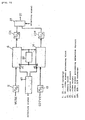
- FIG. 1 is a block diagram of a decoder part of a television receiver for receiving multi-standards in accordance with a first exemplary embodiment of the present invention.
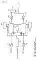
- FIG. 2 is a block diagram of a decoder part of a television receiver for receiving multi-standards in accordance with a second exemplary embodiment of the present-invention.
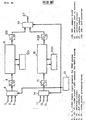
- FIG. 3 is a block diagram of a decoder part of a television receiver for receiving multi-standards in accordance with a third exemplary embodiment of the present invention.
- FIG. 4 is a block diagram of a decoder part of a television receiver for receiving multi-standards in accordance with a fourth exemplary embodiment of the present invention.
- FIG. 5 is a block diagram of a second selection control circuit of a decoder part of a television receiver for receiving multi-standards in accordance with a fifth exemplary embodiment of the present invention.
- FIG. 6 is a block diagram of an expansion circuit used in the fifth exemplary embodiment of the present invention and a timing chart.
- FIG. 7 is a block diagram of a second selection control circuit of a decoder part of a television receiver for receiving multi-standards in accordance with a sixth exemplary embodiment of the present invention.
- FIG. 8 is an example of a block diagram of a decoder part of a television receiver for receiving multi-standards in accordance with the prior art.
- FIG. 9 is another example of a block diagram of a decoder part of a television receiver for receiving multi-standards in accordance with the prior art.
- FIG. 1 is a block diagram of a decoder part of a television receiver for receiving multi-standards in accordance with a first exemplary embodiment of the present invention.
- A/D converters 5 and 15 convert analog video signals of MUSE and EDTV-2 standards, respectively to digital video signals.
- Video signal processing blocks 6 and 16 process the digital video signals of MUSE and EDTV-2 standards, respectively.
- a memory block 20 is used as a memory for processing a video signal of either MUSE or EDTV-2 standard processed at video signal processing blocks 6 and 16, respectively and selected by a signal from a video signal processing selection circuit 40.
- Video signal processing selection circuit 40 makes the output terminal of video signal processing blocks excluding the video signal processing block selected by a selection signal to the memory block a high impedance state.
- D/A converters 126 and 226 convert the digital video signals processed at video signal processing blocks 6 and 16 into analog video signals.
- a selector circuit 25 selects and outputs an output signal of either video signal processing blocks 6 or 16 by selection signals.
- the output terminals of both video signal processing blocks to memory block 20 are once made high impedance state by two independent control signal lines from video signal processing selection circuit 40 and then only the output terminal of the video signal processing block to be selected to memory block 20 is released from a high impedance state and controlled to be in a normal output state.
- the first exemplary embodiment of the present invention because there is no period during which a plurality of video signal processing blocks are simultaneously in an output state, there is no danger that a signal at one of the output terminals flows into the other output terminal due to a drive ability difference between the output terminals and a drive element at the other output terminal is broken.
- FIG. 2 is a block diagram of a decoder part of a television receiver for receiving multi-standards in accordance with a second exemplary embodiment of the present invention.
- A/D converters 5 and 15, video signal processing blocks 6 and 16, a memory block 20, a video signal processing selection circuit 40, D/A converters 126 and 226 and a selector circuit 25 are similar to those in the first exemplary embodiment of the present invention and their descriptions are omitted.
- the blocks 128 and 228 are power supplies, each has an independent power supply switch and supplies power to its corresponding video signal processing block.
- Video signal processing selection circuit 40 is connected to power supply switches of power supply circuits 128 and 228 by control signal lines and controls not to supply power to the video signal processing block which is in an unused state.
- the second exemplary embodiment of the present invention in addition to the effect mentioned in the first exemplary embodiment, it is possible to decrease power consumption although the time necessary for starting outputting a video signal at selecting a video signal processing block is less shortened.
- FIG. 3 is a block diagram of a decoder part of a television receiver for receiving multi-standards in accordance with a third exemplary embodiment of the present invention.
- A/D converters 5 and 15, video signal processing blocks 6 and 16, a memory block 20, a video signal processing selection circuit 40, D/A converters 126 and 226 and a selector circuit 25 are similar to those in the first exemplary embodiment of the present invention and their descriptions are omitted.
- the blocks 127 and 227 are sync separator circuits and separate sync signals from a MUSE signal and a EDTV-2 signal, respectively.
- the blocks 129 and 229 are driving clock signal generators for supplying driving clock signals necessary for a MUSE signal and a EDTV-2 signal, respectively.
- Video signal processing selection circuit 40 is connected to driving clock signal generators 129 and 229 by control signal lines.
- Driving clock signal generators 129 and 229 always supply driving clock signals to sync separator circuits 127 and 227.
- a driving clock signal is supplied to only a video signal processing block to be used and is not supplied to the other video signal processing block by a control signal from video signal processing selection circuit 40.
- the third exemplary embodiment of the present invention in addition to the effect mentioned in the first exemplary embodiment, it is possible to decrease power consumption by stopping a driving clock signal to a video signal processing block which is in an unused state and it is possible to select a video signal processing block faster by making always supplying driving clock signals to the sync separator circuits.
- FIG. 4 is a block diagram of a decoder part of a television receiver for receiving multi-standards in accordance with a fourth exemplary embodiment of the present invention.
- the terminals 1, 2 and 3 are video signal input terminals for MUSE standard.
- the block 4 is a selector circuit for selecting a video signal out of a plurality of input terminals 1, 2 and 3.
- the block 5 is an A/D converter for converting an analog output signal of selector circuit 4 into a digital signal.
- the block 6 is a first video signal processing block for decoding an output signal of A/D converter 5.
- the terminals 11, 12 and 13 are video signal input terminals for EDTV-2 standard.
- the block 14 is a selector circuit for selecting a video signal out of a plurality of input terminals 11, 12 and 13.
- the block 15 is an A/D converter for converting an analog output signal of selector circuit 14 into a digital signal.
- the block 16 is a second video signal processing block for decoding an output signal of A/D converter 15.
- the block 20 is a memory block for storing a video signal during several frame periods and is connected to video signal processing blocks 6 and 16.
- the blocks 23 and 24 are tristate buffers inserted at the output terminals of video signal processing blocks 6 and 16 to memory block 20, respectively.
- the block 25 is a selector circuit for selecting an output signal of either video signal processing block 6 or 16.
- the block 26 is a D/A converter for converting a digital output signal of selector circuit 25 into an analog signal.
- the block 7 is a first sync detection circuit for detecting if a sync signal of MUSE standard is included in the output signal of A/D converter 5.
- the block 17 is a second sync detection circuit for detecting if a sync signal of NTSC standard is included in the output signal of A/D converter 15.
- the block 21 is a first selection control circuit for controlling first selector circuit 4, second selector circuit 14 and second selection control circuit 22.
- the block 22 is a second selection control circuit connected to the output terminals of first sync detection circuit 7, second sync detection circuit 17 and first selection control circuit 21 and controls tristate buffers 23 and 24 and output selector circuit 25.
- First sync detection circuit 7 detects a frame pulse forming a MUSE standard and outputs a signal "sync yes” if a sync signal is detected and outputs a signal "sync no” if a sync signal is not detected.
- second sync detection circuit 17 detects a vertical sync signal of an NTSC standard and outputs.
- first selection control circuit 21 controls selector circuits 4 and 14 so as to select input terminals 1 and 11 connected to the output terminals of the BS tuner.
- tristate buffer 23 When a sync signal of MUSE standard is detected at first sync detection circuit 7, tristate buffer 23 is made a normal output state by an output signal of second selection control circuit 22 and tristate buffer 24 is made a high impedance state and selector circuit 25 is controlled so as to select an output signal of first video signal processing block 6.
- selector circuit 25 is controlled so as to select an output signal of first video signal processing block 6.
- tristate buffer 23 When a sync signal of MUSE standard is not detected at first sync detection circuit 7, tristate buffer 23 is made a high impedance state by the output of first sync detection circuit 7 and tristate buffer 24 is made a normal output state and selector circuit 25 is controlled so as to select an output signal of second video signal processing block 16.
- a video signal of NTSC standard is processed using memory block 20 together with second video signal processing_block 16.
- video signal processing there are decoding of an EDTV-2 signal, two pictures on the same screen, stopping a picture and so on.
- selector 14 selects input terminal 12 connected to an external input terminal by the output signal of first selection control circuit 21.
- selector circuit 4 selects input terminal 1 connected to the output terminal of the BS tuner and a sync signal of MUSE standard is detected at first sync detection circuit 7, second selection control circuit 22 controls tristate buffers 23 and 24 only using the output of first selection control circuit 21 and without using the output of first sync detection circuit 7.
- first sync detection circuit 7 is used was described above, it is also possible to control using second sync detection circuit 17.
- the fourth exemplary embodiment of the present invention it is possible to control selection correctly with a memory block in common by providing a plurality of video signal sync detection circuits, first selection control circuit for selecting input/output video signals and second selection control circuit connected to the output terminals of the sync detection circuits and the first selector circuit and controls tristate functions of the video signal processing blocks, even if a plurality of standards such as MUSE standard and EDTV-2 standard are broadcast on the same channel.
- FIG. 5 is a block diagram of a second selection control circuit of a decoder part of a television receiver for receiving multi-standards in accordance with a fifth exemplary embodiment of the present invention.
- the block 221 is an expansion circuit connected to output terminal A of first sync detection circuit 7 shown in FIG. 4.
- the block 222 is a judgment circuit connected to output terminal Z of expansion circuit 221 and output terminal C of first selection control circuit 21 shown in FIG. 4.
- the block 223 is a reversing circuit for reversing a polarity of the output of judgment circuit 222.
- FIG. 6 is a block diagram of expansion circuit 221 used in the fifth exemplary embodiment of the present invention and a timing chart explaining its function.
- judgment circuit 222 functions so as to control tristate buffer 23 and 24 by the output signal from sync detection circuit 7 or 17.
- judgment circuit 222 functions so as to control tristate buffer 23 and 24 by the output signal from first selection control circuit 21.
- expansion circuit 221 is delayed (about 4 frame periods) until the next sync signal is detected.
- the output signal of expansion circuit 221 does not vary. For example, as shown in FIG. 6, after sync detection, if a sync signal is detected, the signal level is made low and if no sync signal is detected, the signal level is made high. If a signal A inputted to expansion circuit 221 and a signal Y delayed by several frame periods are inputted to an AND circuit, a desired signal Z is outputted from the AND circuit.
- first sync detection circuit 7 of MUSE standard is described in the above explanation, also the case of second sync detection circuit 17 is similar.
- FIG. 7 is a block diagram of another example of a second selection control circuit of a decoder part of a television receiver for receiving multi-standards in accordance with a sixth exemplary embodiment of the present invention.
- the block 224 is a judgment circuit connected to the output terminal A of first sync detection circuit 7, the output terminal B of second sync detection circuit 17 and the output terminal C of first selection control circuit 21.
- the basic function is similar to those of the fourth and fifth exemplary embodiments of the present invention. Let's consider a case in which there are a plurality of signals having different broadcast standards in the same channel. For example, the case in which both input selector circuits 4 and 14 select input terminals 1 and 11 connected to the output terminal of a BS tuner by first selection control circuit 21. In this case, it does not occur that both sync detection circuits 7 and 17 output signals indicating "sync yes" in the same time.
- judgment circuit 224 controls tristate buffer 23 at the output terminal of first video signal processing block 6 on the basis of the output signals of first sync detection circuit 7 and first selection control circuit 21 and controls tristate buffer 24 of second video signal processing block 16 on the basis of the output signals of second sync detection circuit 17 and first selection control circuit 21.
- the sixth exemplary embodiment of the present invention by providing a judgment circuit connected to the output terminals of a plurality of sync detection circuits and a first selection control circuit and for independently controlling tristate buffers of a plurality of video signal processing blocks, it is possible to correctly and quickly select a signal to be stored in a common memory block, even if there are a plurality of broadcast standards in the same channel.
Landscapes
- Engineering & Computer Science (AREA)
- Multimedia (AREA)
- Signal Processing (AREA)
- Television Systems (AREA)
- Picture Signal Circuits (AREA)
- Circuits Of Receivers In General (AREA)
- Television Receiver Circuits (AREA)
Applications Claiming Priority (4)
| Application Number | Priority Date | Filing Date | Title |
|---|---|---|---|
| JP136468/95 | 1995-06-02 | ||
| JP7136468A JPH08331478A (ja) | 1995-06-02 | 1995-06-02 | テレビジョン受像機 |
| JP13766595A JP3228072B2 (ja) | 1995-06-05 | 1995-06-05 | テレビジョン受像機 |
| JP137665/95 | 1995-06-05 |
Publications (3)
| Publication Number | Publication Date |
|---|---|
| EP0746155A2 true EP0746155A2 (de) | 1996-12-04 |
| EP0746155A3 EP0746155A3 (de) | 1999-01-20 |
| EP0746155B1 EP0746155B1 (de) | 2007-08-01 |
Family
ID=26470044
Family Applications (1)
| Application Number | Title | Priority Date | Filing Date |
|---|---|---|---|
| EP96304001A Expired - Lifetime EP0746155B1 (de) | 1995-06-02 | 1996-06-03 | Mehrnormen-Fernsehempfänger |
Country Status (6)
| Country | Link |
|---|---|
| US (1) | US6137537A (de) |
| EP (1) | EP0746155B1 (de) |
| KR (1) | KR100305874B1 (de) |
| CN (1) | CN1158867C (de) |
| DE (1) | DE69637189T2 (de) |
| TW (1) | TW366658B (de) |
Cited By (1)
| Publication number | Priority date | Publication date | Assignee | Title |
|---|---|---|---|---|
| GB2337679B (en) * | 1997-02-19 | 2001-05-09 | Sanyo Electric Co | Television receiver |
Families Citing this family (16)
| Publication number | Priority date | Publication date | Assignee | Title |
|---|---|---|---|---|
| JP3703247B2 (ja) * | 1997-03-31 | 2005-10-05 | 三菱電機株式会社 | プラズマディスプレイ装置及びプラズマディスプレイ駆動方法 |
| JP3564961B2 (ja) | 1997-08-21 | 2004-09-15 | 株式会社日立製作所 | ディジタル放送受信装置 |
| JPH1188716A (ja) * | 1997-09-03 | 1999-03-30 | Hitachi Ltd | ディスプレイ装置 |
| US6353460B1 (en) * | 1997-09-30 | 2002-03-05 | Matsushita Electric Industrial Co., Ltd. | Television receiver, video signal processing device, image processing device and image processing method |
| KR100326287B1 (ko) * | 1998-03-31 | 2002-06-26 | 윤종용 | 저장된 채널정보를 이용하여 채널선택이 이루어지는 디지털tv수상기및 그방법 |
| US6341375B1 (en) * | 1999-07-14 | 2002-01-22 | Lsi Logic Corporation | Video on demand DVD system |
| JP3820891B2 (ja) * | 2001-02-07 | 2006-09-13 | セイコーエプソン株式会社 | 画像表示装置 |
| JP3744819B2 (ja) * | 2001-05-24 | 2006-02-15 | セイコーエプソン株式会社 | 信号駆動回路、表示装置、電気光学装置及び信号駆動方法 |
| US8284844B2 (en) | 2002-04-01 | 2012-10-09 | Broadcom Corporation | Video decoding system supporting multiple standards |
| JP2006511850A (ja) | 2002-04-19 | 2006-04-06 | コンピュータ アソシエイツ シンク,インコーポレイテッド | データマイニングのためのニューラルネットワークの使用 |
| WO2004084535A2 (en) * | 2003-03-14 | 2004-09-30 | Starz Encore Group Llc | Video aspect ratio manipulation |
| JP4504714B2 (ja) * | 2004-03-26 | 2010-07-14 | リーダー電子株式会社 | 外部同期信号生成回路および位相差測定回路 |
| US20060025743A1 (en) * | 2004-07-30 | 2006-02-02 | The Procter & Gamble Company | Absorbent article with color matched surfaces |
| KR100598396B1 (ko) * | 2004-10-01 | 2006-07-06 | 삼성전자주식회사 | 디스플레이장치 및 그 제어방법 |
| KR101046588B1 (ko) * | 2005-11-16 | 2011-07-06 | 삼성전자주식회사 | 신호처리장치 및 그 제어방법 |
| JP2010048976A (ja) * | 2008-08-20 | 2010-03-04 | Sony Corp | 信号処理装置および信号処理方法 |
Family Cites Families (16)
| Publication number | Priority date | Publication date | Assignee | Title |
|---|---|---|---|---|
| JPS58213586A (ja) * | 1982-06-04 | 1983-12-12 | Toshiba Corp | 位相合成装置 |
| JPS6022264A (ja) * | 1983-07-18 | 1985-02-04 | Matsushita Electric Ind Co Ltd | デ−タ処理装置 |
| JP2563338B2 (ja) * | 1987-06-02 | 1996-12-11 | 松下電器産業株式会社 | 低雑音コンバ−タ |
| JP3024133B2 (ja) * | 1988-12-06 | 2000-03-21 | 松下電器産業株式会社 | テレビジョン受像機 |
| US4962428A (en) * | 1989-04-20 | 1990-10-09 | Motorola, Inc. | Multistandard OSD in a TV receiver including display positioning |
| JPH02302184A (ja) * | 1989-05-16 | 1990-12-14 | Mitsubishi Electric Corp | 衛星放送受信機 |
| JP2779212B2 (ja) * | 1989-07-17 | 1998-07-23 | 株式会社日立製作所 | ワイド画面/標準画面テレビジョン信号受信装置 |
| JP3361143B2 (ja) * | 1993-04-09 | 2003-01-07 | 株式会社日立製作所 | テレビジョン信号処理回路及びテレビジョン信号処理装置 |
| KR0140674B1 (ko) * | 1993-04-12 | 1998-06-15 | 모리시다 요이치 | 영상신호처리장치 및 처리방법 |
| JP3527259B2 (ja) * | 1993-04-12 | 2004-05-17 | 松下電器産業株式会社 | 映像信号処理装置及び処理方法 |
| KR0142803B1 (ko) * | 1993-09-02 | 1998-07-15 | 모리시다 요이치 | 신호처리장치 |
| JPH0787526A (ja) * | 1993-09-16 | 1995-03-31 | Sony Corp | サンプリングレート変換システム |
| US5557337A (en) * | 1994-02-18 | 1996-09-17 | Hitachi America, Ltd. | Automatic television signal detector to differentiate NTSC signals from HDJV/AJV signals |
| US5374962A (en) * | 1994-03-30 | 1994-12-20 | Thomson Consumer Electronics, Inc. | Multi-standard TV receiver with luma/chroma delay compensation |
| US5461427A (en) * | 1994-06-28 | 1995-10-24 | Thomson Consumer Electronics, Inc. | Television receiver having the capability to associate any HDTV and any NTSC channel |
| US5796442A (en) * | 1994-11-02 | 1998-08-18 | Texas Instruments Incorporated | Multi-format television reciever |
-
1996
- 1996-06-01 KR KR1019960019474A patent/KR100305874B1/ko not_active Expired - Fee Related
- 1996-06-03 EP EP96304001A patent/EP0746155B1/de not_active Expired - Lifetime
- 1996-06-03 CN CNB961066954A patent/CN1158867C/zh not_active Expired - Fee Related
- 1996-06-03 DE DE69637189T patent/DE69637189T2/de not_active Expired - Fee Related
- 1996-06-22 TW TW085107534A patent/TW366658B/zh active
-
1998
- 1998-09-28 US US09/162,398 patent/US6137537A/en not_active Expired - Fee Related
Cited By (1)
| Publication number | Priority date | Publication date | Assignee | Title |
|---|---|---|---|---|
| GB2337679B (en) * | 1997-02-19 | 2001-05-09 | Sanyo Electric Co | Television receiver |
Also Published As
| Publication number | Publication date |
|---|---|
| DE69637189T2 (de) | 2007-12-20 |
| CN1139348A (zh) | 1997-01-01 |
| CN1158867C (zh) | 2004-07-21 |
| EP0746155A3 (de) | 1999-01-20 |
| KR100305874B1 (ko) | 2001-11-30 |
| DE69637189D1 (de) | 2007-09-13 |
| KR970004807A (ko) | 1997-01-29 |
| TW366658B (en) | 1999-08-11 |
| EP0746155B1 (de) | 2007-08-01 |
| US6137537A (en) | 2000-10-24 |
Similar Documents
| Publication | Publication Date | Title |
|---|---|---|
| US6137537A (en) | Television receiver for receiving multi-standards | |
| US7375761B2 (en) | Receiver having motion picture data decoder | |
| US5229855A (en) | System and method for combining multiple composite video signals | |
| US8345169B2 (en) | Signal transmitter and signal receiver | |
| US5065243A (en) | Multi-screen high-definition television receiver | |
| US5442398A (en) | Method and apparatus for transmitting a video signal, and apparatus for receiving a video signal | |
| US4931855A (en) | Method for generating and transmitting high-definition color television signals, compatible with current standards and process and apparatus for receiving said signals | |
| EP0860992B1 (de) | Fernsehempfänger mit Abtastkonverter und entsprechende Methode | |
| EP0661873B1 (de) | Videosignal Sende-Empfänger und Signalübertragungsgerät zu dessen Verwendung | |
| EP0717562A1 (de) | Verfahren und Vorrichtung zur gleichzeitigen Darstellung von zwei Bildern | |
| US5301015A (en) | NTSC and PAL compatible digital encoder | |
| JP3228072B2 (ja) | テレビジョン受像機 | |
| JP2517650B2 (ja) | 帯域圧縮テレビジョン信号の受信装置 | |
| KR100222762B1 (ko) | 문자방송 기능 지원용 병렬/직렬변환회로 | |
| JPH0514832A (ja) | テレビジヨン信号受信機 | |
| JPS61136393A (ja) | 文字多重放送受信機の自動走査切換方式 | |
| JP2001008120A (ja) | 映像合成回路 | |
| JPH07245743A (ja) | 高品位テレビジョン信号処理回路 | |
| JPH10322620A (ja) | ディジタル放送受信機 | |
| JPH02291791A (ja) | テレビジョン方式変換器 | |
| JPH0678237A (ja) | テレビジョン信号受信機 | |
| JPH05236382A (ja) | テレビジョン受像機の映像受信回路 |
Legal Events
| Date | Code | Title | Description |
|---|---|---|---|
| PUAI | Public reference made under article 153(3) epc to a published international application that has entered the european phase |
Free format text: ORIGINAL CODE: 0009012 |
|
| AK | Designated contracting states |
Kind code of ref document: A2 Designated state(s): DE FR GB |
|
| PUAL | Search report despatched |
Free format text: ORIGINAL CODE: 0009013 |
|
| AK | Designated contracting states |
Kind code of ref document: A3 Designated state(s): DE FR GB |
|
| 17P | Request for examination filed |
Effective date: 19990607 |
|
| 17Q | First examination report despatched |
Effective date: 20010309 |
|
| GRAP | Despatch of communication of intention to grant a patent |
Free format text: ORIGINAL CODE: EPIDOSNIGR1 |
|
| GRAS | Grant fee paid |
Free format text: ORIGINAL CODE: EPIDOSNIGR3 |
|
| GRAA | (expected) grant |
Free format text: ORIGINAL CODE: 0009210 |
|
| AK | Designated contracting states |
Kind code of ref document: B1 Designated state(s): DE FR GB |
|
| REG | Reference to a national code |
Ref country code: GB Ref legal event code: FG4D |
|
| REF | Corresponds to: |
Ref document number: 69637189 Country of ref document: DE Date of ref document: 20070913 Kind code of ref document: P |
|
| ET | Fr: translation filed | ||
| PLBE | No opposition filed within time limit |
Free format text: ORIGINAL CODE: 0009261 |
|
| STAA | Information on the status of an ep patent application or granted ep patent |
Free format text: STATUS: NO OPPOSITION FILED WITHIN TIME LIMIT |
|
| 26N | No opposition filed |
Effective date: 20080506 |
|
| PGFP | Annual fee paid to national office [announced via postgrant information from national office to epo] |
Ref country code: DE Payment date: 20080612 Year of fee payment: 13 |
|
| PGFP | Annual fee paid to national office [announced via postgrant information from national office to epo] |
Ref country code: FR Payment date: 20080617 Year of fee payment: 13 |
|
| PGFP | Annual fee paid to national office [announced via postgrant information from national office to epo] |
Ref country code: GB Payment date: 20080604 Year of fee payment: 13 |
|
| GBPC | Gb: european patent ceased through non-payment of renewal fee |
Effective date: 20090603 |
|
| REG | Reference to a national code |
Ref country code: FR Ref legal event code: ST Effective date: 20100226 |
|
| PG25 | Lapsed in a contracting state [announced via postgrant information from national office to epo] |
Ref country code: FR Free format text: LAPSE BECAUSE OF NON-PAYMENT OF DUE FEES Effective date: 20090630 |
|
| PG25 | Lapsed in a contracting state [announced via postgrant information from national office to epo] |
Ref country code: GB Free format text: LAPSE BECAUSE OF NON-PAYMENT OF DUE FEES Effective date: 20090603 |
|
| PG25 | Lapsed in a contracting state [announced via postgrant information from national office to epo] |
Ref country code: DE Free format text: LAPSE BECAUSE OF NON-PAYMENT OF DUE FEES Effective date: 20100101 |