EP0751565A2 - Bande de support pour semi-conducteurs - Google Patents
Bande de support pour semi-conducteurs Download PDFInfo
- Publication number
- EP0751565A2 EP0751565A2 EP96110472A EP96110472A EP0751565A2 EP 0751565 A2 EP0751565 A2 EP 0751565A2 EP 96110472 A EP96110472 A EP 96110472A EP 96110472 A EP96110472 A EP 96110472A EP 0751565 A2 EP0751565 A2 EP 0751565A2
- Authority
- EP
- European Patent Office
- Prior art keywords
- semiconductor element
- conductive
- film carrier
- energy
- connection
- Prior art date
- Legal status (The legal status is an assumption and is not a legal conclusion. Google has not performed a legal analysis and makes no representation as to the accuracy of the status listed.)
- Granted
Links
Images


Classifications
-
- H—ELECTRICITY
- H10—SEMICONDUCTOR DEVICES; ELECTRIC SOLID-STATE DEVICES NOT OTHERWISE PROVIDED FOR
- H10P—GENERIC PROCESSES OR APPARATUS FOR THE MANUFACTURE OR TREATMENT OF DEVICES COVERED BY CLASS H10
- H10P72/00—Handling or holding of wafers, substrates or devices during manufacture or treatment thereof
- H10P72/50—Handling or holding of wafers, substrates or devices during manufacture or treatment thereof for positioning, orientation or alignment
-
- H—ELECTRICITY
- H10—SEMICONDUCTOR DEVICES; ELECTRIC SOLID-STATE DEVICES NOT OTHERWISE PROVIDED FOR
- H10W—GENERIC PACKAGES, INTERCONNECTIONS, CONNECTORS OR OTHER CONSTRUCTIONAL DETAILS OF DEVICES COVERED BY CLASS H10
- H10W70/00—Package substrates; Interposers; Redistribution layers [RDL]
- H10W70/60—Insulating or insulated package substrates; Interposers; Redistribution layers
- H10W70/62—Insulating or insulated package substrates; Interposers; Redistribution layers characterised by their interconnections
- H10W70/63—Vias, e.g. via plugs
- H10W70/635—Through-vias
-
- H—ELECTRICITY
- H10—SEMICONDUCTOR DEVICES; ELECTRIC SOLID-STATE DEVICES NOT OTHERWISE PROVIDED FOR
- H10W—GENERIC PACKAGES, INTERCONNECTIONS, CONNECTORS OR OTHER CONSTRUCTIONAL DETAILS OF DEVICES COVERED BY CLASS H10
- H10W90/00—Package configurations
- H10W90/701—Package configurations characterised by the relative positions of pads or connectors relative to package parts
-
- H—ELECTRICITY
- H10—SEMICONDUCTOR DEVICES; ELECTRIC SOLID-STATE DEVICES NOT OTHERWISE PROVIDED FOR
- H10W—GENERIC PACKAGES, INTERCONNECTIONS, CONNECTORS OR OTHER CONSTRUCTIONAL DETAILS OF DEVICES COVERED BY CLASS H10
- H10W70/00—Package substrates; Interposers; Redistribution layers [RDL]
- H10W70/60—Insulating or insulated package substrates; Interposers; Redistribution layers
- H10W70/62—Insulating or insulated package substrates; Interposers; Redistribution layers characterised by their interconnections
- H10W70/65—Shapes or dispositions of interconnections
- H10W70/654—Top-view layouts
- H10W70/656—Fan-in layouts
-
- H—ELECTRICITY
- H10—SEMICONDUCTOR DEVICES; ELECTRIC SOLID-STATE DEVICES NOT OTHERWISE PROVIDED FOR
- H10W—GENERIC PACKAGES, INTERCONNECTIONS, CONNECTORS OR OTHER CONSTRUCTIONAL DETAILS OF DEVICES COVERED BY CLASS H10
- H10W72/00—Interconnections or connectors in packages
- H10W72/071—Connecting or disconnecting
- H10W72/072—Connecting or disconnecting of bump connectors
- H10W72/07231—Techniques
- H10W72/07236—Soldering or alloying
-
- H—ELECTRICITY
- H10—SEMICONDUCTOR DEVICES; ELECTRIC SOLID-STATE DEVICES NOT OTHERWISE PROVIDED FOR
- H10W—GENERIC PACKAGES, INTERCONNECTIONS, CONNECTORS OR OTHER CONSTRUCTIONAL DETAILS OF DEVICES COVERED BY CLASS H10
- H10W72/00—Interconnections or connectors in packages
- H10W72/20—Bump connectors, e.g. solder bumps or copper pillars; Dummy bumps; Thermal bumps
- H10W72/241—Dispositions, e.g. layouts
- H10W72/242—Dispositions, e.g. layouts relative to the surface, e.g. recessed, protruding
-
- H—ELECTRICITY
- H10—SEMICONDUCTOR DEVICES; ELECTRIC SOLID-STATE DEVICES NOT OTHERWISE PROVIDED FOR
- H10W—GENERIC PACKAGES, INTERCONNECTIONS, CONNECTORS OR OTHER CONSTRUCTIONAL DETAILS OF DEVICES COVERED BY CLASS H10
- H10W72/00—Interconnections or connectors in packages
- H10W72/20—Bump connectors, e.g. solder bumps or copper pillars; Dummy bumps; Thermal bumps
- H10W72/29—Bond pads specially adapted therefor
-
- H—ELECTRICITY
- H10—SEMICONDUCTOR DEVICES; ELECTRIC SOLID-STATE DEVICES NOT OTHERWISE PROVIDED FOR
- H10W—GENERIC PACKAGES, INTERCONNECTIONS, CONNECTORS OR OTHER CONSTRUCTIONAL DETAILS OF DEVICES COVERED BY CLASS H10
- H10W72/00—Interconnections or connectors in packages
- H10W72/90—Bond pads, in general
- H10W72/921—Structures or relative sizes of bond pads
- H10W72/923—Bond pads having multiple stacked layers
-
- H—ELECTRICITY
- H10—SEMICONDUCTOR DEVICES; ELECTRIC SOLID-STATE DEVICES NOT OTHERWISE PROVIDED FOR
- H10W—GENERIC PACKAGES, INTERCONNECTIONS, CONNECTORS OR OTHER CONSTRUCTIONAL DETAILS OF DEVICES COVERED BY CLASS H10
- H10W72/00—Interconnections or connectors in packages
- H10W72/90—Bond pads, in general
- H10W72/931—Shapes of bond pads
- H10W72/934—Cross-sectional shape, i.e. in side view
-
- H—ELECTRICITY
- H10—SEMICONDUCTOR DEVICES; ELECTRIC SOLID-STATE DEVICES NOT OTHERWISE PROVIDED FOR
- H10W—GENERIC PACKAGES, INTERCONNECTIONS, CONNECTORS OR OTHER CONSTRUCTIONAL DETAILS OF DEVICES COVERED BY CLASS H10
- H10W72/00—Interconnections or connectors in packages
- H10W72/90—Bond pads, in general
- H10W72/941—Dispositions of bond pads
- H10W72/9415—Dispositions of bond pads relative to the surface, e.g. recessed, protruding
-
- H—ELECTRICITY
- H10—SEMICONDUCTOR DEVICES; ELECTRIC SOLID-STATE DEVICES NOT OTHERWISE PROVIDED FOR
- H10W—GENERIC PACKAGES, INTERCONNECTIONS, CONNECTORS OR OTHER CONSTRUCTIONAL DETAILS OF DEVICES COVERED BY CLASS H10
- H10W72/00—Interconnections or connectors in packages
- H10W72/90—Bond pads, in general
- H10W72/941—Dispositions of bond pads
- H10W72/942—Dispositions of bond pads relative to underlying supporting features, e.g. bond pads, RDLs or vias
-
- H—ELECTRICITY
- H10—SEMICONDUCTOR DEVICES; ELECTRIC SOLID-STATE DEVICES NOT OTHERWISE PROVIDED FOR
- H10W—GENERIC PACKAGES, INTERCONNECTIONS, CONNECTORS OR OTHER CONSTRUCTIONAL DETAILS OF DEVICES COVERED BY CLASS H10
- H10W90/00—Package configurations
- H10W90/701—Package configurations characterised by the relative positions of pads or connectors relative to package parts
- H10W90/721—Package configurations characterised by the relative positions of pads or connectors relative to package parts of bump connectors
- H10W90/724—Package configurations characterised by the relative positions of pads or connectors relative to package parts of bump connectors between a chip and a stacked insulating package substrate, interposer or RDL
Definitions
- the present invention relates to a film carrier used for mounting a semiconductor element, a semiconductor device comprising a semiconductor element mounted on said film carrier, and a method for mounting a semiconductor element on said film carrier.
- a semiconductor element has been conventionally mounted by a film carrier method.
- a film carrier method a lead on a film carrier and an electrode of a semiconductor element are connected via a conductive protrusion (hereinafter to be referred to as a bump) for connection, with the aid of which the semiconductor element is mounted.
- a bump is conventionally formed on an electrode surface of a semiconductor element using gold, etc.
- an adhesive metal layer of, for example, titanium and chromium, and a barrier metal layer of, for example, copper, platinum and palladium for prevention of the diffusion of bump metals need to be formed on the electrode surface before forming a bump.
- the fabrication becomes extremely complicated.
- the semiconductor element and the electrode surface may be contaminated or damaged while forming a bump on the electrode surface of the semiconductor element.
- anisotropic conductive film having a conductivity in the direction of the thickness of the film.
- anisotropic conductive film contains conductive particles such as carbon black and metal particles oriented in the direction of the thickness of the insulating film and dispersed therein.
- this anisotropic conductive film is associated with difficulties in that insufficient orientation of the conductive particles leads to an uncertain electrical connection between the lead on the film carrier and the electrode of the semiconductor element, which in turn causes poor connection reliability and greater electric resistance at the connected part.
- an object of the present invention is to overcome problems found in the conventional film carrier method and to provide a film carrier permitting a fine-pitched or highly dense wiring of a semiconductor element and capable of easy, positive and efficient electrical connection to the electrode of a semiconductor element.
- a semiconductor element mounted on a film carrier is often protected by sealing same with an insulating resin.
- an insulating sealant resin directly contacts said conductive circuit.
- the metal constituting the conductive circuit and the insulating resin adhere poorly to each other, allowing water in the air and other substances to intrude into the interface of the two to possibly degrade the reliability of the semiconductor device obtained.
- Another object of the present invention is to provide a semiconductor device which has been miniaturized in line with the fine-pitched or highly dense wiring of semiconductor elements, which is capable of ensuring the electric connection between the electrode of a semiconductor element and a film carrier, and which permits easy and efficient fabrication.
- a still another object of the present invention is to provide a method for mounting a semiconductor element, which permits a fine-pitched or highly dense wiring of a semiconductor element, and which is capable of ensuring, with ease, the electric connection between the electrode of a semiconductor element and a film carrier.
- the film carrier of the present invention comprises, on a laminate of an insulating layer and a conductive circuit, a conductive part to be connected to an external substrate and an energy introduction part to supply energy for connecting a semiconductor element.
- the semiconductor device of the present invention comprises a semiconductor element mounted on the film carrier of the present invention.
- the method of the present invention for mounting a semiconductor element on the film carrier comprises bringing the electrode of a semiconductor element into contact with the conductive circuit of the film carrier of the present invention, which may be a conductive part for connecting a semiconductor element in some embodiments, and applying an energy from an energy introduction part to this contact part to electrically connect the conductive circuit to a semiconductor element or the conductive part to the electrode of the semiconductor element.
- a “semiconductor device” means an assembly of semiconductor elements such as a silicon chip after dicing, a circuit substrate for mounting on a semiconductor device, a circuit substrate for LCD, a fine-pitched circuit substrate such as hybrid IC, and MCM substrate, and a "conductive circuit” denotes a wide concept inclusive of not only wiring patterns, but also electrode, lead and the like.
- the "energy for connecting semiconductor element” means an energy such as heat, pressure, ultrasonic wave, and two or more therefrom in combination, which are conventionally applied to connect the lead on a film carrier to the electrode of a semiconductor element.
- a film carrier and a semiconductor element may be connected by forming an energy introduction part on the film carrier, which introduces energy for connection into the intended part.
- This construction is advantageous in that the energy for the connection can be directly applied to the connection between the film carrier and the semiconductor element, and the energy can be efficiently utilized with less occurrence of diffusion of the energy due to an insulating layer.
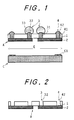
- Fig. 1 is a schematic cross section of one embodiment of the film carrier of the present invention.
- Fig. 2 is a schematic cross section of another embodiment of the film carrier of the present invention.
- Fig. 3 is a schematic view of one embodiment of the conductive part of the film carrier of the present invention, which is constituted by plural kinds of materials.
- Fig. 4 is a schematic cross section of one embodiment of the semiconductor device of the present invention.
- Fig. 5 is a schematic cross section of one embodiment of the method of the present invention for mounting a semiconductor element.
- Fig. 6 is a schematic cross section of another embodiment of the film carrier of the present invention.
- Fig. 7 is a schematic view of one embodiment of the conductive part of the film carrier of the present invention, which is constituted by plural kinds of materials.
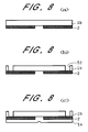
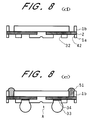
- Fig. 8 is a schematic cross section of one embodiment of the fabrication of the film carrier of the present invention.
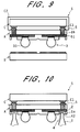
- Fig. 9 is a schematic cross section of another embodiment of the semiconductor device of the present invention.
- Fig. 10 is a schematic cross section of another embodiment of the method of the present invention for mounting a semiconductor element.
- Fig. 1 is a schematic cross section of one embodiment of the film carrier of the present invention.
- A is a film carrier having a conductive circuit 2 laminated on an insulating layer 1.
- Said laminate has a conductive part 3 (conductive path 31) for connecting an external substrate (not shown), and an energy introduction part 4 (conductive path 41) for introducing an energy for connecting a semiconductor element C.
- the material of the insulating layer is subject to no particular limitation as long as it can stably support a conductive circuit, conductive path and the like, and substantially has electrical insulating property.
- Specific examples include various thermosetting resins and thermoplastic resins such as polyester resin, epoxy resin, urethane resin, polystyrene resin, polyamide resin, polyimide resin, acrylonitrile-butadiene-styrene copolymer resin (ABS resin), polycarbonate resin, silicone resin and fluororesin, with preference given to polyimide resin in view of the superior heat resistance, dimensional stability on heating and mechanical strength.
- the thickness of the insulating layer is not particularly limited, it is about 2-500 ⁇ m, preferably about 5-150 ⁇ m, to achieve sufficient mechanical strength and flexibility.
- the material of the conductive circuit is subject to no particular limitation as long as it has conductivity, and is exemplified by various metals (e.g., gold, silver, copper, nickel and cobalt) and various alloys containing them as main components.
- various metals e.g., gold, silver, copper, nickel and cobalt
- various alloys containing them as main components.
- the thickness of the conductive circuit is not particularly limited, it is generally about 1-200 ⁇ m, preferably about 5-80 ⁇ m.
- the laminate of an insulating layer and a conductive circuit can be obtained by, for example, forming a conductive layer on an insulating layer and processing the conductive layer to form a desired circuit pattern (subtractive method).
- a conductive layer is formed on an insulating layer by, for example, coating the insulating layer with a conductive paint containing a metal powder of the above-mentioned various metals or alloys or conductive particles such as carbon black, and a binder such as polyester, or a conductive membrane of the above-mentioned metals is formed on an insulating layer by sputtering, CVD, vacuum evaporation deposition and the like and the membrane is grown to the desired thickness by plating and the like.
- a foil of the above-mentioned metals and form an insulating layer on the foil by applying the above-mentioned various resins or a precursor solution thereof, followed by removal of the solvent, or to adhere a film of the above-mentioned various resins.
- the laminate of an insulating layer and a conductive circuit can be also manufactured by directly processing a conductive material into a circuit pattern without forming a conductive layer (e.g., additive method and semi-additive method).
- the above-mentioned conductive circuit is preferably coated with a metal having high connection reliability, such as gold, to ensure connection to the electrode of a semiconductor element.
- a layer of a barrier metal such as nickel is desirably interposed between said metal coating and the conductive circuit, depending on the kind of the metals used.
- the method for forming the aforementioned metal coating and barrier metal layer includes, for example, plating method such as electrolytic plating and electroless plating, sputtering, ion plating and vacuum evaporation deposition.
- the energy introduction part need only accept the energy for connection from outside and transmit same to the desired contact parts in the conductive circuit to connect the electrode of the semiconductor element.
- the energy introduction part 4 has a conductive path 41.
- the material for said conductive parts 3 and 4 is subject to no particular limitation as long as it has conductivity, and may be known metallic materials, such as gold, silver, copper, platinum, zinc, tin, nickel, cobalt, indium, rhodium, chromium, tungsten and ruthenium, and various alloys containing same as components (e.g., solder, nickel-tin alloy and gold-cobalt alloy).
- a conductive paste containing dispersed conductive particles such as metallic powder and carbon black as mentioned above may be used.
- the conductive parts 3 and 4 are protruded from the surface of the insulating layer 1 in Fig. 1. Accordingly, positioning upon contact with (or connection to) the mating connection parts, such as an energy supply means (not shown) and the electrode of external substrate, is facilitated, and can be performed with certainty.
- the height of the protrusion from the surface of the insulating layer 1 is not particularly limited, but it is suitably about 5-200 ⁇ m to secure contact with (or connection to) the mating connection parts and to improve reliability after connection.
- the shape of the protrusion of the conductive parts 3 and 4 may be like mushroom (umbrella) as shown in Fig. 1, semi-sphere, prism, column, sphere, cone (e.g., circular cone and pyramid) or truncated shape.
- the bottom shape of the protrusion may be triangle, quadrilateral (e.g., square, rectangle, parallelogram and trapezoid), other polygon, circle or ellipse.
- the conductive parts 3 and 4 can be formed by, for example, forming through-holes 32 and 42 in the insulating layer 1, thereby exposing a conductive circuit 2 at the bottom of said through-holes 32 and 42, and filling the through-holes 32 and 42 with a conductive substance.
- a through-hole can be formed by, for example, mechanical processing such as punching, photolithographic processing, plasma processing, chemical etching processing and laser processing, with preference given to laser processing capable of elaborate processing required for fine-pitched products.
- mechanical processing such as punching, photolithographic processing, plasma processing, chemical etching processing and laser processing
- laser processing capable of elaborate processing required for fine-pitched products.
- the use of an ultraviolet laser having an oscillation wavelength in the ultraviolet range is preferable.
- the diameter of the through-hole is about 5-500 ⁇ m.
- the through-hole 42 forming the conductive path 41 preferably has a diameter of about 10-100 ⁇ m
- the through-hole 32 forming the conductive path 31 preferably has a diameter of about 10-300 ⁇ m.
- the method for filling a conductive substance in the above-mentioned through-holes is not limited to a physical filling method comprising injecting a conductive substance into a through-hole with pressure.
- plating method such as electrolytic plating and electroless plating, CVD or chemical filling may be used, which comprises immersing a portion where a through-hole is desired, into a melt metal bath to allow precipitation of a conductive substance.
- an electrolytic plating using a conductive circuit 2 as an electrode facilitates filling of a conductive substance.
- the exposed conductive circuit is desirably plated with a metal which ensures contact with an energy supply means, such as gold, silver, copper and solder.
- the through-hole 32 may be filled with a conductive substance (e.g., solder and conductive paste) immediately before connection to an external substrate.
- a conductive substance e.g., solder and conductive paste
- the conductive part 3 to be connected to an external substrate is formed inside the region E of the laminate of insulating layer 1 and conductive circuit 2, which region being designed to mount semiconductor element C in Fig. 1.
- the size (area) of the semiconductor device can be decreased to, for example, the size of the semiconductor element C, and electrode C1 of the semiconductor element C and a lead of the external substrate can be connected in a short distance, whereby a semiconductor device having superior electric properties can be obtained.
- the conductive part 3 may be formed outside the region E where the semiconductor element C is to be mounted, or at a position bridging both inside and outside said region E. In other words, since the position of the conductive part 3 can be determined optionally, the position of the connection to an external substrate can be unified even when the position of the electrode C1 varies among individual semiconductor elements C, which is desirable for standardizing electronic parts.
- a conductor 33 to be connected to an external substrate is preferably formed on said conductive path 31, as shown in Fig. 1.
- the material of the conductor 33 may be or may not be the same with the material of the conductive path 31. In general, the same material is used, and when the same material is used, the conductor 33 and the conductive path 31 are preferably formed integrally.
- the conductive part 3 and energy introduction part 4 may be made from two or more kinds of materials.
- Fig. 3 is a schematic view of one embodiment of the conductive part 3 (conductive path 311) which is constituted by plural kinds of materials.
- the conductive part 3 in this figure contains an economical metal such as copper for the part 311 in contact with a conductive circuit 2, and a metal highly reliable in connection performance, such as gold, is used for the part 313 to be connected to an external substrate.
- a barrier metal such as nickel which can prevent interaction between the above-mentioned two kinds of metals is used for the intermediate part 312 in between the above-mentioned two parts 311 and 313.
- Fig. 4 is a schematic cross section of one embodiment of the semiconductor device of the present invention.
- electrode C1 of semiconductor element C is connected to conductive circuit 2 of the film carrier A of the present invention, which is the same as the one shown in Fig. 1, to mount the semiconductor element C on said film carrier A.
- the size (area) of the semiconductor device S is about the same as the size (area) of the semiconductor element C.
- Fig. 5 includes schematic cross sections showing one embodiment of the present invention for mounting a semiconductor element.
- electrode C1 of semiconductor element C is brought into contact with the conductive circuit 2 of the film carrier A of the present invention, which is the same as the one shown in Fig. 1, and an energy is applied to said contact part via energy introduction part 4 in the film carrier A, as shown in Fig. 5(b), to connect said conductive circuit 2 to electrode C1, whereby a semiconductor device S which is the same as the one shown in Fig. 4 is obtained, as shown in Fig. 5(c).
- the contact between the conductive circuit 2 and electrode C1 of semiconductor element C is accomplished by bringing the energy supply means T into contact with the energy introduction part 4 (conductive path 41 in Fig. 5), as shown in Fig. 5(b), and supplying the energy for the connection of the conductive circuit 2 to electrode C1 from the energy supply means T.
- the energy for said connection is exemplified by heat, ultrasonic wave, pressure and a combination of these, which is determined as appropriate according to the materials constituting the semiconductor element C and film carrier A.
- an energy supply means T is brought into contact with the exposed part of the conductive circuit 2 at the bottom of through-hole 42 to supply an energy for the connection of the conductive circuit 2 with electrode C1.
- Fig. 6 is a schematic cross section of one embodiment of the film carrier of the present invention, wherein A is a film carrier comprising insulating layers 1a and 1b laminated on the both sides of the conductive circuit 2.
- This laminate contains a conductive part 3 to be connected to an external substrate B and a conductive part 5 to be connected to a semiconductor element C, and the insulating layer 1a is partially removed on the opposite side from the conductive part 5 to expose part of the conductive circuit.
- the conductive circuit is mostly covered with an insulating layer on both sides and is not exposed.
- the insulating layers 1a and 1b have through-holes 32 and 52, respectively, which reach the surface of the conductive circuit.
- a conductive layer 34 is formed for improving connection to the conductive circuit and a ball 33 to be connected to an external substrate, thereby constituting the conductive part 3 to be connected to the external substrate B.
- the insulating layer 1a preferably has a thickness of about 7-20 ⁇ m so that it will not pose problems for the insertion of a jig (hereinafter to be referred to as energy supply jig) used for the application of energy to connect the semiconductor element.
- energy supply jig a jig
- the materials of the insulating layers 1a and 1b are as exemplified above wherein the materials may be the same or different.
- the conductive circuit is basically covered with insulating layers 1a and 1b and is not exposed. Therefore, the pattern of the conductive circuit can be freely designed irrespective of the pattern of the semiconductor element.
- the conductive circuit may be formed in a multi-layer structure of two or more layers. Such construction enables three-dimensional design of the conductive circuit to allow fine-pitched or highly dense mounting.
- the conductive part to be connected to the semiconductor element may be formed from a single kind of material or from two or more kinds of materials.
- Fig. 7 is a schematic view of one embodiment of the conductive part constituted by plural kinds of materials.
- a cheap metal such as copper is used for the part 521 in contact with the conductive circuit 2
- a metal highly reliable in connection performance, such as gold is used for the part 523 to be connected to electrode C1 of semiconductor element C
- a barrier metal such as nickel which can prevent an interaction between the above-mentioned two kinds of metals is used for the intermediate part 522 in between the above-mentioned two parts 521 and 523.
- the conductive part 5 may be formed from four or more kinds of materials.
- the conductive part 5 is protruded from the surface of the insulating layer 1b in Fig. 6. Therefore, positioning for the connection with the electrode C1 of the semiconductor element C is facilitated and the connection is ensured. While the height of the protrusion from the surface of the insulating layer 1b is not particularly limited, in view of an ensured connection to the electrode, it is suitably about 0.1-50 ⁇ m.
- the end portion of the conductive part 5 can be optionally modified in shape according to the layout and shape of the electrode of the semiconductor element.
- the end portion of the conductive part 5 is preferably made to have a mushroom-like shape or cone with a pointing tip.
- the end portion of the conductive part 5 is preferably made to have a planar end surface, such as prism or column.
- the end surface is a plane, as in the latter case, the end portion of the conductive part 5 may be at the even level with the surface of the insulating layer 1b.
- the conductive part 3 has a conductive layer 34 for improving connection to the conductive circuit 2, and a ball conductor 33 to be connected to the external substrate B.
- the material of the conductor layer 34 may be any as long as it has conductivity, and is exemplified by the same kinds of metals exemplified for the conductive part or various alloys containing same as components. Particularly preferred is gold which has high connection reliability.
- the thickness of the conductive layer is not particularly limited, it is suitably about 0.01-10 ⁇ m to improve connection of the ball to the conductive circuit.
- the material of the ball is exemplified by the same kinds of metals exemplified for the conductive part and various alloys containing same as components. Particularly preferred is solder which has superior shape modification performance and connection reliability.
- the size of the ball is not particularly limited and may be determined as appropriate according to, for example, the size of the lead of the external substrate B. Generally, its diameter is suitably about 30-500 ⁇ m.
- the shape of the ball may be other than the shape shown in Fig. 6, such as mushroom and cone, like the end portion of the conductive part 5 mentioned above.
- the ball may be formed on the through-hole 32 when manufacturing the film carrier A, or formed immediately before connecting the film carrier A to the external substrate B.
- the exposed part (4 in Fig. 6) of the conductive circuit, which is defined by the insulating layer 1a, is the part from which an energy for making a connection to the semiconductor element is introduced.
- a through-hole 42 is formed in the insulating layer 1a opposite from the conductive part 5 (conductive path 51) to be connected to the semiconductor element C, and the conductive circuit is exposed at the bottom of the through-hole 42.
- the shape of the through-hole 42 need only correspond to the energy supply jig, and is exemplified by circle, square and polygon, with preference given to circle.
- the area of the exposed part 4 of the conductive circuit (area of the opening of through-hole 42 which forms exposed part 4 in Fig. 6) is 50-200%, preferably 70-150%, more preferably 80-130%, of the area of the conductive part 5 to be connected to the semiconductor element C (area of opening of through-hole 52 which forms conductive path 51 in Fig. 6).
- the area of the exposed part 4 is not more than 200% of the area of the conductive part 5, release of the heat to be the energy to make a connection to a semiconductor element, or dispersion of the ultrasonic oscillation, which phenomena being caused by too large an area of the exposed part 4, occurs less.
- easy recognition of the position of conductive part 5 leads to less occurrence of connection failure.
- absorption of the ultrasonic oscillation by insulating layer 1a due to the contact of the energy supply jig with the insulating layer 1a is less.
- the conductive circuit exposed at the bottom of the through-hole 42 may be plated with gold, platinum, palladium, ruthenium and the like on the surface thereof for the prevention of oxidation.
- the above-mentioned film carrier A can be prepared by, for example, the method shown in Fig. 8.
- the fabrication of the film carrier A is explained in the following in the order of the steps shown in Fig. 8.
- the through-hole 52 may be formed after forming the insulating layer 1a, or through-holes 32 and 42 may be formed after forming the conductive path 51.
- the fabrication steps may be subject to partial modification besides these.
- Fig. 9 is a schematic cross section of one embodiment of the semiconductor device of the present invention.
- electrode C1 of semiconductor element C is connected to the conductive part 5 (conductive path 51) to be connected to the semiconductor element C of the film carrier A of the present invention, which is the same as the one shown in Fig. 1, and the semiconductor element C is mounted on the film carrier A.
- the semiconductor element C mounted on the film carrier A is covered with an insulating resin layer C2, and this insulating resin layer contacts the insulating layer 1b of the film carrier A.
- the size (area) of the semiconductor device S is about the same as the size (area) of the semiconductor element C.
- the semiconductor element C and the external substrate B are conducted in the direction of the thickness of the film carrier A.
- Fig. 10 is a schematic cross section of one embodiment of the method for mounting a semiconductor element C on the film carrier A.
- electrode C1 of semiconductor element C is connected to the conductive part 5 of the film carrier A of the present invention, which is the same as the one shown in Fig. 1, an energy supply jig T is inserted into the through-hole 42, the energy supply jig T is placed in contact with the exposed part 4 of the conductive circuit, and the energy for connecting semiconductor element is supplied from said energy supply jig T to connect the conductive part 5 to the electrode C1, whereby a semiconductor device S, which is the same as the one shown in Fig. 4, is obtained.
- a 25 ⁇ m thick polyimide resin layer was formed on a 18 ⁇ m thick copper foil, and the copper foil was processed to give a circuit pattern by etching, whereby a laminate of an insulating layer and a conductive circuit was obtained.
- This conductive circuit was plated with gold (thickness 1 ⁇ m) by electrolytic plating. Then, the conductive part in the insulating layer, which was to be connected to the external substrate, and the part where an energy introduction part was to be formed were subjected to a laser processing to give through-holes having a diameter of 60 ⁇ m.
- Said through-holes were filled with copper by electrolytic plating using the conductive circuit as an electrode, and subjected to gold plating (thickness 1 ⁇ m) to prevent oxidation of the copper, whereby to give a conductive path to be connected to an external substrate and an energy introduction part to connect a semiconductor element.
- These conductive path and energy introduction part protruded 10 ⁇ m from the insulator surface in a mushroom shape.
- a ball-shaped portion having a diameter of about 120 ⁇ m was formed, using a solder, on the upper end of the conductive path to be connected to the external substrate, whereby a film carrier which was the same as the one shown in Fig. 1 was obtained.
- the electrode of the semiconductor element was brought into contact with the conductive circuit of the above-mentioned film carrier, and a bonding tool was placed in the energy introduction part of said film carrier to supply ultrasonic wave energy. While supplying the energy, the conductive circuit and the electrode of the semiconductor element were adhered by compression to give a semiconductor device which was the same as the one shown in Fig. 4.
- Example 2 In the same manner as in Example 1 except that copper was not filled in the through-holes, and the conductive path to be connected to the external substrate and the energy introduction part were not formed to have a protrusion shape, a film carrier was prepared.
- the electrode of a semiconductor element was brought into contact with the conductive circuit of the above-mentioned film carrier, and a bonding tool was placed in the energy introduction part of said film carrier. While supplying heat and ultrasonic wave energy to the conductive circuit exposed at the bottom of the through-hole, the conductive circuit and the electrode of the semiconductor element were adhered by compression to give a semiconductor device.
- the semiconductor devices obtained in Examples 1 and 2 had approximately the same size with the semiconductor element. In these semiconductor devices, the continuity of the conductive circuit of the film carrier and the electrode of the semiconductor element was tested to find it in good condition.
- the electrode C1 of the semiconductor element C was brought into contact with the conductive part 5 of the above-mentioned film carrier A, and an energy supply jig T was inserted in the through-hole 42 in the second insulating layer 1a to place the energy supply jig T in the exposed part 4 of the conductive circuit.
- Ultrasonic wave oscillation was applied from the energy supply jig T to connect said conductive part 5 to the electrode C1 of the semiconductor element C, whereby a semiconductor device S which was the same as the one shown in Fig. 9 was obtained.
- the present invention has enabled provision of fine-pitched or highly dense wiring of a semiconductor element, and assures easy and dependable electric connection of a film carrier to a semiconductor element.
- the construction of the present invention wherein an energy for connection is supplied from the energy introduction part to make a connection of a film carrier to a semiconductor element is advantageous in that attenuation of the energy for connection due to an insulating layer occurs less, since the energy for connection can be directly introduced into conductive circuit, thus enabling efficient utilization of the energy, which in turn permits easy and efficient mounting of a semiconductor element.
Landscapes
- Wire Bonding (AREA)
Applications Claiming Priority (2)
| Application Number | Priority Date | Filing Date | Title |
|---|---|---|---|
| JP7165792A JP3015712B2 (ja) | 1995-06-30 | 1995-06-30 | フィルムキャリアおよびそれを用いてなる半導体装置 |
| JP165792/95 | 1995-06-30 |
Publications (3)
| Publication Number | Publication Date |
|---|---|
| EP0751565A2 true EP0751565A2 (fr) | 1997-01-02 |
| EP0751565A3 EP0751565A3 (fr) | 1998-09-30 |
| EP0751565B1 EP0751565B1 (fr) | 2008-08-13 |
Family
ID=15819087
Family Applications (1)
| Application Number | Title | Priority Date | Filing Date |
|---|---|---|---|
| EP96110472A Expired - Lifetime EP0751565B1 (fr) | 1995-06-30 | 1996-06-28 | Bande de support pour semi-conducteurs |
Country Status (5)
| Country | Link |
|---|---|
| US (1) | US5821626A (fr) |
| EP (1) | EP0751565B1 (fr) |
| JP (1) | JP3015712B2 (fr) |
| KR (1) | KR100391022B1 (fr) |
| DE (1) | DE69637635D1 (fr) |
Cited By (7)
| Publication number | Priority date | Publication date | Assignee | Title |
|---|---|---|---|---|
| EP0843357A1 (fr) * | 1996-11-19 | 1998-05-20 | Texas Instruments Inc. | Procédé de fabrication d'un boítier semi-conducteur à réseau de contacts |
| WO2000013232A1 (fr) * | 1998-08-27 | 2000-03-09 | Minnesota Mining And Manufacturing Company | Contact de type bosse pour trou traversant |
| EP1035579A3 (fr) * | 1999-03-05 | 2001-03-07 | Altera Corporation | Methode de fabrication et structure d'un boítier pour des semi-conducteurs |
| WO2001065602A1 (fr) | 2000-02-28 | 2001-09-07 | Hitachi Chemical Co., Ltd. | Plaquette de connexions, dispositif semi-conducteur et procede de fabrication de la plaquette de connexions |
| EP0973197A3 (fr) * | 1998-07-16 | 2002-08-21 | Nitto Denko Corporation | Structure d'empaquetage à l'échelle de plaquette et panneau de circuit utilisé là-dedans |
| EP0999588A3 (fr) * | 1998-11-06 | 2003-01-08 | Sony Corporation | Dispositif semi-conducteur et procédé de sa fabrication |
| US7446399B1 (en) | 2004-08-04 | 2008-11-04 | Altera Corporation | Pad structures to improve board-level reliability of solder-on-pad BGA structures |
Families Citing this family (30)
| Publication number | Priority date | Publication date | Assignee | Title |
|---|---|---|---|---|
| JP3554650B2 (ja) * | 1997-03-21 | 2004-08-18 | ソニーケミカル株式会社 | 回路基板 |
| JPH11163022A (ja) * | 1997-11-28 | 1999-06-18 | Sony Corp | 半導体装置、その製造方法及び電子機器 |
| JP2000106482A (ja) * | 1998-07-29 | 2000-04-11 | Sony Chem Corp | フレキシブル基板製造方法 |
| JP3524425B2 (ja) * | 1999-04-01 | 2004-05-10 | キヤノン株式会社 | マイクロ構造体アレイ用金型又は金型マスターの作製方法、該金型又は金型マスターを用いて作製されるマイクロ構造体アレイの作製方法 |
| JP3524424B2 (ja) * | 1999-04-01 | 2004-05-10 | キヤノン株式会社 | マイクロ構造体アレイ用金型又は金型マスター、及びその作製方法 |
| JP4222690B2 (ja) * | 1999-07-12 | 2009-02-12 | ソニーケミカル&インフォメーションデバイス株式会社 | フレキシブル配線基板素片及び配線シート |
| JP3213292B2 (ja) * | 1999-07-12 | 2001-10-02 | ソニーケミカル株式会社 | 多層基板、及びモジュール |
| JP2001044589A (ja) | 1999-07-30 | 2001-02-16 | Nitto Denko Corp | 回路基板 |
| CN1282981C (zh) * | 1999-10-19 | 2006-11-01 | 松下电器产业株式会社 | 金属电极的制作方法 |
| US6448106B1 (en) * | 1999-11-09 | 2002-09-10 | Fujitsu Limited | Modules with pins and methods for making modules with pins |
| JP3813402B2 (ja) * | 2000-01-31 | 2006-08-23 | 新光電気工業株式会社 | 半導体装置の製造方法 |
| US20040195516A1 (en) * | 2001-02-23 | 2004-10-07 | Brian Matthews | Indium features on multi-contact chips |
| JP2002111185A (ja) * | 2000-10-03 | 2002-04-12 | Sony Chem Corp | バンプ付き配線回路基板及びその製造方法 |
| US6818545B2 (en) * | 2001-03-05 | 2004-11-16 | Megic Corporation | Low fabrication cost, fine pitch and high reliability solder bump |
| JP3812392B2 (ja) * | 2001-10-01 | 2006-08-23 | 日本ビクター株式会社 | プリント配線基板構造及びその製造方法 |
| US7202556B2 (en) * | 2001-12-20 | 2007-04-10 | Micron Technology, Inc. | Semiconductor package having substrate with multi-layer metal bumps |
| SG121707A1 (en) * | 2002-03-04 | 2006-05-26 | Micron Technology Inc | Method and apparatus for flip-chip packaging providing testing capability |
| JP4548571B2 (ja) * | 2002-10-08 | 2010-09-22 | 日本特殊陶業株式会社 | 積層コンデンサの製造方法 |
| JP3707481B2 (ja) * | 2002-10-15 | 2005-10-19 | セイコーエプソン株式会社 | 半導体装置の製造方法 |
| JP3794403B2 (ja) * | 2003-10-09 | 2006-07-05 | セイコーエプソン株式会社 | 半導体装置 |
| JP4119866B2 (ja) * | 2004-05-12 | 2008-07-16 | 富士通株式会社 | 半導体装置 |
| KR100736636B1 (ko) * | 2006-06-16 | 2007-07-06 | 삼성전기주식회사 | 전자소자 패키지용 인쇄회로기판 및 그 제조방법 |
| JP5512082B2 (ja) | 2007-12-17 | 2014-06-04 | 株式会社東芝 | 半導体装置の製造方法及び半導体装置 |
| JP4636090B2 (ja) * | 2008-01-31 | 2011-02-23 | カシオ計算機株式会社 | 半導体装置およびその製造方法 |
| JP4840373B2 (ja) * | 2008-01-31 | 2011-12-21 | カシオ計算機株式会社 | 半導体装置およびその製造方法 |
| CN203242609U (zh) * | 2010-06-02 | 2013-10-16 | 株式会社村田制作所 | Esd保护装置 |
| US20150279824A1 (en) * | 2014-03-28 | 2015-10-01 | Vijay K. Nair | Electronic package and method of forming an electronic package |
| TWI569368B (zh) * | 2015-03-06 | 2017-02-01 | 恆勁科技股份有限公司 | 封裝基板、包含該封裝基板的封裝結構及其製作方法 |
| JP6712050B2 (ja) * | 2016-06-21 | 2020-06-17 | 富士通株式会社 | 樹脂基板及びその製造方法、並びに回路基板及びその製造方法 |
| KR102831521B1 (ko) * | 2023-01-10 | 2025-07-09 | 엘지전자 주식회사 | 플렉서블 디스플레이 디바이스 |
Family Cites Families (8)
| Publication number | Priority date | Publication date | Assignee | Title |
|---|---|---|---|---|
| JPS634638A (ja) * | 1986-06-24 | 1988-01-09 | Nec Corp | フイルムキヤリヤ−テ−プ |
| DE68929282T2 (de) * | 1988-11-09 | 2001-06-07 | Nitto Denko Corp., Ibaraki | Leitersubstrat, Filmträger, Halbleiteranordnung mit dem Filmträger und Montagestruktur mit der Halbleiteranordnung |
| JPH0429338A (ja) * | 1990-05-24 | 1992-01-31 | Nippon Mektron Ltd | Icの搭載用回路基板及びその搭載方法 |
| DE69118308T2 (de) * | 1990-10-24 | 1996-08-08 | Nippon Electric Co | Verfahren zur Herstellung einer elektrischen Verbindung für eine integrierte Schaltung |
| JPH0563029A (ja) * | 1991-09-02 | 1993-03-12 | Fujitsu Ltd | 半導体素子 |
| JPH05326623A (ja) * | 1992-05-25 | 1993-12-10 | Matsushita Electric Works Ltd | Tab用フィルムキャリアの接合方法及びその装置 |
| JP3088877B2 (ja) * | 1992-06-25 | 2000-09-18 | 日東電工株式会社 | フィルムキャリアの製造方法および半導体装置 |
| JP2867209B2 (ja) * | 1993-08-27 | 1999-03-08 | 日東電工株式会社 | フレキシブル回路基板と接触対象物との接続方法およびその構造 |
-
1995
- 1995-06-30 JP JP7165792A patent/JP3015712B2/ja not_active Expired - Fee Related
-
1996
- 1996-06-25 US US08/669,904 patent/US5821626A/en not_active Expired - Lifetime
- 1996-06-28 KR KR1019960024903A patent/KR100391022B1/ko not_active Expired - Fee Related
- 1996-06-28 EP EP96110472A patent/EP0751565B1/fr not_active Expired - Lifetime
- 1996-06-28 DE DE69637635T patent/DE69637635D1/de not_active Expired - Fee Related
Cited By (15)
| Publication number | Priority date | Publication date | Assignee | Title |
|---|---|---|---|---|
| US5989935A (en) * | 1996-11-19 | 1999-11-23 | Texas Instruments Incorporated | Column grid array for semiconductor packaging and method |
| EP0843357A1 (fr) * | 1996-11-19 | 1998-05-20 | Texas Instruments Inc. | Procédé de fabrication d'un boítier semi-conducteur à réseau de contacts |
| EP0973197A3 (fr) * | 1998-07-16 | 2002-08-21 | Nitto Denko Corporation | Structure d'empaquetage à l'échelle de plaquette et panneau de circuit utilisé là-dedans |
| US6864577B2 (en) | 1998-08-27 | 2005-03-08 | 3M Innovative Properties Company | Via plug adapter |
| US6400018B2 (en) | 1998-08-27 | 2002-06-04 | 3M Innovative Properties Company | Via plug adapter |
| WO2000013232A1 (fr) * | 1998-08-27 | 2000-03-09 | Minnesota Mining And Manufacturing Company | Contact de type bosse pour trou traversant |
| EP0999588A3 (fr) * | 1998-11-06 | 2003-01-08 | Sony Corporation | Dispositif semi-conducteur et procédé de sa fabrication |
| EP1035579A3 (fr) * | 1999-03-05 | 2001-03-07 | Altera Corporation | Methode de fabrication et structure d'un boítier pour des semi-conducteurs |
| US6462414B1 (en) | 1999-03-05 | 2002-10-08 | Altera Corporation | Integrated circuit package utilizing a conductive structure for interlocking a conductive ball to a ball pad |
| US6929978B2 (en) | 1999-03-05 | 2005-08-16 | Altera Corporation | Method of fabricating an integrated circuit package utilizing a conductive structure for improving the bond strength between an IC package and a printed circuit board |
| WO2001065602A1 (fr) | 2000-02-28 | 2001-09-07 | Hitachi Chemical Co., Ltd. | Plaquette de connexions, dispositif semi-conducteur et procede de fabrication de la plaquette de connexions |
| EP1271644A4 (fr) * | 2000-02-28 | 2006-02-01 | Hitachi Chemical Co Ltd | Plaquette de connexions, dispositif semi-conducteur et procede de fabrication de la plaquette de connexions |
| US7205645B2 (en) | 2000-02-28 | 2007-04-17 | Hitachi Chemical Co., Ltd. | Wiring board, semiconductor device, and method of manufacturing wiring board |
| US7704799B2 (en) | 2000-02-28 | 2010-04-27 | Hitachi Chemical Co., Ltd. | Method of manufacturing wiring substrate |
| US7446399B1 (en) | 2004-08-04 | 2008-11-04 | Altera Corporation | Pad structures to improve board-level reliability of solder-on-pad BGA structures |
Also Published As
| Publication number | Publication date |
|---|---|
| EP0751565A3 (fr) | 1998-09-30 |
| EP0751565B1 (fr) | 2008-08-13 |
| US5821626A (en) | 1998-10-13 |
| DE69637635D1 (de) | 2008-09-25 |
| KR970003772A (ko) | 1997-01-28 |
| KR100391022B1 (ko) | 2003-09-29 |
| JP3015712B2 (ja) | 2000-03-06 |
| JPH0917829A (ja) | 1997-01-17 |
Similar Documents
| Publication | Publication Date | Title |
|---|---|---|
| US5821626A (en) | Film carrier, semiconductor device using same and method for mounting semiconductor element | |
| JP2899540B2 (ja) | フィルムキャリアおよびこれを用いた半導体装置 | |
| EP0368262B1 (fr) | Substrat à conducteurs, bande de support, dispositif semi-conducteur utilisant la bande de support, et structure de montage comprenant le dispositif semi-conducteur | |
| US6157084A (en) | Film carrier and semiconductor device using same | |
| US6979898B1 (en) | Semiconductor component and a method of fabricating the semiconductor component | |
| US6011310A (en) | Film carrier and semiconductor device using the same | |
| JP3088877B2 (ja) | フィルムキャリアの製造方法および半導体装置 | |
| US4743710A (en) | Coaxial interconnection boards | |
| US6222272B1 (en) | Film carrier and semiconductor device using same | |
| US5691210A (en) | Method for fabrication of probe structure and circuit substrate therefor | |
| JPH06347480A (ja) | プローブ構造 | |
| JPH0727789A (ja) | 回路配線板およびその製造方法 | |
| JP3015709B2 (ja) | フィルムキャリア、それを用いてなる半導体装置ならびに半導体素子の実装方法 | |
| KR100359174B1 (ko) | 필름캐리어및이필름캐리어를이용한반도체장치 | |
| JPH02229445A (ja) | フィルムキャリアおよび半導体装置 | |
| JP3255891B2 (ja) | フィルムキャリア、これらを用いた半導体装置およびフィルムキャリアの製造方法 | |
| JPH0590349A (ja) | 電極付フイルムおよびフイルムキヤリアならびにそれらを用いた半導体装置 | |
| JPH10335388A (ja) | ボールグリッドアレイ | |
| JPH06308158A (ja) | 導通検査装置 | |
| JPH06308196A (ja) | テストヘッド構造 | |
| KR100375643B1 (ko) | 필름캐리어및이를포함하는반도체장치 | |
| JPH0712848A (ja) | プローブ構造およびその製造方法 | |
| JPH08297142A (ja) | プローブ構造 | |
| JP4396863B2 (ja) | 半導体装置、実装基板及びその製造方法、回路基板並びに電子機器 | |
| JPH0627141A (ja) | 複合バンプ付テストヘッドを有するプローブ構造 |
Legal Events
| Date | Code | Title | Description |
|---|---|---|---|
| PUAI | Public reference made under article 153(3) epc to a published international application that has entered the european phase |
Free format text: ORIGINAL CODE: 0009012 |
|
| AK | Designated contracting states |
Kind code of ref document: A2 Designated state(s): DE FR GB NL |
|
| PUAL | Search report despatched |
Free format text: ORIGINAL CODE: 0009013 |
|
| AK | Designated contracting states |
Kind code of ref document: A3 Designated state(s): DE FR GB NL |
|
| 17P | Request for examination filed |
Effective date: 19981113 |
|
| 17Q | First examination report despatched |
Effective date: 20011211 |
|
| 17Q | First examination report despatched |
Effective date: 20011211 |
|
| GRAP | Despatch of communication of intention to grant a patent |
Free format text: ORIGINAL CODE: EPIDOSNIGR1 |
|
| GRAS | Grant fee paid |
Free format text: ORIGINAL CODE: EPIDOSNIGR3 |
|
| GRAA | (expected) grant |
Free format text: ORIGINAL CODE: 0009210 |
|
| AK | Designated contracting states |
Kind code of ref document: B1 Designated state(s): DE FR GB NL |
|
| REG | Reference to a national code |
Ref country code: GB Ref legal event code: FG4D |
|
| RIN2 | Information on inventor provided after grant (corrected) |
Inventor name: SUGIMOTO, MASAKAZU Inventor name: HINO, ATSUSHI Inventor name: MORITA, SHOJI Inventor name: OUCHI, KAZUO |
|
| RAP2 | Party data changed (patent owner data changed or rights of a patent transferred) |
Owner name: NITTO DENKO CORPORATION |
|
| REF | Corresponds to: |
Ref document number: 69637635 Country of ref document: DE Date of ref document: 20080925 Kind code of ref document: P |
|
| NLT2 | Nl: modifications (of names), taken from the european patent patent bulletin |
Owner name: NITTO DENKO CORPORATION Effective date: 20080917 |
|
| PLBE | No opposition filed within time limit |
Free format text: ORIGINAL CODE: 0009261 |
|
| STAA | Information on the status of an ep patent application or granted ep patent |
Free format text: STATUS: NO OPPOSITION FILED WITHIN TIME LIMIT |
|
| 26N | No opposition filed |
Effective date: 20090514 |
|
| PGFP | Annual fee paid to national office [announced via postgrant information from national office to epo] |
Ref country code: NL Payment date: 20090615 Year of fee payment: 14 |
|
| PGFP | Annual fee paid to national office [announced via postgrant information from national office to epo] |
Ref country code: GB Payment date: 20090624 Year of fee payment: 14 Ref country code: DE Payment date: 20090626 Year of fee payment: 14 |
|
| REG | Reference to a national code |
Ref country code: NL Ref legal event code: V1 Effective date: 20110101 |
|
| GBPC | Gb: european patent ceased through non-payment of renewal fee |
Effective date: 20100628 |
|
| REG | Reference to a national code |
Ref country code: FR Ref legal event code: ST Effective date: 20110228 |
|
| PG25 | Lapsed in a contracting state [announced via postgrant information from national office to epo] |
Ref country code: DE Free format text: LAPSE BECAUSE OF NON-PAYMENT OF DUE FEES Effective date: 20110101 |
|
| PG25 | Lapsed in a contracting state [announced via postgrant information from national office to epo] |
Ref country code: FR Free format text: LAPSE BECAUSE OF NON-PAYMENT OF DUE FEES Effective date: 20100630 Ref country code: NL Free format text: LAPSE BECAUSE OF NON-PAYMENT OF DUE FEES Effective date: 20110101 |
|
| PG25 | Lapsed in a contracting state [announced via postgrant information from national office to epo] |
Ref country code: GB Free format text: LAPSE BECAUSE OF NON-PAYMENT OF DUE FEES Effective date: 20100628 |
|
| PGFP | Annual fee paid to national office [announced via postgrant information from national office to epo] |
Ref country code: FR Payment date: 20090611 Year of fee payment: 14 |